Analog Devices AD9786 A Datasheet
16-Bit, 200 MSPS/500 MSPS TxDAC+® with
2×/4×/8× Interpolation and Signal Processing
FEATURES
16-bit resolution, 200 MSPS input data rate
IMD 90 dBc @10 MHz
Noise spectral density (NSD): −164 dBm/Hz @ 10 MHz
WCDMA ACLR = 80 dBc @ 40 MHz IF
DNL = ±0.3 LSB
INL = ±0.6 LSB
Selectable 2×/4×/8× interpolation filters
/2, f
/4, f
Selectable f
DAC
DAC
Single- or dual-channel signal processing
Selectable image rejection Hilbert transform
Flexible calibration engine
Direct IF transmission features
Serial control interface
Versatile clock and data interface
3.3 V-compatible digital interface
On-chip 1.2 V reference
80-lead, thermally enhanced, TQFP_EP package
APPLICATIONS
Base stations: Multicarrier WCDMA, GSM/EDGE, TD-SCDMA,
IS136, TETRA
Instrumentation
RF signal generators, arbitrary waveform generators
HDTV transmitters
Broadband wireless systems
Digital radio links
Satellite systems
/8 modulation modes
DAC
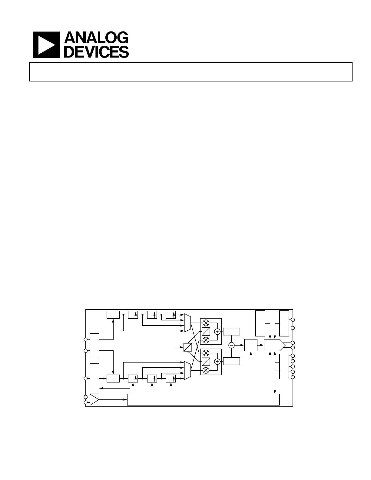
FUNCTIONAL BLOCK DIAGRAM
AD9786
PRODUCT DESCRIPTION
The AD9786 is a 16-bit, high speed, CMOS DAC with
2×/4×/8× interpolation and signal processing features tuned
for communications applications. It offers state-of-the-art
distortion and noise performance. The AD9786 was developed
to meet the demanding performance requirements of
multicarrier and third-generation base stations. The selectable
interpolation filters simplify interfacing to a variety of input
data rates while also taking advantage of oversampling
performance gains. The modulation modes allow convenient
bandwidth placement and selectable sideband suppression.
The flexible clock interface accepts a variety of input types such
as 1 V p-p sine wave, CMOS, and LVPECL in single-ended or
differential mode. Internal dividers generate the required data
rate interface clocks.
The AD9786 provides a differential current output, supporting
single-ended or differential applications; it provides a nominal
full-scale current from 10 mA to 20 mA. The AD9786 is
manufactured on an advanced, low cost, 0.25 µm CMOS process.
LATCH
P1B[15:0]
P2B[15:0]
DATACLK
CLK+
CLK–
Rev. A
Information furnished by Analog Devices is believed to be accurate and reliable.
However, no responsibility is assumed by Analog Devices for its use, nor for any
infringements of patents or other rights of third parties that may result from its use.
Specifications subject to change without notice. No license is granted by implication
or otherwise under any patent or patent rights of Analog Devices. Trademarks and
registered trademarks are the property of their respective owners.
DATA
ASSEMBLER
DATA PORT
SYNCHRONIZER
×1
LATCH
2×2×2×
f
/2
DAC
/4
f
DAC
/8
f
DAC
2×2×2×
CLOCK DISTRIBUTION AND CONTROL
Q
0
90
Q
Figure 1.
FSADJ
0
90
0
90
One Technology Way, P.O. Box 9106, Norwood, MA 02062-9106, U.S.A.
Tel: 781.329.4700
Fax: 781.326.8703 © 2005 Analog Devices, Inc. All rights reserved.
∆t
Re()/Im()
HILBERT
ZERO
STUFF
CALIBRATION
16-BIT DAC
www.analog.com
REFERENCE
SPI
REFIO
CIRCUITS
I
OUTA
I
OUTB
SDIO
SDO
CSB
SCLK
RESET
03152-001

AD9786
TABLE OF CONTENTS
Product Highlights ........................................................................... 3
Specifications..................................................................................... 4
DC Specifications ......................................................................... 4
Dynamic Specifications ............................................................... 5
Digital Specifications ................................................................... 6
Absolute Maximum Ratings............................................................ 7
Thermal Resistance ...................................................................... 7
ESD Caution.................................................................................. 7
Pin Configuration and Function Descriptions............................. 8
Clock .............................................................................................. 8
Analog............................................................................................ 9
Data ................................................................................................ 9
Serial Interface ............................................................................ 10
Definition of Specifications........................................................... 11
Typical Performance Characteristics ........................................... 13
MSB/LSB Transfers .................................................................... 20
Notes on Serial Port Operation ................................................ 20
Mode Control (via Serial Port)..................................................... 21
Digital Filter Specifications........................................................... 25
Digital Interpolation Filter Coefficients.................................. 25
AD9786 Clock/Data Timing..................................................... 26
Real and Complex Signals......................................................... 33
Modulation Modes..................................................................... 34
Power Dissipation....................................................................... 39
Hilbert Transform Implementation......................................... 41
Operating the AD9786 Rev F Evaluation Board........................ 45
Power Supplies............................................................................ 45
PECL Clock Driver .................................................................... 45
Data Inputs.................................................................................. 46
Serial Port.................................................................................... 46
Serial Control Interface.................................................................. 19
General Operation of the Serial Interface............................... 19
Serial Interface Port Pin Descriptions..................................... 19
REVISION HISTORY
2/05—Rev. 0 to Rev. A
Changed DRVDD Supply Range......................................Universal
Changes to DC Specifications......................................................... 4
Changes to Dynamic Specifications............................................... 5
Changes to Digital Specifications................................................... 6
Changes to Absolute Maximum Ratings....................................... 7
Change to Figure 2 ........................................................................... 8
Replaced Figure 13 .........................................................................14
Replaced Figure 14 .........................................................................14
Replaced Figure 16 .........................................................................15
Replaced Figure 21 .........................................................................16
Replaced Figure 22 .........................................................................16
Replaced Figure 26 .........................................................................16
Replaced Figure 27 .........................................................................17
Changes to Table 15........................................................................ 22
Analog Output............................................................................ 46
Outline Dimensions....................................................................... 60
Ordering Guide .......................................................................... 60
Change to Figure 44....................................................................... 26
Replaced Figure 45 ......................................................................... 26
Change to Figure 47....................................................................... 27
Change to Figure 48....................................................................... 27
Change to Figure 51....................................................................... 29
Change to Figure 52....................................................................... 29
Change to Figure 53....................................................................... 30
Change to DATAADJUST Synchronization Section................. 31
Changes to Power Dissipation Section ........................................ 40
Changes to Table 37 ....................................................................... 42
Changes to Data Inputs Section ................................................... 46
Change to Figure 88....................................................................... 49
Replaced Figure 95 ......................................................................... 55
Updated Outline Dimensions....................................................... 60
Changes to Ordering Guide.......................................................... 60
7/04—Revision 0: Initial Version
Rev. A | Page 2 of 60

AD9786
PRODUCT HIGHLIGHTS
1. The AD9786 is a 16-bit, high speed, interpolating
TxDAC+.
2. 2×/4×/8× user-selectable interpolating filter eases data rate
and output signal reconstruction filter requirements.
3. 200 MSPS input data rate.
4. Ultra high speed, 500 MSPS DAC conversion rate.
5. Flexible clock with single-ended or differential input:
CMOS, 1 V p-p sine wave, and LVPECL capability.
6. Complete CMOS DAC function operates from a 3.1 V to
3.5 V single analog (AVDD) supply, 2.5 V digital supply,
and a 3.3 V digital (DRVDD) supply. The DAC full-scale
current can be reduced for lower power operation, and a
sleep mode is provided for low power idle periods.
7. On-chip voltage reference: The AD9786 includes a
1.20 V temperature-compensated band gap voltage
reference.
8. Multichip synchronization: Multiple AD9786 DACs can be
synchronized to a single master AD9786 to ease timing
design requirements and optimize image reject transmit
performance.
Rev. A | Page 3 of 60

AD9786
SPECIFICATIONS
DC SPECIFICATIONS
T
to T
MIN
Table 1.
Parameter Min Typ Max Unit
RESOLUTION 16 Bits
DC Accuracy1
ANALOG OUTPUT
Offset Error ±0.015 ±0.0175 % of FSR
REFERENCE OUTPUT
Reference Voltage 1.15 1.23 1.30 V
Reference Output Current3 1 µA
REFERENCE INPUT
Input Compliance Range 0.1 1.25 V
Reference Input Resistance (External Reference Mode) 10 MΩ
Small Signal Bandwith 200 kHz
TEMPERATURE COEFFICIENTS
Unipolar Offset Drift 0 ppm of FSR/°C
Gain Drift (with Internal Reference) ±4 ppm of FSR/°C
Reference Voltage Drift ±30 ppm/°C
POWER SUPPLY
AVDD1, AVDD2
ACVDD, ADVDD
CLKVDD
DVDD
DRVDD
OPERATING RANGE –40 +85 °C
1
Measured at I
2
Nominal full-scale current, I
3
Use an external amplifier to drive any external load.
4
Measured under the following conditions: f
, AVDD1, AVDD2, DRVDD = 3.3 V, ACVDD, ADVDD, CLKVDD, DVDD = 2.5 V, I
MAX
= 20 mA, unless otherwise noted.
OUTFS
Integral Nonlinearity ±0.6 LSB
Differential Nonlinearity ±0.3 LSB
Gain Error (with Internal Reference) ±1.5 % of FSR
Full-Scale Output Current2 10 20 mA
Output Compliance Range –1.0 +1.0 V
Output Resistance 10 MΩ
Voltage Range 3.1 3.3 3.5 V
Analog Supply Current (I
I
+ I
AVDD1
in Sleep Mode 18 mA
AVDD2
AVDD1
+ I
) 50 mA
AVDD2
Voltage Range 2.35 2.5 2.65 V
Analog Supply Current (I
ACVDD
+ I
) 2.5 mA
ADVDD
Voltage Range 2.35 2.5 2.65 V
Clock Supply Current (I
) 12 mA
CLKVDD
Voltage Range 2.35 2.5 2.65 V
Digital Supply Current (I
) 52.5 mA
DVDD
Voltage Range 3.1 3.3 3.5 V
Digital Supply Current (I
) 5.3 µA
DRVDD
Nominal Power Dissipation4 1.25 W
driving a virtual ground.
OUTA
, is 32× the I
OUTFS
current.
REF
= 125 MSPS, f
DATA
= 500 MSPS, 4× interpolation, f
DAC
/4 modulation, Hilbert off.
DAC
Rev. A | Page 4 of 60

AD9786
DYNAMIC SPECIFICATIONS
T
to T
MIN
, AVDD1, AVDD2, DRVDD = 3.3 V, ACVDD, ADVDD, CLKVDD, DVDD = 2.5 V, I
MAX
coupled output, 50 Ω doubly terminated, unless otherwise noted.
Table 2.
Parameter Min Typ Max Unit
DYNAMIC PERFORMANCE
Minimum DAC Output Update Rate 20 MHz
Maximum DAC Output Update Rate (f
) 500 MSPS
DAC
Output Settling Time (tST) (to 0.025%) ns
Output Propagation Delay1 (tPD) ns
Output Rise Time (10% to 90% of Full Scale)2 ns
Output Fall Time (90% to 10% of Full Scale)2 ns
AC LINEARITY/BASEBAND MODE
Spurious-Free Dynamic Range (SFDR) to Nyquist (f
f
= 100 MSPS; f
DATA
f
= 200 MSPS; f
DATA
f
= 200 MSPS; f
DATA
f
= 200 MSPS; f
DATA
= 5 MHz, 4×, 2× interpolation 93 dBc
OUT
= 10 MHz 85 dBc
OUT
= 25 MHz 78 dBc
OUT
= 50 MHz 78 dBc
OUT
Two-Tone Intermodulation (IMD) to Nyquist (f
f
= 200 MSPS; f
DATA
f
= 200 MSPS; f
DATA
f
= 200 MSPS; f
DATA
f
= 200 MSPS; f
DATA
f
= 200 MSPS; f
DATA
f
= 200 MSPS; f
DATA
= 5 MHz; f
OUT1
= 15 MHz; f
OUT1
= 25 MHz; f
OUT1
= 45 MHz; f
OUT1
= 65 MHz; f
OUT1
= 85 MHz; f
OUT1
= 6 MHz 85 dBc
OUT2
= 16 MHz 85 dBc
OUT2
= 26 MHz 84 dBc
OUT2
= 46 MHz 80 dBc
OUT2
= 66 MHz 78 dBc
OUT2
= 86 MHz 75 dBc
OUT2
= 0 dBFS)
OUT
= f
OUT1
= –6 dBFS)
OUT2
Noise Power Spectral Density (NPSD)
f
= 156 MSPS; f
DATA
f
= 156 MSPS; f
DATA
= 10 MHz; 0 dBFS, 8 tones, separation = 500 kHz −164 dBm/Hz
OUT
= 50 MHz; 0 dBFS, 8 tones, separation = 500 kHz −161 dBm/Hz
OUT
Adjacent Channel Power Ratio (ACLR)
WCDMA ACLR with 3.84 MHz BW, single carrier
IF = 21 MHz, f
IF = 224.76 MHz, f
= 122.88 MSPS, 4× interpolation 80 dB
DATA
= 122.88 MSPS, 4× interpolation, high-pass interpolation filter mode 72 dB
DATA
1
Propagation delay is delay from CLK input to DAC update.
2
Measured doubly terminated into 50 Ω load.
= 20 mA, differential transformer
OUTFS
Rev. A | Page 5 of 60

AD9786
DIGITAL SPECIFICATIONS
T
to T
MIN
Table 3.
Parameter Min Typ Max Unit
DIGITAL INPUTS
Logic 1 Voltage DRVDD – 0.9 DRVDD V
Logic 0 Voltage 0 0.9 V
Logic 1 Current –10 +10 µA
Logic 0 Current –10 +10 µA
Input Capacitance 5 pF
CLOCK INPUTS1
Input Voltage Range 0 2.65 V
Common-Mode Voltage 0.75 1.5 2.25 V
Differential Voltage 0.5 1.5 V
Latch Pulse Width (t
Data Setup Time to DATACLK Out in Master Mode (tS) −0.5 ns
Data Hold Time to DATACLK Out in Master Mode (tH) 2.9 ns
1
See the AD9786 Clock/Data Timing section for setup and hold times in various timing modes.
, AVDD1, AVDD2, DRVDD = 3.3 V, ACVDD, ADVDD, CLKVDD, DVDD = 2.5 V, I
MAX
) 5 ns
LPW
= 20 mA, unless otherwise noted.
OUTFS
Rev. A | Page 6 of 60
AD9786
ABSOLUTE MAXIMUM RATINGS
Table 4.
Parameter With Respect to Min Max Unit
AVDD1, AVDD2,
DRVDD
ACVDD, ADVDD,
CLKGND, DVDD
AGND1, AGND2,
ACGND, ADGND,
CLKGND, DGND
REFIO, FSADJ AGND1 −0.3
I
, I
OUTA
P1B15 to P1B0,
P2B15 to P2B0
DATACLK DGND −0.3
CLK+, CLK−, RESET CLKGND −0.3
CSB, SCLK,
SDIO, SDO
Junction
Temperature
Storage
Temperature
Lead Temperature
(10 sec)
AGND1 −1.0
OUTB
AGND1, AGND2,
ACGND, ADGND,
CLKGND, DGND
AGND1, AGND2,
ACGND, ADGND,
CLKGND, DGND
AGND1, AGND2,
ACGND, ADGND,
CLKGND, DGND
DGND −0.3
DGND −0.3
−65 +125 °C
150 °C
300 °C
−0.3 +3.6 V
−0.3 +2.8 V
−0.3 +0.3 V
AVDD1
+ 0.3
AVDD1
+ 0.3
DRVDD
+ 0.3
DRVDD
+ 0.3
CLKVDD
+ 0.3
DRVDD
+ 0.3
V
V
V
V
V
V
Stresses above those listed under Absolute Maximum Ratings
may cause permanent damage to the device. This is a stress
rating only; functional operation of the device at these or any
other conditions above those indicated in the operational
sections of this specification is not implied. Exposure to
absolute maximum ratings for extended periods may affect
device reliability.
THERMAL RESISTANCE
80-lead thermally enhanced TQFP_EP θJA = 23.5°C/W (with
thermal pad soldered to PCB).
ESD CAUTION
ESD (electrostatic discharge) sensitive device. Electrostatic charges as high as 4000 V readily accumulate
on the human body and test equipment and can discharge without detection. Although this product
features proprietary ESD protection circuitry, permanent damage may occur on devices subjected to
high energy electrostatic discharges. Therefore, proper ESD precautions are recommended to avoid
performance degradation or loss of functionality.
Rev. A | Page 7 of 60
AD9786
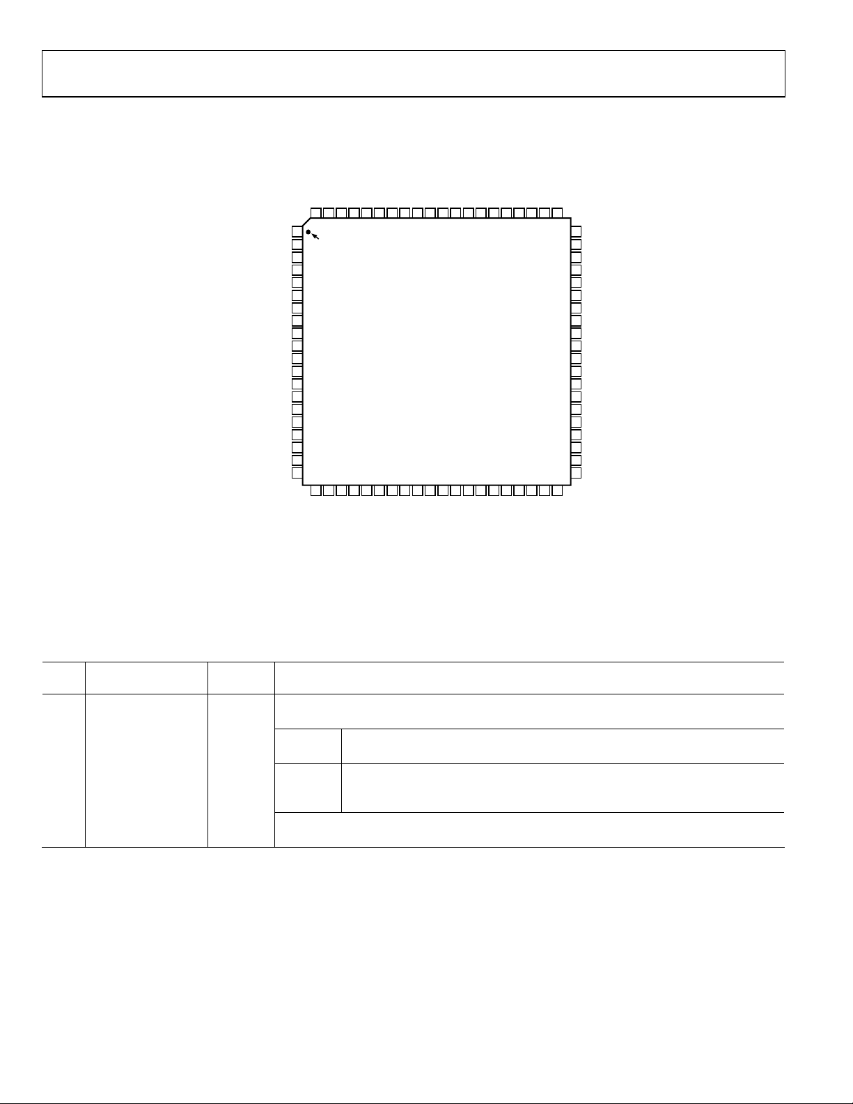
PIN CONFIGURATION AND FUNCTION DESCRIPTIONS
DNC
ADVDD
ADGND
ACVDD
ACGND
AVDD2
AGND2
AVDD1
AGND1
IOUTA
IOUTB
AGND1
DRVDD
DATACLK
AVDD1
IQSEL/P2B15
CLKVDD
DNC
CLKVDD
CLKGND
CLK+
CLK–
CLKGND
DGND
DVDD
P1B15
P1B14
P1B13
P1B12
P1B11
P1B10
DGND
DVDD
P1B9
P1B8
P1B7
DNC = DO NOT CONNECT
80 79 78 77 76 71 70 69 68 67 66 6575 74 73 72 64 63 62 61
1
PIN 1
2
IDENTIFIER
3
4
5
6
7
8
9
10
11
12
13
14
15
16
17
18
19
20
21 22 23 24 25 26 27 28 29 30 31 32 33 34 35 36 37 38 39 40
P1B6
P1B5
P1B4
P1B3
DGND
DVDD
P1B2
AD9786
TOP VIEW
(Not to Scale)
P1B1
P1B0
AGND2
AVDD2
DGND
P2B13
ACGND
ACVDD
DVDD
P2B12
ADGND
ADVDD
P2B11
P2B10
DNC
P2B9
60
59
58
57
56
55
54
53
52
51
50
49
48
47
46
45
44
43
42
41
FSADJ
REFIO
RESET
CSB
SCLK
SDIO
SDO
DGND
DVDD
P2B0
P2B1
P2B2
P2B3
P2B4
P2B5
DGND
DVDD
P2B6
P2B7
P2B8
Figure 2. Pin Configuration
CLOCK
Table 5. Clock Pin Function Descriptions
Pin
No. Mnemonic Direction Description
5, 6 CLK+, CLK– I Differential Clock Input.
2 DNC Do Not Connect.
31 DATACLK I/O
1, 3 CLKVDD Clock Domain 2.5 V.
4, 7 CLKGND Clock Domain 0 V.
DCLKEXT
0x02[3]
0
Mode
Pin configured for input of channel data rate or synchronizer clock. Internal clock
synchronizer can be turned on or off with DCLKCRC (0x02[2]).
1 Pin configured for output of channel data rate or synchronizer clock.
ONEPORTCLOCK/P2B14
03152-002
Rev. A | Page 8 of 60
AD9786
ANALOG
Table 6. Analog Pin Function Descriptions
Pin No. Mnemonic Direction Description
59 REFIO A Reference.
60 FSADJ A Full-Scale Adjust.
70, 71 IOUTB, IOUTA A Differential DAC Output Currents.
61 DNC Do Not Connect.
62, 79 ADVDD Analog Domain Digital Content 2.5 V.
63, 78 ADGND Analog Domain Digital Content 0 V.
64, 77 ACVDD Analog Domain Clock Content 2.5 V.
65, 76 ACGND Analog Domain Clock Content 0 V.
66, 75 AVDD2 Analog Domain Clock Switching 3.3 V.
67, 74 AGND2 Analog Domain Switching 0 V.
68, 73 AVDD1 Analog Domain Quiet 3.3 V.
69, 72 AGND1 Analog Domain Quiet 0 V.
80 DNC Do Not Connect.
DATA
Table 7. Data Pin Function Descriptions
Pin No. Mnemonic Direction Description
10 to 15, 18 to
24, 27 to 29
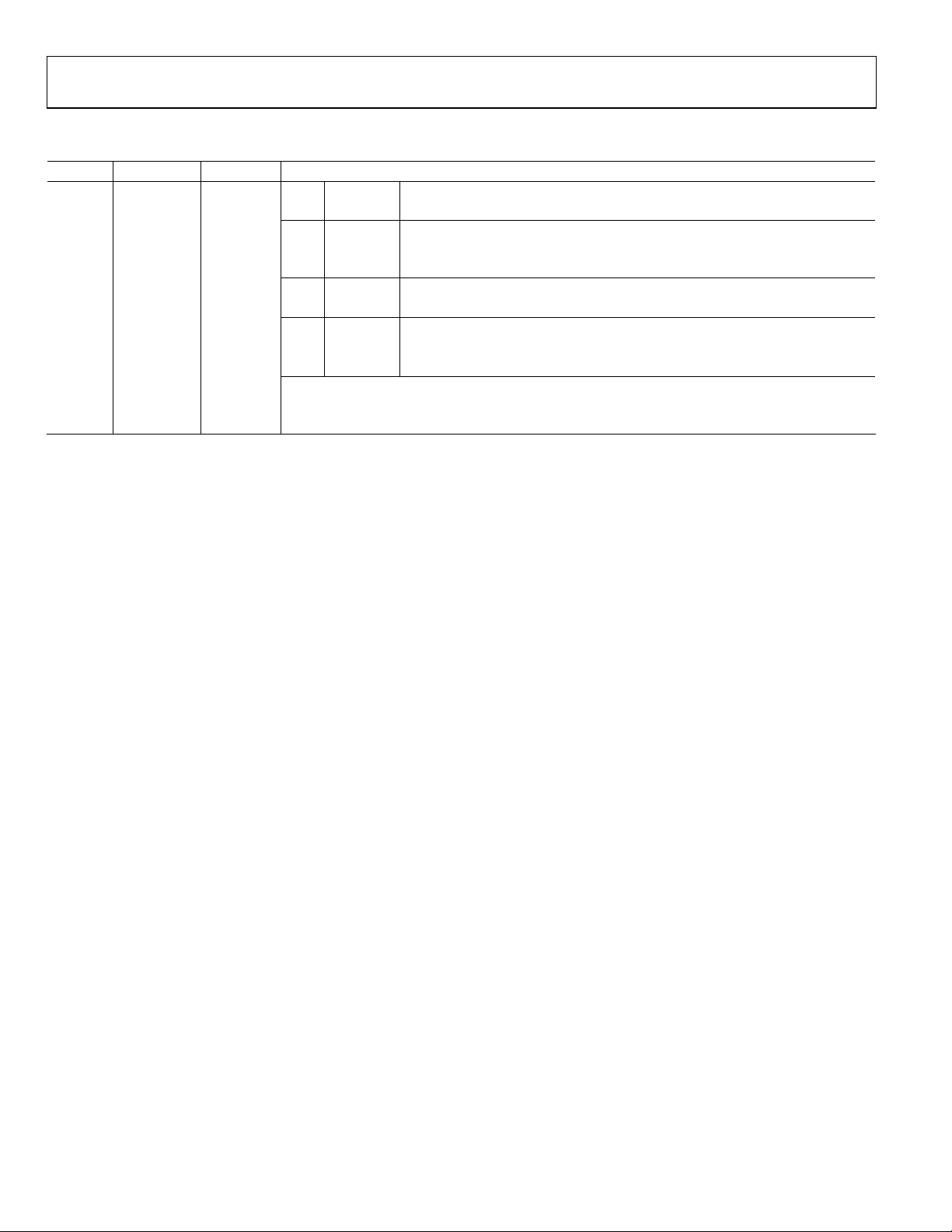
32 IQSEL/P2B15 I
33 ONEPORTCLOCK/P2B14 I/O
34, 37 to 43,
46 to 51
30 DRVDD Digital Output Pin Supply, 3.3 V.
9, 17, 26,
36, 44, 52
8, 16, 25,
35, 45, 53
P1B15 to P1B0 I
P2B13 to P2B0 I Input Data Port 2, Bit 13 to Bit 0.
DVDD Digital Domain, 2.5 V.
DGND Digital Domain, 0 V.
Input Data Port 1.
ONEPORT
0x02[6] Mode
0 Latched data routed for I channel processing.
1
ONEPORT
0x02[6]
0 X X
1 0 0
1 0 1
1 1 0
1 1 1
ONEPORT
0x02[6]
0 Latched data routed for Q channel Bit 14 processing.
1
Latched data demultiplexed by IQSEL and routed for
interleaved I/Q processing.
IQPOL
0x02[1]
Pin configured for output of clock at twice the channel
data route.
IQSEL/
P2B15 Mode (IQPOL = 0)
Latched data routed to Q channel Bit 15
(MSB) processing.
Latched data on Data Port 1 routed to Q
channel processing.
Latched data on Data Port 1 routed to I
channel processing.
Latched data on Data Port 1 routed to I
channel processing.
Latched data on Data Port 1 routed to Q
channel processing.
Rev. A | Page 9 of 60
AD9786
SERIAL INTERFACE
Table 8. Serial Interface Pin Function Descriptions
Pin No. Mnemonic Direction Description
54 SDO O
55 SDIO I/O
56 SCLK I Serial Interface Clock.
57 CSB I Serial Interface Chip Select.
58 RESET I Resets entire chip to default state.
SDIODIR
0x00[7]
CSB
1 X High impedance.
0 0 Serial data output.
0 1 High impedance.
SDIODIR
CSB
0x00[7] Mode
1 X High impedance.
0 0 Serial data output.
0 1 Serial data input/output depending on Bit 7 of the serial instruction byte.
Mode
Rev. A | Page 10 of 60

AD9786
DEFINITION OF SPECIFICATIONS
Linearity Error (Integral Nonlinearity or INL)
Linearity error is defined as the maximum deviation of the
actual analog output from the ideal output, determined by a
straight line drawn from zero to full scale.
Settling Time
The time required for the output to reach and remain within a
specified error band about its final value, measured from the
start of the output transition.
Differential Nonlinearity (DNL)
DNL is the measure of the variation in analog value, normalized to full scale, associated with a 1 LSB change in digital
input code.
Monotonicity
A D/A converter is monotonic if the output either increases or
remains constant as the digital input increases.
Offset Error
The deviation of the output current from the ideal of zero is
called offset error. For I
inputs are all 0s. For I
, 0 mA output is expected when the
OUTA
, 0 mA output is expected when all
OUTB
inputs are set to 1.
Gain Error
The difference between the actual and ideal output span. The
actual span is determined by the output when all inputs are set
to 1s, minus the output when all inputs are set to 0.
Output Compliance Range
The range of allowable voltage at the output of a current-output
DAC. Operation beyond the maximum compliance limits can
cause either output stage saturation or breakdown, resulting in
nonlinear performance.
Glitch Impulse
Asymmetrical switching times in a DAC give rise to undesired
output transients that are quantified by a glitch impulse. It is
specified as the net area of the glitch in pV-sec.
Spurious-Free Dynamic Range
The difference, in dB, between the rms amplitude of the output
signal and the peak spurious signal over the specified bandwidth.
Total Harmonic Distortion
THD is the ratio of the rms sum of the first six harmonic
components to the rms value of the measured fundamental. It is
expressed as a percentage or in decibels.
Signal-to-Noise Ratio (SNR)
SNR is the ratio of the rms value of the measured output signal
to the rms sum of all other spectral components below the
Nyquist frequency, excluding the first six harmonics and dc.
The value for SNR is expressed in decibels.
Interpolation Filter
If the digital inputs to the DAC are sampled at a multiple rate of
(interpolation rate), a digital filter can be constructed that has
f
DATA
a sharp transition band near f
appear around f
(output data rate) can be greatly suppressed.
DAC
/2. Images that would typically
DATA
Temp er at u re D ri ft
Temperature drift is specified as the maximum change from the
ambient (+25°C) value to the value at either T
MIN
or T
MAX
. For
offset and gain drift, the drift is reported in ppm of full-scale
range (FSR) per degree Celsius. For reference drift, the drift is
reported in ppm per degree Celsius.
Power Supply Rejection
The maximum change in the full-scale output as the supplies
are varied from minimum to maximum specified voltages.
Pass Band
Frequency band in which any input applied therein passes
unattenuated to the DAC output.
Stop-Band Rejection
The amount of attenuation of a frequency outside the pass band
applied to the DAC, relative to a full-scale signal applied at the
DAC input within the pass band.
Rev. A | Page 11 of 60

AD9786
Group Delay
Number of input clocks between an impulse applied at the
device input and peak DAC output current. A half-band FIR
filter has constant group delay over its entire frequency range
Impulse Response
Response of the device to an impulse applied to the input.
Adjacent Channel Leakage Ratio (ACLR)
A ratio in dBc between the measured power within a channel
relative to its adjacent channel.
Complex Modulation
The process of passing the real and imaginary components of a
signal through a complex modulator (transfer function = e
coswt + jsinwt) and realizing real and imaginary components
on the modulator output.
jwt
=
Hilbert Transform
A function with unity gain over all frequencies, but with a phase
shift of 90° for negative frequencies, and a phase shift of –90°
for positive frequencies. Although this function can not be
implemented ideally, it can be approximated with a short FIR
filter with enough accuracy to be very useful in single sideband
radio architectures.
Complex Image Rejection
In a traditional two-part upconversion, two images are created
around the second IF frequency. These images are redundant
and have the effect of wasting transmitter power and system
bandwidth. By placing the real part of a second complex
modulator in series with the first complex modulator, either the
upper or lower frequency image near the second IF can be
rejected.
Rev. A | Page 12 of 60
AD9786
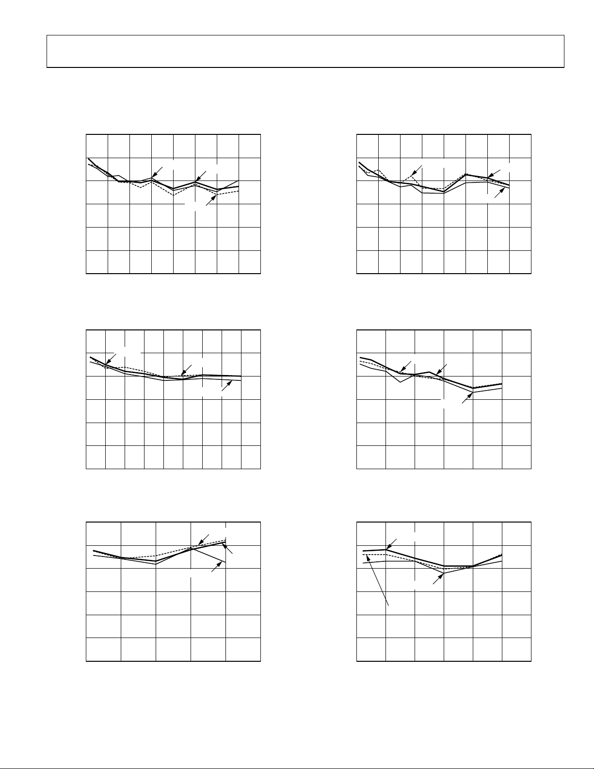
TYPICAL PERFORMANCE CHARACTERISTICS
T
to T
MIN
, AVDD1, AVDD2, DRVDD = 3.3 V, ACVDD, ADVDD, CLKVDD, DVDD = 2.5 V, I
MAX
coupled output, 50 Ω doubly terminated, unless otherwise noted.
120
120
= 20 mA, differential transformer
OUTFS
100
80
60
SFDR (dBc)
40
20
0
Figure 3. SFDR vs. Frequency, F
120
100
80
60
SFDR (dBc)
40
–3dBFS
–6dBFS
0dBFS
FREQUENCY (MHz)
= 200 MSPS, 1× Interpolation
DATA
–6dBFS
0dBFS
–3dBFS
100
80
60
SFDR (dBc)
40
20
800 10203040506070
03152-003
0
Figure 6. SFDR vs. Frequency, F
120
100
80
60
SFDR (dBc)
40
–6dBFS
FREQUENCY (MHz)
= 200 MSPS, 2× Interpolation
DATA
–3dBFS
–6dBFS
0dBFS
0dBFS
–3dBFS
800 10203040506070
03152-006
20
0
Figure 4. SFDR vs. Frequency, F
120
100
80
60
SFDR (dBc)
40
20
0
Figure 5. SFDR vs. Frequency, F
FREQUENCY (MHz)
= 100 MSPS, 4× Interpolation
DATA
0dBFS
FREQUENCY (MHz)
= 50 MSPS, 8× Interpolation
DATA
–6dBFS
–3dBFS
20
450 5 10 15 20 25 30 35 40
03152-004
250 5 10 15 20
03152-005
0
Figure 7. SFDR vs. Frequency, F
120
100
80
60
SFDR (dBc)
40
20
0
–6dBFS
0dBFS
–3dBFS
Figure 8. SFDR vs. Frequency, F
FREQUENCY (MHz)
= 125 MSPS, 4× Interpolation
DATA
FREQUENCY (MHz)
= 62.5 MSPS, 8× Interpolation
DATA
600 1020304050
03152-007
300 5 10 15 20 25
03152-008
Rev. A | Page 13 of 60
AD9786
90
85
80
75
70
65
SFDR (dBc)
60
55
50
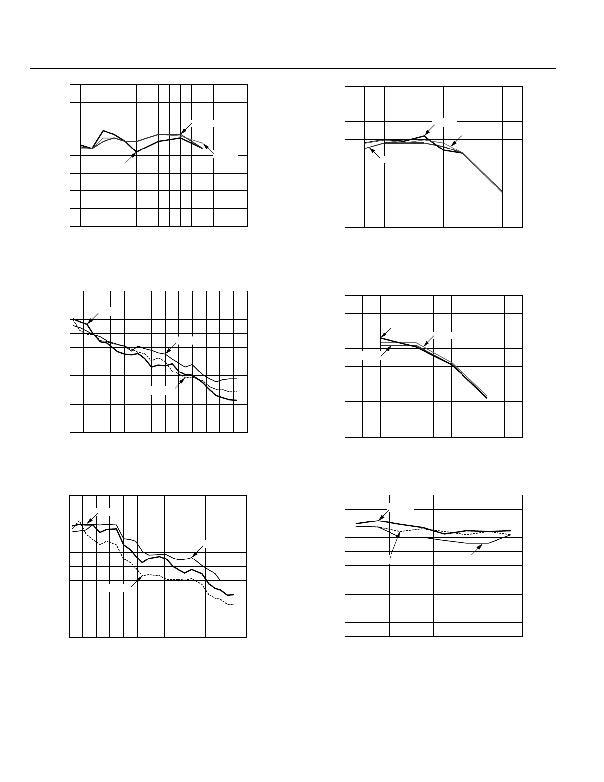
Figure 9. Out-of-Band SFDR, F
0dBFS
–3dBFS
F
(MHz)
OUT
= 200 MSPS, 2× Interpolation
DATA
–6dBFS
90
85
80
75
70
65
60
OUT OF BAND SFDR (dBc)
55
800 102030 607040 50
03152-009
50
010 304020
–6dBFS
ANALOG OUTPUT FREQUENCY (MHz)
Figure 12. Out-of-Band SFDR, F
0dBFS
–3dBFS
= 100 MSPS, 4× Interpolation
DATA
03152-012
100
IMD (dBc)
95
90
85
80
75
70
65
60
55
50
0dBFS
Figure 10. Out-of-Band SFDR, F
100
IMD (dBc)
95
90
85
80
75
70
65
60
55
50
–3dBFS
0dBFS
Figure 11. Out-of-Band SFDR, F
–6dBFS
–3dBFS
F
(MHz)
OUT
= 125 MSPS, 4× Interpolation
DATA
–6dBFS
F
(MHz)
OUT
= 62.5 MSPS, 8× Interpolation
DATA
90
85
80
75
–3dBFS
70
65
60
OUT OF BAND SFDR (dBc)
55
260200 220 2400 20 40 60 120 140 160 18080 100
03152-010
50
Figure 13. Out-of-Band SFDR, F
100
95
90
85
80
75
70
IMD (dBc)
65
60
55
2600 20 40 60 120 140 160 180 200 220 24080 100
03152-011
50
Figure 14. Third-Order IMD vs. Frequency, F
0dBFS
ANALOG OUTPUT FREQUENCY (MHz)
–3dBFS
–6dBFS
–6dBFS
= 50 MSPS, 8× Interpolation
DATA
0dBFS
F
(MHz)
OUT
DATA
250 5 10 15 20
03152-013
800 204060
03152-014
= 160 MSPS, 1× Interpolation
Rev. A | Page 14 of 60
AD9786
100
IMD (dBc)
95
90
85
80
75
70
65
60
55
50
–3dBFS
0dBFS
F
OUT
(MHz)
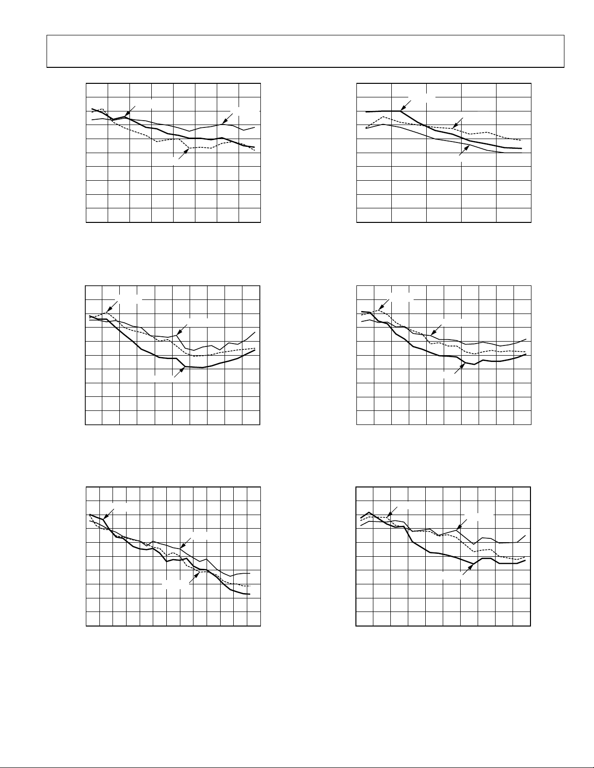
Figure 15. Third-Order IMD vs. Frequency, F
–6dBFS
1600 20 40 60 120 14080 100
= 160 MSPS, 2× Interpolation
DATA
03152-015
100
IMD (dBc)
95
90
85
80
75
70
65
60
55
50
–3dBFS
0dBFS
F
(MHz)
OUT
Figure 18. Third-Order IMD vs. Frequency, F
–6dBFS
10002040 8060
= 200 MSPS,1x Interpolation
DATA
03152-018
100
–3dBFS
0dBFS
F
OUT
(MHz)
IMD (dBc)
95
90
85
80
75
70
65
60
55
50
Figure 16. Third-Order IMD vs. Frequency, F
100
IMD (dBc)
95
90
85
80
75
70
65
60
55
50
0dBFS
F
OUT
–3dBFS
(MHz)
Figure 17. Third-Order IMD vs. Frequency, F
–6dBFS
2000 20 40 60 120 140 160 18080 100
= 200 MSPS, 2× Interpolation
DATA
–6dBFS
260200 220 2400 20 40 60 120 140 160 18080 100
= 125 MSPS, 4× Interpolation
DATA
03152-016
03152-017
100
–3dBFS
F
0dBFS
OUT
–6dBFS
(MHz)
IMD (dBc)
95
90
85
80
75
70
65
60
55
50
Figure 19. Third-Order IMD vs. Frequency, F
100
IMD (dBc)
95
90
85
80
75
70
65
60
55
50
–3dBFS
0dBFS
F
(MHz)
OUT
Figure 20. Third-Order IMD vs. Frequency, F
2000 20 40 60 120 140 160 18080 100
= 100 MSPS, 4× Interpolation
DATA
–6dBFS
2000 20 40 60 120 140 160 18080 100
= 50 MSPS, 8× Interpolation
DATA
03152-019
03152-020
Rev. A | Page 15 of 60
AD9786
100
95
90
85
80
75
70
IMD (dBc)
65
60
55
50
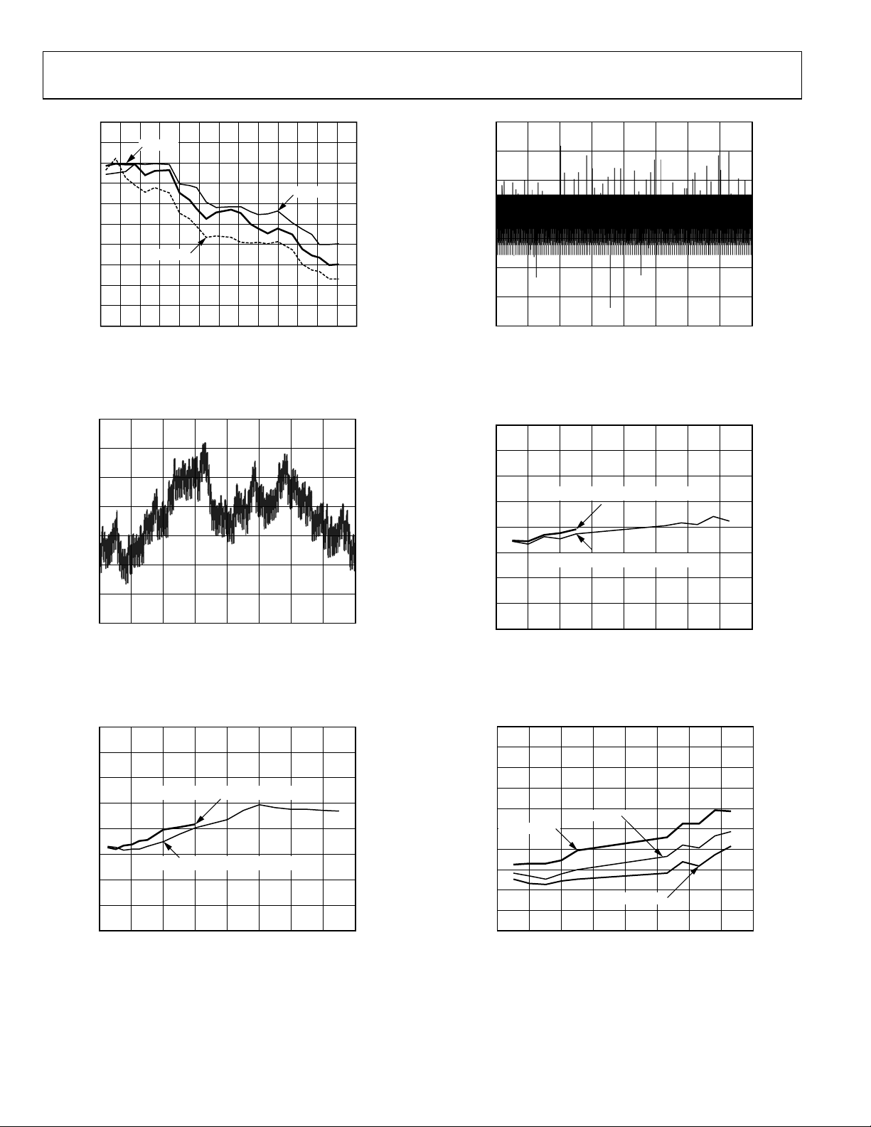
Figure 21. Third-Order IMD vs. Frequency, F
–3dBFS
0dBFS
F
(MHz)
OUT
–6dBFS
2600 204060 12010080 160140 180 200 220 240
= 62.5 MSPS, 8× Interpolation
DATA
03152-021
0.3
0.2
0.1
0
–0.1
DNL (LSBs)
–0.2
–0.3
–0.4
CODE
655360 8192 16384 24576 49152 5734432768 40960
03152-024
Figure 24. Typical DNL
1.25
1.00
0.75
0.50
0.25
INL (LSBs)
–0.25
–0.50
–140
–145
–150
–155
–160
–165
–170
–175
NOISE SPECTRAL DENSITY(dBm/Hz)
–180
0
CODE
Figure 22. Typical INL
F
= 156MSPS, 1× INTERPOLATION
DATA
F
= 156MSPS, 2× INTERPOLATION
DATA
ANALOG OUTPUT FREQUENCY (MHz)
Figure 23. Noise Spectral Density vs. Analog
Input Frequency, F
DATA
= 156 MSPS
–140
–145
–150
F
= 78MSPS, 1× INTERPOLATION
–155
–160
–165
–170
–175
NOISE SPECTRAL DENSITY(dBm/Hz)
655360 8192 16384 24576 49152 5734432768 40960
03152-022
–180
DATA
F
= 78MSPS, 2× INTERPOLATION
DATA
ANALOG OUTPUT FREQUENCY (MHz)
800 102030 607040 50
03152-025
Figure 25. Noise Spectral Density vs. Analog
= –6DBFS
A
IN
= 78 MSPS
DATA
800 10203040506070
03152-026
Input Frequency, F
–150
–152
–154
–156
–158
–160
AIN = 0DBFS
–162
–164
–166
NOISE SPECTRAL DENSITY (dBm/Hz)
–168
1600 20 40 60 120 14080 100
03152-023
–170
A
= –3DBFS
IN
ANALOG OUTPUT FREQUENCY (MHz)
Figure 26. Noise Spectral Density vs. Analog Input Frequency,
= 78 MSPS, 2x Interpolation
F
DATA
Rev. A | Page 16 of 60
AD9786
–
–
–150
–152
–154
A
= –3dBFS
–156
–158
–160
AIN = 0dBFS
IN
–162
= –6dBFS
A
–164
IN
–166
NOISE SPECTRAL DENSITY (dBm/Hz)
–168
–170
ANALOG OUTPUT FREQUENCY (MHz)
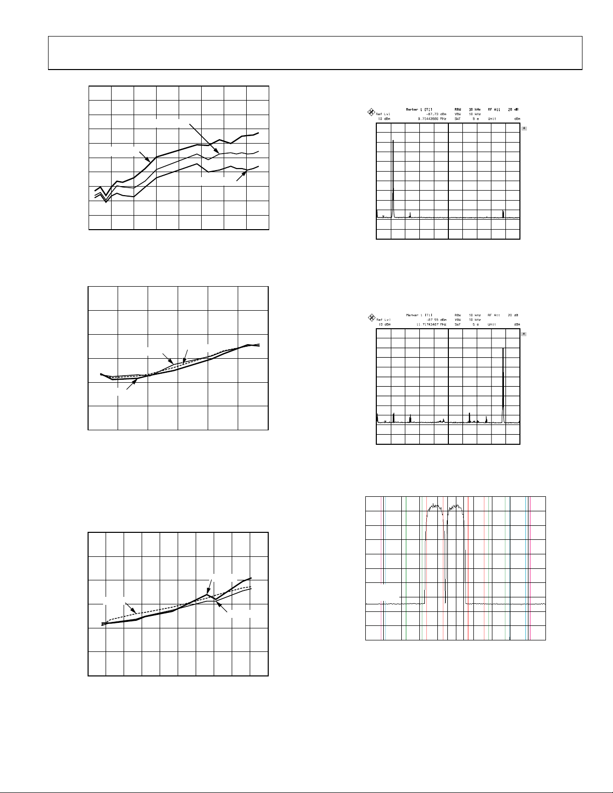
Figure 27. Noise Spectral Density vs. Analog Input Frequency,
= 156 MSPS, 2x Interpolation
F
DATA
–60
–65
1600 20 40 60 80 100 120 140
03152-027
10
0
–10
–20
1AVG
–30
–40
–50
–60
–70
–80
1
–90
100
–110
START 100 kHz STOP 200 MHz19.9 MHz/
Figure 30. Two Tones Around 23 MHz, F
2× Interpolation, Low-Pass Digital Filter Mode
= 200 MSPS,
DATA
1MA
03152-030
–70
–75
ACLR (dBc)
–80
0dBFS
–3dBFS
–6dBFS
–85
–90
F
(MHz)
OUT
Figure 28. ACLR for First Adjacent Band vs. Frequency,
= 61.44 MSPS, 4× Interpolation
F
DATA
–60
–65
–70
0dBFS
–75
ACLR (dBc)
–80
–85
–90
F
(MHz)
OUT
Figure 29. ACLR for First Adjacent Band vs. Frequency,
= 76.8 MSPS, 4× Interpolation
F
DATA
–6dBFS
–3dBFS
10
0
–10
–20
1AVG
–30
–40
–50
–60
–70
–80
1
–90
1500 25 50 75 100 125
03152-028
100
–110
START 100 kHz STOP 200 MHz19.9 MHz/
Figure 31. Two Tones Around 177 MHz, F
= 200 MSPS,
DATA
1MA
03152-031
2× Interpolation, High-Pass Digital Filter Mode
REF –29.82dBm
*AVG
Log
10dB/
AVERAGE
103
PAVG
22
W1 S2
CENTER 51.44MHz
*RES BW 30kHz
RMS RESULTS
CARRIER POWER
2000 20 40 60 80 100 120 140 160 180
03152-029
–17.41dBm/
3.84MHz
*ATTEN 6dB
FREQ OFFSET
5.000MHz
10.000MHz
15.000MHz
20.000MHz
REF BW
3.840MHz
3.840MHz
3.840MHz
3.840MHz
LOWER
dBc
0.15
–74.24
–75.73
–75.67
SWEEP 142.2ms (601 pts)VBW 300kHz
dBm
–17.26
–91.65
–93.14
–93.08
SPAN 43.84MHz
UPPER
dBc
dBm
–74.63
–92.05
–75.67
–93.08
–76.38
–93.79
–75.75
–93.17
03152-032
Figure 32. ACLR for Two WCDMA Carriers @ 51.44 MHz,
= 61.44 MSPS, 4× Interpolation
F
DATA
Rev. A | Page 17 of 60
AD9786
REF –22.76dBm
*AVG
Log
10dB/
AVERAGE
22
PAVG
22
W1 S2
CENTER 20.00MHz
*RES BW 30kHz
RMS RESULTS
CARRIER POWER
–10.38dBm/
3.84 MHz
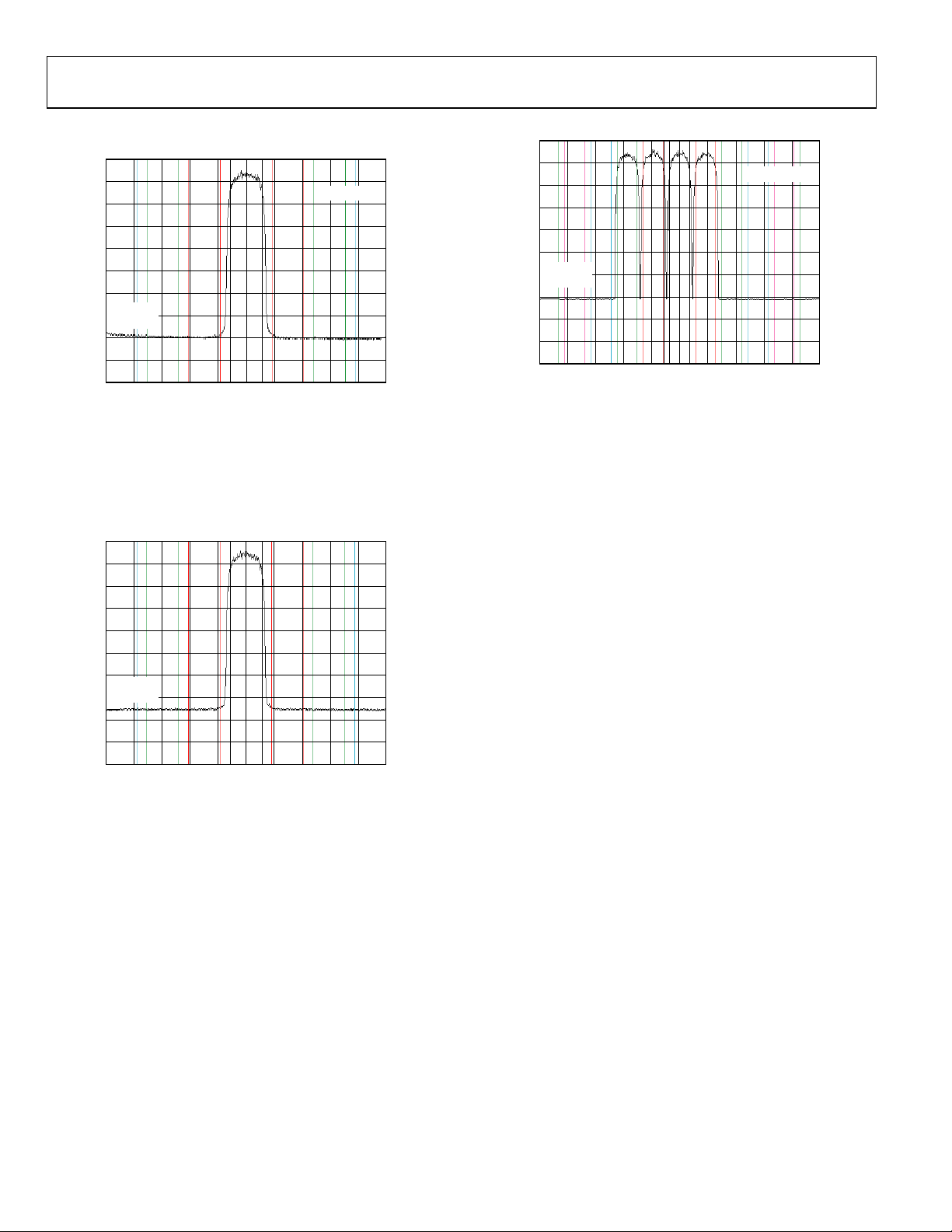
Figure 33. ACLR for Single WCDMA Carrier @ 20 MHz,
*ATTEN 8dB
FREQ OFFSET
5.000MHz
10.000MHz
15.000MHz
F
REF BW
dBc
3.840MHz
–79.00
3.840MHz
–80.78
3.840MHz
–79.71
= 61.44 MSPS, 4× Interpolation
DATA
SWEEP 109.8ms (601 pts)VBW 300kHz
LOWER
dBm
–89.38
–91.16
–90.09
AC-COUPLED
SPAN 33.84MHz
UPPER
dBc
dBm
–79.63
–90.01
–81.77
–92.15
–81.45
–91.83
03152-033
REF –33.3dBm
*AVG
Log
10dB/
AVERAGE
104
PAVG
104
W1 S2
CENTER 46.40MHz
*RES BW 30kHz
RMS RESULTS
CARRIER POWER
–20.32dBm/
3.84MHz
*ATTEN 6dB
FREQ OFFSET
5.000MHz
10.000MHz
15.000MHz
20.000MHz
25.000MHz
REF BW
3.840MHz
3.840MHz
3.840MHz
3.840MHz
3.840MHz
LOWER
dBc
0.22
–0.60
–72.68
–72.74
–73.05
SWEEP 174.6ms (601 pts)VBW 300kHz
dBm
–20.11
–20.92
–93.00
–93.06
–93.37
Figure 35. ACLR for Four WCDMA Carrier Near 50 MHz,
= 61.44 MSPS, 4× Interpolation
F
DATA
AC-COUPLED
SPAN 53.84MHz
UPPER
dBc
dBm
–0.16
–20.48
–72.05
–92.37
–72.85
–93.18
–72.55
–92.88
–72.02
–92.35
03152-035
REF –28.2dBm
*AVG
Log
10dB/
AVERAGE
22
PAVG
22
W1 S2
CENTER 142.88MHz
*RES BW 30kHz
RMS RESULTS
CARRIER POWER
–15.30dBm/
3.84MHz
*ATTEN 6dB
FREQ OFFSET
5.000MHz
10.000MHz
15.000MHz
REF BW
3.840MHz
3.840MHz
3.840MHz
LOWER
dBc
–72.33
–72.41
–72.67
SWEEP 109.8ms (601 pts)VBW 300kHz
dBm
–87.64
–87.71
–87.97
Figure 34. ACLR for Single WCDMA Carrier @ 142.88 MHz,
= 61.44 MSPS, 4× Interpolation
F
DATA
SPAN 33.84MHz
UPPER
dBc
dBm
–72.13
–87.43
–73.02
–88.32
–73.50
–88.88
03152-034
Rev. A | Page 18 of 60
 Loading...