14-Bit, 200 MSPS/500 MSPS TxDAC+® with
Preliminary Technical Data
FEATURES
14-bit resolution, 200 MSPS input data rate
Selectable 2×/4×/8× interpolation filters
/2, f
/4, f
Selectable f
DAC
DAC
Single or dual-channel signal processing
Selectable image rejection Hilbert transform
Flexible calibration engine
Direct IF transmission features
Serial control interface
Versatile clock and data interface
SFDR: 90 dBc @10 MHz
WCDMA ACLR = 80 dBc @ 40 MHz IF
DNL = ±0.75 LSB
INL = ±1.5 LSB
3.3 V compatible digital Interface
On-chip 1.2 V reference
80-lead thermally enhanced TQFP package
APPLICATIONS
Digital quadrature modulation architectures
Multicarrier WCDMA, GSM, TDMA, DCS,
PCS, CDMA Systems
/8 modulation modes
DAC
2×/4×/8× Interpolation and Signal Processing
AD9784
PRODUCT DESCRIPTION
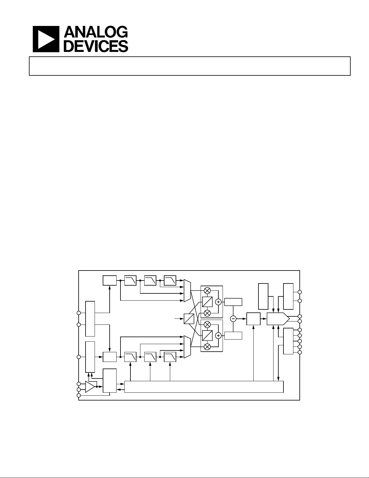
The AD9784 is a 14-bit, high speed, CMOS DAC with 2×/4×/8×
interpolation and signal processing features tuned for communications applications. It offers state of the art distortion and
noise performance. The AD9784 was developed to meet the
demanding performance requirements of multicarrier and third
generation base stations. The selectable interpolation filters
simplify interfacing to a variety of input data rates while also
taking advantage of oversampling performance gains. The
modulation modes allow convenient bandwidth placement and
selectable sideband suppression.
The flexible clock interface accepts a variety of input types such
as 1 V p-p sine wave, CMOS, and LVPECL in single ended or
differential mode. Internal dividers generate the required data
rate interface clocks.
The AD9784 provides a differential current output, supporting
single-ended or differential applications; it provides a nominal
full-scale current from 10 mA to 20 mA. The AD9784 is
manufactured on an advanced low cost 0.25 µm CMOS process.
FUNCTIONAL BLOCK DIAGRAM
LATCH
P1B[15:0]
P2B[15:0]
DATA ASSEMBLER
×1
DATACLK/
PLL_LOCK
CLK+
CLK–
LPF
Rev. PrC
Information furnished by Analog Devices is believed to be accurate and reliable.
However, no responsibility is assumed by Analog Devices for its use, nor for any
infringements of patents or other rights of third parties that may result from its use.
Specifications subject to change without notice. No license is granted by implication
or otherwise under any patent or patent rights of Analog Devices. Trademarks and
registered trademarks are the property of their respective owners.
LATCH
DATA PORT
SYNCHRONIZER
CLOCK
MULTIPLIER
×2 ×4 ×8
2×2×2×
f
/2
DAC
/4
f
DAC
/8
f
DAC
2×2×2×
CLOCK DISTRIBUTION AND CONTROL
I
0
90
Q
Figure 1.
FSADJ
0
90
0
90
One Technology Way, P.O. Box 9106, Norwood, MA 02062-9106, U.S.A.
Tel: 781.329.4700 www.analog.com
Fax: 781.326.8703 © 2004 Analog Devices, Inc. All rights reserved.
∆t
HILBERT
Re()/Im()
ZERO
STUFF
×2/×4/×8/×16
CALIBRATION
16-BIT DAC
×1/×2/×4/×8/×16
CIRCUITS
REFERENCE
SPI
REFIO
I
OUTA
I
OUTB
SDIO
SDO
CSB
SCLK
RESET
03152-PrD-001

AD9784 Preliminary Technical Data
TABLE OF CONTENTS
Product Highlights ........................................................................... 3
Digital Filter Specifications........................................................... 23
AD9784–Specifications.................................................................... 4
DC Specifications ......................................................................... 4
Dynamic Specifications ............................................................... 5
Digital Specifications ................................................................... 6
Pin Configuration and Function Descriptions............................. 7
Clock .............................................................................................. 7
Analog............................................................................................ 8
Data ................................................................................................ 8
Serial Interface ..............................................................................9
Definitions of Specifications ......................................................... 10
Typical Performance Charatceristics ...........................................12
Serial Control Interface.................................................................. 17
General Operation of the Serial Interface ............................... 17
Instruction Byte .......................................................................... 17
Serial Interface Port Pin Descriptions ..................................... 17
Digital Interpolation Filter Coefficients.................................. 23
AD9784 Clock/Data Timing..................................................... 24
Interpolation Modes .................................................................. 27
Real and Complex Signals......................................................... 28
Modulation Modes..................................................................... 29
Power Dissipation ...................................................................... 34
Dual Channel Complex Modulation with Hilbert ................ 35
Hilbert Transform Implementation......................................... 36
Operating the AD9784 Rev E Evaluation Board ........................ 40
Power Supplies............................................................................ 40
PECL Clock Driver .................................................................... 40
Data Inputs.................................................................................. 41
SPI Port........................................................................................ 41
Operating with PLL Disabled ................................................... 41
Operating with PLL Enabled .................................................... 42
MSB/LSB Transfers..................................................................... 18
Notes on Serial Port Operation ................................................ 18
Mode Control (via SPI Port) .........................................................19
REVISION HISTORY
Revision PrC: Preliminary Version
Analog Output............................................................................ 42
Outline Dimensions....................................................................... 52
ESD Caution................................................................................ 52
Rev. PrC | Page 2 of 52

Preliminary Technical Data AD9784
PRODUCT HIGHLIGHTS
1. The AD9784 is a member of a high speed interpolating
TxDAC+ family with 16-/14-/12-bit resolutions.
6. Flexible clock with single-ended or differential input:
CMOS, 1 V p-p sine wave and LVPECL capability.
2. 2×/4×/8× user selectable interpolating filter eases data rate
and output signal reconstruction filter requirements.
3. 200 MSPS input data rate.
4. Ultrahigh speed 500 MSPS DAC conversion rate.
5. Internal PLL/clock divider provides data rate clock for easy
interfacing.
7. Complete CMOS DAC function operates from a 2.7 V to
3.6 V single analog (AVDD) supply and a 2.5 V (DVDD)
digital supply. The DAC full-scale current can be reduced
for lower power operation, and a sleep mode is provided
for low-power idle periods.
8. On-chip voltage reference: The AD9784 includes a 1.20 V
temperature-compensated band gap voltage reference.
Rev. PrC | Page 3 of 52

AD9784 Preliminary Technical Data
AD9784–SPECIFICATIONS
DC SPECIFICATIONS
Table 1. T
otherwise noted
Parameter Min Typ Max Unit
RESOLUTION 14 Bits
DC Accuracy1
Integral Nonlinearity 1.5 LSB
Differential Nonlinearity 0.75 LSB
ANALOG OUTPUT
Offset Error % of FSR
Gain Error (Without Internal Reference) % of FSR
Gain Error (With Internal Reference) % of FSR
Full-Scale Output Current2 10 20 mA
Output Compliance Range –1.0 +1.0 V
Output Resistance TBD kΩ
Output Capacitance 3 pF
REFERENCE OUTPUT
Reference Voltage 1.14 1.20 1.26 V
Reference Output Current3 1 µA
REFERENCE INPUT
Input Compliance Range 0.1 1.25 V
Reference Input Resistance (Ext Reference Mode) 10 MΩ
Small Signal Bandwith 0.5 MHz
TEMPERATURE COEFFICIENTS
Unipolar Offset Drift ppm of FSR/°C
Gain Drift (Without Internal Reference) ppm of FSR/°C
Gain Drift (With Internal Reference) ppm of FSR/°C
Reference Voltage Drift ppm /°C
POWER SUPPLY
AVDD1, AVDD2
Voltage Range 3.1 3.3 3.5 V
Analog Supply Current (I
Analog Supply Current (I
I
AVDD1
ACVDD, ADVDD
Voltage Range 2.35 2.5 2.65 V
Analog Supply Current (I
Analog Supply Current (I
CLKVDD
Voltage Range 2.35 2.5 2.65 V
Clock Supply Current (I
DVDD
Voltage Range 2.35 2.5 2.65 V
Digital Supply Current (I
DRVDD
Voltage Range 2.35 2.5/3.3 3.5 V
Digital Supply Current (I
Nominal Power Dissipation4 1.25 W
OPERATING RANGE –40 +85 °C
1
Measured at IOUTA driving a virtual ground.
2
Nominal full-scale current, I
3
Use an external amplifier to drive any external load.
4
Measured under the following conditions: f
MIN
to T
, AVDD1, AVDD2 = 3.3 V, ACVDD, ADVDD, CLKVDD, DVDD, DRVDD = 2.5 V, I
MAX
) mA
AVDD1
) mA
AVDD2
= 20 mA, unless
OUTFS
in SLEEP Mode mA
) mA
ACVDD
) mA
ADVDD
) mA
CLKVDD
) mA
DVDD
) mA
DRVDD
, is 32× the I
OUTFS
current.
REF
= 125 MSPS, f
DATA
= 500 MSPS, 4× Interpolation, f
DAC
/4 Modulation, Hilbert Off.
DAC
Rev. PrC | Page 4 of 52

Preliminary Technical Data AD9784
DYNAMIC SPECIFICATIONS
Table 2. T
Differential Transformer Coupled Output, 50 Ω Doubly Terminated, unless otherwise noted
Parameter Min Typ Max Unit
DYNAMIC PERFORMANCE
Maximum DAC Output Update Rate (f
Output Settling Time (tST) (to 0.025%) ns
Output Propogation Delay5 (tPD) ns
Output Rise Time (10%–90%)6 ns
Output Fall Time (90%–10%)6 ns
Output Noise (I
AC LINEARITY—BASEBAND MODE
Spurious-Free Dynamic Range (SFDR) to Nyquist (f
f
f
f
f
f
f
Two-Tone Intermodulation (IMD) to Nyquist (f
f
f
f
f
f
f
Total Harmonic Distortion (THD)
f
f
Signal-to-Noise Ratio (SNR)
f
f
Adjacent Channel Power Ratio (ACPR)
WCDMA with MHz BW, MHz Channel Spacing
IF = 16 MHz, f
IF = 32 MHz, f
Four-Tone Intermodulation
MHz, MHz, MHz and MHz at –12 dBFS (f
AC LINEARITY—IF MODE
Four-Tone Intermodulation at IF = MHz
MHz, MHz, MHz and MHz at dBFS dBFS
f
5
Propagation delay is delay from CLK input to DAC update.
6
Measured single-ended into 50 Ω load.
to T
MIN
= 160 MSPS; f
DATA
= MSPS; f
DATA
= MSPS; f
DATA
= MSPS; f
DATA
= MSPS; f
DATA
= MSPS; f
DATA
= 160 MSPS; f
DATA
= MSPS; f
DATA
= MSPS; f
DATA
= MSPS; f
DATA
= MSPS; f
DATA
= MSPS; f
DATA
= MSPS; f
DATA
= MSPS; f
DATA
= MSPS; f
DATA
= MSPS; f
DATA
= MSPS, f
DATA
, AVDD1, AVDD2 = 3.3 V, ACVDD, ADVDD, CLKVDD, DVDD, DRVDD = 2.5 V, I
MAX
) 500 MSPS
DAC
= 20 mA) pA√Hz
OUTFS
= 0 dBFS)
OUT
= 1 MHz 95 dBc
OUT
= MHz dBc
OUT
= MHz dBc
OUT
= MHz dBc
OUT
= MHz dBc
OUT
= MHz
OUT
= f
OUT1
= 25 MHz; f
OUT1
= MHz; f
OUT1
= MHz; f
OUT1
= MHz; f
OUT1
= MHz; f
OUT1
= MHz; f
OUT1
= MHz; 0 dBFS dB
OUT
= MHz; 0 dBFS dB
OUT
= MHz; 0 dBFS dBFS
OUT
= MHz; 0 dBFS dBFS
OUT
= 65.536 MSPS dBc
DATA
= 131.072 MSPS dBc
DATA
= MHz
DAC
OUT2
OUT2
OUT2
OUT2
OUT2
= 31 MHz 80 dBc
OUT2
= MHz dBc
= MHz dBc
= MHz dBc
= MHz dBc
= MHz dBc
= MSPS, Missing Center) dBFS
DATA
= –6 dBFS)
OUT2
OUTFS
= 20 mA,
Rev. PrC | Page 5 of 52

AD9784 Preliminary Technical Data
DIGITAL SPECIFICATIONS
Table 3. T
noted
Parameter Min Typ Max Unit
DIGITAL INPUTS
Logic 1 Voltage DRVDD – 0.9 DRVDD V
Logic 0 Voltage 0 0.9 V
Logic 1 Current –10 +10 µA
Logic 0 Current –10 +10 µA
Input Capacitance 5 pF
LOCK INPUTS
Input Voltage Range 0 2.65 V
Common-Mode Voltage 0.75 1.5 2.25 V
Differential Voltage 0.5 1.5 V
PLL CLOCK ENABLED
Input Setup Time (ts) ns
Input Hold Time (tH) ns
Latch Pulse Width (t
PLL CLOCK DISABLED
Input Setup Time (ts) ns
Input Hold Time (tH) ns
Latch Pulse Width (t
CLK to PLLLOCK Delay (tOD) ns
MIN
to T
, AVDD1, AVDD2 = 3.3 V, ACVDD, ADVDD, CLKVDD, DVDD = 2.5 V, I
MAX
) ns
LPW
) ns
LPW
= 20 mA, unless otherwise
OUTFS
Rev. PrC | Page 6 of 52
Preliminary Technical Data AD9784
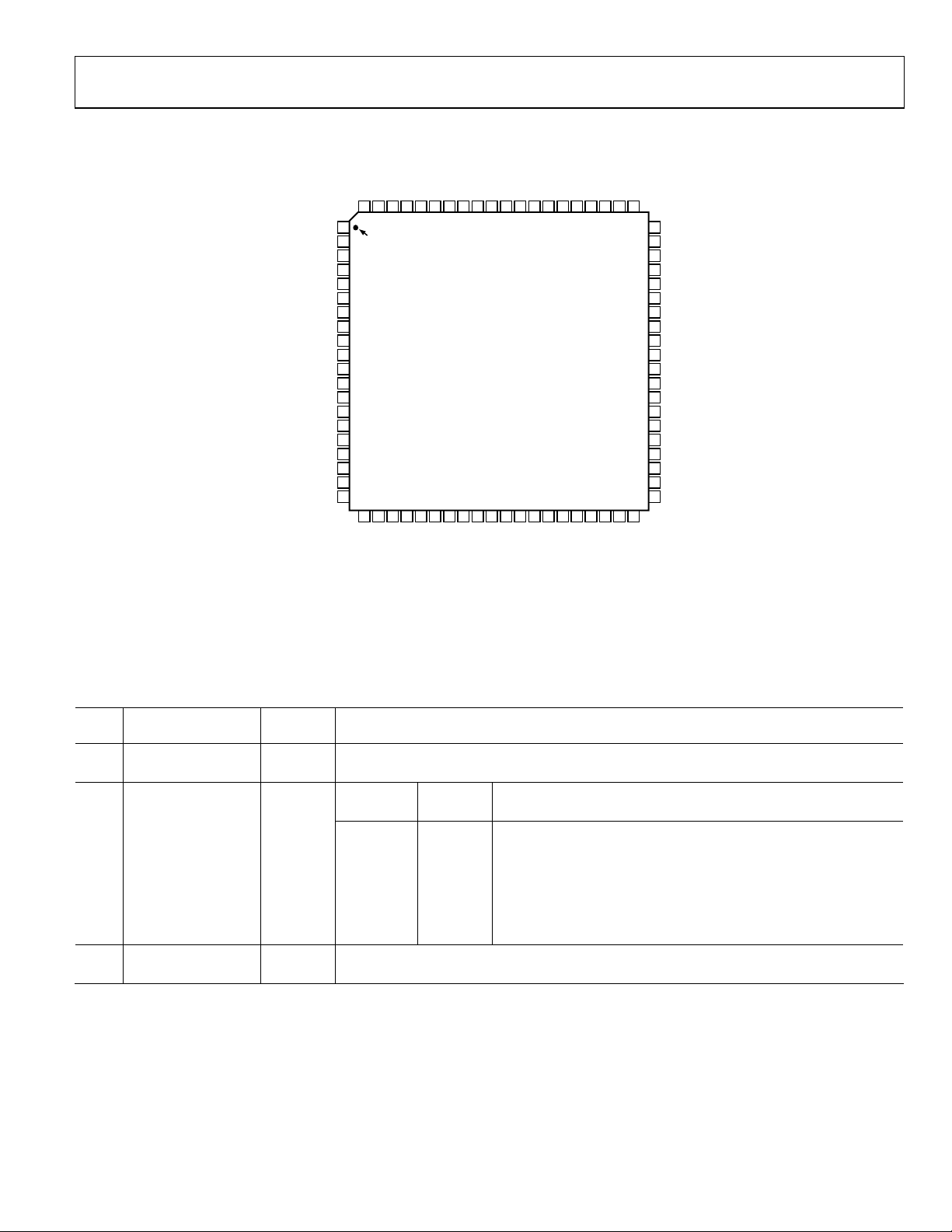
PIN CONFIGURATION AND FUNCTION DESCRIPTIONS
NC
ADVDD
ADGND
ACVDD
ACGND
AVDD2
AGND2
AVDD1
AGND1
IOUTA
IOUTB
AGND1
AVDD1
AGND2
AVDD2
ACGND
ACVDD
ADGND
ADVDD
DNC
FSADJ
60
REFIO
59
RESET
58
CSB
57
SCLK
56
SDIO
55
SDO
54
DGND
53
DVDD
52
P2B0
51
P2B1
50
P2B2
49
P2B3
48
P2B4
47
P2B5
46
DGND
45
DVDD
44
P2B6
43
P2B7
42
P2B8
41
P2B9
P2B11
P2B12
P2B10
CLKVDD
LPF
CLKVDD
CLKGND
CLK+
CLK–
CLKGND
DGND
DVDD
P1B15
P1B14
P1B13
P1B12
P1B11
P1B10
DGND
DVDD
P1B9
P1B8
P1B7
NC = NO CONNECT
80 79 78 77 76 71 70 69 68 67 66 6575 74 73 72 64 63 62 61
1
PIN 1
2
IDENTIFIER
3
4
5
6
7
8
9
10
11
12
13
14
15
16
17
18
19
20
21 22 23 24 25 26 27 28 29 30 31 32 33 34 35 36 37 38 39 40
P1B6
P1B5
P1B4
P1B3
DGND
DVDD
P1B2
AD9784
TOP VIEW
(Not to Scale)
P1B1
P1B0
DRVDD
DGND
P2B13
IQSEL/P2B15
DVDD
Figure 2. Pin Configuration
CLOCK
Table 4. Clock Pin Function Descriptions
Pin
No.
5, 6 CLK+, CLK– I Differential Clock Input.
2 LPF I/O PLL Loop Filter.
31 DATACLK/PLL_LOCK I/O
1, 3 CLKVDD Clock Domain 2.5 V.
4, 7 CLKGND Clock Domain 0 V.
Mnemonic Direction Description
PLOCKEXT
04h[0]
DCLKEXT
02h[3]
0 0
0 1 Pin configured for output of channel data rate or synchronizer clock
1 X Internal Clock PLL Status Output:
DATACLK/PLL_LOCK
ONEPORTCLOCK/P2B14
03151-PrD-001
Mode
Pin configured for input of channel data rate or synchronizer clock.
Internal clock synchronizer may be turned on or off with DCLKCRC
(02h[2]).
0: Internal clock PLL is not locked.
1: Internal clock PLL is locked.
Rev. PrC | Page 7 of 52

AD9784 Preliminary Technical Data
ANALOG
Table 5. Analog Pin Function Descriptions
Pin No. Mnemonic Direction Description
59 REFIO A Reference.
60 FSADJ A Full-Scale Adjust.
70, 71 IOUTB, IOUTA A Differential DAC Output Currents.
61 DNC Do not connect.
62, 79 ADVDD Analog Domain Digital Content 2.5 V.
63, 78 ADGND Analog Domain Digital Content 0 V.
64, 77 ACVDD Analog Domain Clock Content 2.5 V.
65, 76 ACGND Analog Domain Clock Content 0 V.
66, 75 AVDD2 Analog Domain Clock Switching 3.3 V.
67, 74 AGND2 Analog Domain Switching 0 V.
68, 73 AVDD1 Analog Domain Quiet 3.3 V.
69, 72 AGND1 Analog Domain Quiet 0 V.
DATA
Table 6. Data Pin Function Descriptions
Pin No. Mnemonic Direction Description
10–15, 18–24,
27–29
32 IQSEL/P2B15 I
33 ONEPORTCLK/P2B14 I/O
34, 37–43,
46–51
30 DRVDD Digital Output Pin Supply, 2.5 V or 3.3 V.
9, 17, 26,
36, 44, 52
8, 16, 25,
35, 45, 53
P1B15–P1B0 I
P2B13–P2B0 I Input Data Port Two Bits 13–0.
DVDD Digital Domain 2.5 V.
DGND Digital Domain 0 V.
Input Data Port One.
ONEPORT
02h[6] Mode
0 Latched Data Routed for 1 Channel Processing.
1
ONEPORT
02h[6]
0 X X
1 0 0
1 0 1
1 1 0
1 1 1
ONEPORT
02h[6]
0 Latched data routed for Q channel Bit 14 processing.
1 Pin configured for output of clock at twice the channel data route.
Latched Data Demultiplexed by IQSEL and Routed for Interleaved
I/Q Processing.
IQPOL
02h[1]
IQSEL/
P2B15 Mode (IQPOL == 0)
Latched data routed to Q channel bit 15(MSB)
processing.
Latched data on data port one routed to Q
channel processing.
Latched data on data port one routed to I
channel processing.
Latched data on data port one routed to I
channel processing.
Latched data on data port one routed to Q
channel processing.
Rev. PrC | Page 8 of 52

Preliminary Technical Data AD9784
SERIAL INTERFACE
Table 7. Serial Interface Pin Function Descriptions
Pin No. Mnemonic Direction Description
54 SDO O
55 SDIO I/O
56 SCLK I Serial interface clock.
57 CSB I Serial interface chip select.
58 RESET I Resets entire chip to default state.
SDIODIR
00h[7]
CSB
1 X High Impedance.
0 0 Serial Data Output.
0 1 High Impedance.
SDIODIR
CSB
00h[7] Mode
1 X High Impedance.
0 0 Serial Data Output.
0 1 Serial Data Input/Output Depending on Bit 7 of the Serial Instruction Byte.
Mode
Rev. PrC | Page 9 of 52

AD9784 Preliminary Technical Data
DEFINITIONS OF SPECIFICATIONS
Linearity Error (Integral Nonlinearity or INL)
Linearity error is defined as the maximum deviation of the
actual analog output from the ideal output, determined by a
straight line drawn from zero to full scale.
Differential Nonlinearity (or DNL)
DNL is the measure of the variation in analog value, normalized
to full scale, associated with a 1 LSB change in digital input
code.
Monotonicity
A D/A converter is monotonic if the output either increases or
remains constant as the digital input increases.
Offset Error
The deviation of the output current from the ideal of zero is
called offset error. For I
inputs are all 0s. For I
, 0 mA output is expected when the
OUTA
, 0 mA output is expected when all
OUTB
inputs are set to 1s.
Gain Error
The difference between the actual and ideal output span. The
actual span is determined by the output when all inputs are set
to 1s, minus the output when all inputs are set to 0s.
Output Compliance Range
The range of allowable voltage at the output of a current-output
DAC. Operation beyond the maximum compliance limits may
cause either output stage saturation or breakdown, resulting in
nonlinear performance.
Temperature Drift
Temperature drift is specified as the maximum change from the
ambient (+25°C) value to the value at either T
MIN
or T
MAX
. For
offset and gain drift, the drift is reported in ppm of full-scale
range (FSR) per degree C. For reference drift, the drift is
reported in ppm per degree C.
Power Supply Rejection
The maximum change in the full-scale output as the supplies
are varied from minimum to maximum specified voltages.
Glitch Impulse
Asymmetrical switching times in a DAC give rise to undesired
output transients that are quantified by a glitch impulse. It is
specified as the net area of the glitch in pV-s.
Spurious-Free Dynamic Range
The difference, in dB, between the rms amplitude of the output
signal and the peak spurious signal over the specified
bandwidth.
Total Harmonic Distortion
THD is the ratio of the rms sum of the first six harmonic
components to the rms value of the measured fundamental. It is
expressed as a percentage or in decibels (dB).
Signal-to-Noise Ratio (SNR)
S/N is the ratio of the rms value of the measured output signal
to the rms sum of all other spectral components below the
Nyquist frequency, excluding the first six harmonics and dc. The
value for SNR is expressed in decibels.
Interpolation Filter
If the digital inputs to the DAC are sampled at a multiple rate of
(interpolation rate), a digital filter can be constructed
f
DATA
which has a sharp transition band near f
would typically appear around f
(output data rate) can be
DAC
/2. Images which
DATA
greatly suppressed.
Pass-Band
Frequency band in which any input applied therein passes
unattenuated to the DAC output.
Stop-Band Rejection
The amount of attenuation of a frequency outside the passband applied to the DAC, relative to a full-scale signal applied at
the DAC input within the pass-band.
Group Delay
Number of input clocks between an impulse applied at the
device input and peak DAC output current. A half-band FIR
filter has constant group delay over its entire frequency range
Settling Time
The time required for the output to reach and remain within a
specified error band about its final value, measured from the
start of the output transition.
Rev. PrC | Page 10 of 52
Impulse Response
Response of the device to an impulse applied to the input.

Preliminary Technical Data AD9784
Adjacent Channel Power Ratio (or ACPR)
A ratio in dBc between the measured power within a channel
relative to its adjacent channel.
Complex Modulation
The process of passing the real and imaginary components of a
signal through a complex modulator (transfer function = e
coswt + jsinwt) and realizing real and imaginary components
on the modulator output.
jwt
=
Complex Image Rejection
In a traditional two part upconversion, two images are created
around the second IF frequency. These images are redundant
and have the effect of wasting transmitter power and system
bandwidth. By placing the real part of a second complex
modulator in series with the first complex modulator, either the
upper or lower frequency image near the second IF can be
rejected.
Rev. PrC | Page 11 of 52
AD9784 Preliminary Technical Data
TYPICAL PERFORMANCE CHARATCERISTICS
(T
to T
MIN
Coupled Output, 50 Ω Doubly Terminated, unless otherwise noted)
, AVDD1, AVDD2 = 3.3 V, ACVDD, ADVDD, CLKVDD, DVDD, DRVDD = 2.5 V, I
MAX
= 20 mA, Differential Transformer
OUTFS
–000
–000
–000
TBD
ALL CAPS (Initial caps)
–000
–000
–000 –000 –000 –000 –000
Figure 3 Single-Tone Spectrum@ F
–000
–000
–000
ALL CAPS (Initial caps)
= 65 MSPS With F
DATA
TBD
OUT
= F
DATA
/3
–000
–000
–000
TBD
ALL CAPS (Initial caps)
–000
–000
–000 –000 –000 –000 –000
Figure 6. Single-Tone Spectrum @ F
–000
–000
–000
ALL CAPS (Initial caps)
= 78 MSPS with F
DATA
OUT
= F
DATA
/3
TBD
ALL CAPS (Initial caps)
–000
–000
–000 –000 –000 –000 –000
Figure 4. In-Band SFDR vs. F
–000
–000
–000
ALL CAPS (Initial caps)
@ F
OUT
DATA
= 65 MSPS
TBD
ALL CAPS (Initial caps)
–000
–000
–000 –000 –000 –000 –000
Figure 5. Out-of-Band SFDR vs. F
ALL CAPS (Initial caps)
@ F
OUT
= 65 MSPS
DATA
ALL CAPS (Initial caps)
–000
–000
–000 –000 –000 –000 –000
Figure 7. In-Band SFDR Vs. F
–000
–000
–000
ALL CAPS (Initial caps)
@ F
OUT
DATA
= 78 MSPS
TBD
ALL CAPS (Initial caps)
–000
–000
–000 –000 –000 –000 –000
Figure 8. Out-of-Band SFDR vs. F
ALL CAPS (Initial caps)
@ F
OUT
= 78 MSPS
DATA
Rev. PrC | Page 12 of 52
Preliminary Technical Data AD9784
–000
–000
–000
–000
TBD
ALL CAPS (Initial caps)
–000
–000
–000 –000 –000 –000 –000
Figure 9. Single-Tone Spectrum @ F
–000
–000
–000
ALL CAPS (Initial caps)
= 160 MSPS with F
DATA
TBD
ALL CAPS (Initial caps)
–000
OUT
= F
DATA
/3
–000
–000
TBD
ALL CAPS (Initial caps)
–000
–000
–000 –000 –000 –000 –000
Figure 12. Third Order IMD Products vs. F
–000
–000
–000
ALL CAPS (Initial caps)
OUT
@ F
= 65 MSPS
DATA
TBD
ALL CAPS (Initial caps)
–000
–000
–000 –000 –000 –000 –000
Figure 10. In-Band SFDR vs. F
–000
–000
–000
ALL CAPS (Initial caps)
@ F
OUT
DATA
= 160 MSPS
TBD
ALL CAPS (Initial caps)
–000
–000
–000 –000 –000 –000 –000
Figure 11. Out-of-Band SFDR vs. F
ALL CAPS (Initial caps)
@ F
OUT
= 160 MSPS
DATA
–000
–000 –000 –000 –000 –000
Figure 13. Third Order IMD Products vs. F
–000
–000
–000
ALL CAPS (Initial caps)
OUT
@ F
= 78 MSPS
DATA
TBD
ALL CAPS (Initial caps)
–000
–000
–000 –000 –000 –000 –000
Figure 14. Third Order IMD Products vs. F
ALL CAPS (Initial caps)
OUT
@ F
= 160 MSPS
DATA
Rev. PrC | Page 13 of 52
AD9784 Preliminary Technical Data
–000
–000
–000
–000
TBD
ALL CAPS (Initial caps)
–000
–000
–000 –000 –000 –000 –000
Figure 15. TPC 13. Third Order IMD Products vs. F
–000
–000
–000
ALL CAPS (Initial caps)
4× – F
8× – F
= 160 MSPS
DATA
= 160 MSPS
DATA
= 80 MSPS
DATA
= 50 MSPS
DATA
1× – F
2× – F
TBD
ALL CAPS (Initial caps)
–000
and Interpolation Rate
OUT
–000
–000
TBD
ALL CAPS (Initial caps)
–000
–000
–000 –000 –000 –000 –000
Figure 18. 3
–000
–000
–000
rd
Order IMD Products vs. AVDD @ F
F
ALL CAPS (Initial caps)
= 320 MSPS, F
DAC
= 160 MSPS
DATA
= 10 MHz,
OUT
TBD
ALL CAPS (Initial caps)
–000
–000
–000 –000 –000 –000 –000
Figure 16. Third Order IMD Products vs. AOUT and Interpolation Rate F
–000
–000
–000
ALL CAPS (Initial caps)
50 MSPS for All Cases
= 50 MSPS
1× – F
DAC
= 100 MSPS
2× – F
DAC
= 200 MSPS
4× – F
DAC
8× – F
= 400 MSPS
DAC
TBD
ALL CAPS (Initial caps)
–000
–000
–000 –000 –000 –000 –000
Figure 17. SFDR vs. AVDD @ F
ALL CAPS (Initial caps)
= 10 MHz; F
OUT
= 320 MSPS F
DAC
= 160 MSPS
DATA
–000
DATA
–000 –000 –000 –000 –000
Figure 19. SNR vs. Data Rate for f
=
–000
–000
–000
ALL CAPS (Initial caps)
= 5 MHz
OUT
TBD
ALL CAPS (Initial caps)
–000
–000
–000 –000 –000 –000 –000
Figure 20. SFDR vs. Temperature @ f
ALL CAPS (Initial caps)
OUT
= f
DATA
/11
Rev. PrC | Page 14 of 52
Preliminary Technical Data AD9784
–000
–000
–000
–000
TBD
ALL CAPS (Initial caps)
–000
–000
–000 –000 –000 –000 –000
Figure 21. Single Tone Spurious Performance, f
–000
–000
–000
ALL CAPS (Initial caps)
No Interpolation
TBD
ALL CAPS (Initial caps)
–000
= 10 MHz, f
OUT
= 150 MSPS,
DATA
–000
–000
TBD
ALL CAPS (Initial caps)
–000
–000
–000 –000 –000 –000 –000
Figure 24. Two Tone IMD Performance, F
–000
–000
–000
ALL CAPS (Initial caps)
= 90 MSPS, Interpolation = 4×
DATA
TBD
ALL CAPS (Initial caps)
–000
–000
–000 –000 –000 –000 –000
Figure 22. Two Tone IMD Performance, F
–000
–000
–000
ALL CAPS (Initial caps)
= 150 MSPS, No Interpolation
DATA
TBD
ALL CAPS (Initial caps)
–000
–000
–000 –000 –000 –000 –000
Figure 23. Single Tone Spurious Performance, F
ALL CAPS (Initial caps)
MSPS, Interpolation = 2×
= 10 MHz, F
OUT
DATA
= 150
–000
–000 –000 –000 –000 –000
Figure 25. Single Tone Spurious Performance, F
F
–000
–000
–000
ALL CAPS (Initial caps)
= 80 MSPS, Interpolation = 4×
DATA
= 10 MHz,
OUT
TBD
ALL CAPS (Initial caps)
–000
–000
–000 –000 –000 –000 –000
Figure 26. Two Tone IMD Performance, F
ALL CAPS (Initial caps)
= 10 MHz, F
Interpolation = 8×
OUT
= 50 MSPS,
DATA
Rev. PrC | Page 15 of 52
AD9784 Preliminary Technical Data
–000
–000
–000
–000
TBD
ALL CAPS (Initial caps)
–000
–000
–000 –000 –000 –000 –000
Figure 27. Single Tone Spurious Performance, F
ALL CAPS (Initial caps)
Interpolation = 8×
= 10 MHz, F
OUT
= 50 MSPS,
DATA
–000
–000
TBD
ALL CAPS (Initial caps)
–000
–000
–000 –000 –000 –000 –000
Figure 28. Eight Tone IMD Performance, F
ALL CAPS (Initial caps)
= 160 MSPS, Interpolation = 8×
DATA
Rev. PrC | Page 16 of 52
 Loading...