Dual 12-/14-/16-Bit,
FEATURES
High dynamic range, dual DAC parts
Low noise and intermodulation distortion
Single carrier W-CDMA ACLR = 80 dBc @ 61.44 MHz IF
Innovative switching output stage permits usable outputs
beyond Nyquist frequency
LVDS inputs with dual-port or optional interleaved single-
port operation
Differential analog current outputs are programmable from
8.6 mA to 31.7 mA full scale
Auxiliary 10-bit current DACs with source/sink capability for
external offset nulling
Internal 1.2 V precision reference voltage source
Operates from 1.8 V and 3.3 V supplies
315 mW power dissipation
Small footprint, RoHS compliant, 72-lead LFCSP
APPLICATIONS
Wireless infrastructure
W-CDMA, CDMA2000, TD-SCDMA, WiMAX
Wideband communications
LMDS/MMDS, point-to-point
RF signal generators, arbitrary waveform generators
LVDS Interface, 500 MSPS DACs
AD9780/AD9781/AD9783
GENERAL DESCRIPTION
The AD9780/AD9781/AD9783 include pin-compatible, high
dynamic range, dual digital-to-analog converters (DACs) with
12-/14-/16-bit resolutions, and sample rates of up to 500 MSPS.
The devices include specific features for direct conversion transmit
applications, including gain and offset compensation, and they
interface seamlessly with analog quadrature modulators such as
the ADL5370.
A proprietary, dynamic output architecture permits synthesis
of analog outputs even above Nyquist by shifting energy away
from the fundamental and into the image frequency.
Full programmability is provided through a serial peripheral
interface (SPI) port. Some pin-programmable features are also
offered for those applications without a controller.
PRODUCT HIGHLIGHTS
1. Low noise and intermodulation distortion (IMD) enable
high quality synthesis of wideband signals.
2. Proprietary switching output for enhanced dynamic
performance.
3. Programmable current outputs and dual auxiliary DACs
provide flexibility and system enhancements.
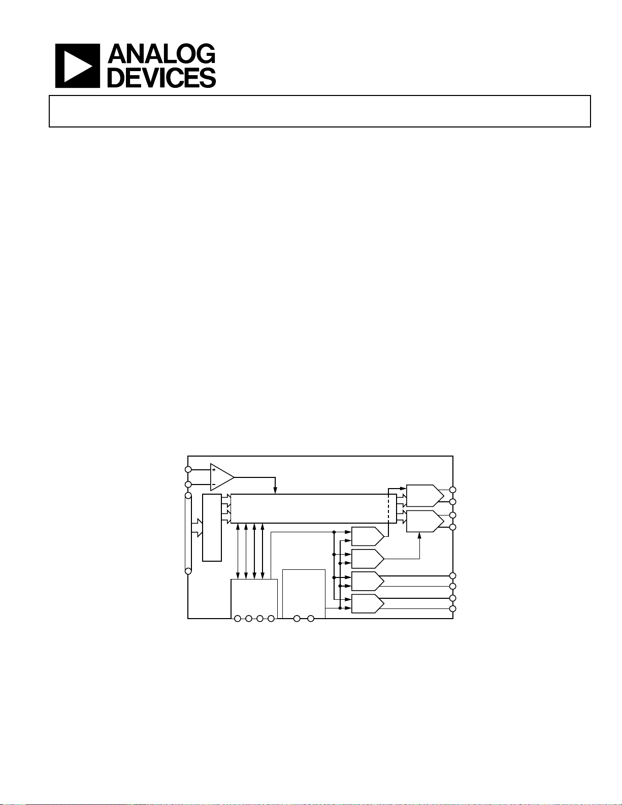
FUNCTIONAL BLOCK DIAGRAM
CLKP
CLKN
LVDS
INTERFACE
D[15:0]
, V
V
IA
IB
DEINTERLEAVING
LOGIC
SERIAL
PERIPHERAL
INTERFACE
SDO
SDIO
SCLK
Rev. A
Information furnished by Analog Devices is believed to be accurate and reliable. However, no
responsibility is assumed by Analog Devices for its use, nor for any infringements of patents or other
rights of third parties that may result from its use. Specifications subject to change without notice. No
license is granted by implication or otherwise under any patent or patent rights of Analog Devices.
Trademarks and registered trademarks are the property of their respective owners.
AD9783 DUAL LVDS DAC
INTERFACE LOGIC
INTERNAL
REFERENCE
AND
BIAS
CSB
REFIO
Figure 1.
16-BIT
I DAC
16-BIT
GAIN
DAC
GAIN
DAC
OFFSET
DAC
OFFSET
DAC
RESET
One Technology Way, P.O. Box 9106, Norwood, MA 02062-9106, U.S.A.
Tel: 781.329.4700 www.analog.com
Fax: 781.461.3113 ©2007–2008 Analog Devices, Inc. All rights reserved.
Q DAC
IOUT1P
IOUT1N
IOUT2P
IOUT2N
AUX1P
AUX1N
AUX2P
AUX2N
06936-001

AD9780/AD9781/AD9783
TABLE OF CONTENTS
Features .............................................................................................. 1
Applications ....................................................................................... 1
General Description ......................................................................... 1
Product Highlights ........................................................................... 1
Functional Block Diagram .............................................................. 1
Revision History ............................................................................... 2
Specifications ..................................................................................... 3
DC Specifications ......................................................................... 3
Digital Specifications ................................................................... 4
AC Specifications .......................................................................... 4
Absolute Maximum Ratings ............................................................ 5
Thermal Resistance ...................................................................... 5
ESD Caution .................................................................................. 5
Pin Configurations and Function Descriptions ........................... 6
Typical Performance Characteristics ............................................. 9
Terminology .................................................................................... 17
Theory of Operation ...................................................................... 18
Serial Peripheral Interface ......................................................... 18
General Operation of the Serial Interface ............................... 18
Instruction Byte .......................................................................... 18
MSB/LSB Transfers .................................................................... 19
Serial Interface Port Pin Descriptions ..................................... 19
SPI Register Map ............................................................................ 20
SPI Register Descriptions .............................................................. 21
SPI Port, RESET, and Pin Mode ............................................... 23
Parallel Data Port Interface ........................................................... 24
Optimizing the Parallel Port Timing ....................................... 24
Driving the CLK Input .............................................................. 26
Full-Scale Current Generation ................................................. 26
DAC Transfer Function ............................................................. 27
Analog Modes of Operation ..................................................... 27
Power Dissipation....................................................................... 29
Evaluation Board Schematics ........................................................ 30
Outline Dimensions ....................................................................... 35
Ordering Guide .......................................................................... 35
REVISION HISTORY
6/08—Rev. 0 to Rev. A
Changed Maximum Sample Rate to 500 MHz Throughout ....... 1
Changes to Table 3 ............................................................................ 4
Changes to Building the Array Section ....................................... 25
Changes to Determining the SMP Value Section ....................... 25
Added Evaluation Board Schematics Section ............................. 30
Updated Outline Dimensions ....................................................... 35
11/07—Revision 0: Initial Version
Rev. A | Page 2 of 36

AD9780/AD9781/AD9783
SPECIFICATIONS
DC SPECIFICATIONS
T
to T
MIN
otherwise noted.
Table 1.
AD9780 AD9781 AD9783
Parameter Min Typ Max Min Typ Max Min Typ Max Unit
RESOLUTION 12 14 16 Bits
ACCURACY
Differential Nonlinearity (DNL) ±0.13 ±0.5 ±2 LSB
Integral Nonlinearity (INL) ±0.25 ±1 ±4 LSB
MAIN DAC OUTPUTS
Offset Error –0.001 0 +0.001 –0.001 0 +0.001 –0.001 0 +0.001 % FSR
Gain Error (with Internal Reference) ±2 ±2 ±2 % FSR
Full-Scale Output Current
Output Compliance Range –1.0 +1.0 –1.0 +1.0 –1.0 +1.0 V
Output Resistance 10 10 10 MΩ
Main DAC Monotonicity Guaranteed
MAIN DAC TEMPERATURE DRIFT
Offset 0.04 0.04 0.04 ppm/°C
Gain 100 100 100 ppm/°C
Reference Voltage 30 30 30 ppm/°C
AUX DAC OUTPUTS
Resolution 10 10 10 Bits
Full-Scale Output Current –2 +2 –2 +2 –2 +2 mA
Output Compliance Range (Source) 0 1.6 0 1.6 0 1.6 V
Output Compliance Range (Sink) 0.8 1.6 0.8 1.6 0.8 1.6 V
Output Resistance 1 1 1 MΩ
AUX DAC Monotonicity Guaranteed
REFERENCE
Internal Reference Voltage 1.2 1.2 1.2 V
Output Resistance 5 5 5 kΩ
ANALOG SUPPLY VOLTAGES
AVDD33 3.13 3.3 3.47 3.13 3.3 3.47 3.13 3.3 3.47 V
CVDD18 1.70 1.8 1.90 1.70 1.8 1.90 1.70 1.8 1.90 V
DIGITAL SUPPLY VOLTAGES
DVDD33 3.13 3.3 3.47 3.13 3.3 3.47 3.13 3.3 3.47 V
DVDD18 1.70 1.8 1.90 1.70 1.8 1.90 1.70 1.8 1.90 V
POWER CONSUMPTION
f
DAC
f
DAC
Power-Down Mode 3 5 3 5 3 35 mW
SUPPLY CURRENTS
AVDD33 55 58 55 58 55 58 mA
CVDD18 34 38 34 38 34 38 mA
DVDD33 13 15 13 15 13 15 mA
DVDD18 68 85 68 85 68 85 mA
1
Based on a 10 kΩ external resistor.
2
f
= 500 MSPS, f
DAC
, AVDD33 = 3.3 V, DVDD33 = 3.3 V, DVDD18 = 1.8 V, CVDD18 = 1.8 V, I
MAX
1
8.66 20.2 31.66 8.66 20.2 31.66 8.66 20.2 31.66 mA
= 20 mA maximum sample rate, unless
OUTFS
= 500 MSPS, IF = 20 MHz V × I V × I V × I V × I V × I V × I mW
= 500 MSPS, IF = 10 MHz 440 440 440 mW
2
= 20 MHz.
OUT
Rev. A | Page 3 of 36

AD9780/AD9781/AD9783
DIGITAL SPECIFICATIONS
T
to T
MIN
, AVDD33 = 3.3 V, DVDD33 = 3.3 V, DVDD18 = 1.8 V, CVDD18 = 1.8 V, I
MAX
otherwise noted.
Table 2.
Parameter Min Typ Max Unit
DAC CLOCK INPUT (CLKP, CLKN)
Peak-to-Peak Voltage at CLKP and CLKN 400 800 1600 mV
Common-Mode Voltage 300 400 500 mV
Maximum Clock Rate 500 MSPS
SERIAL PERIPHERAL INTERFACE (CMOS INTERFACE)
Maximum Clock Rate (SCLK) 40 MHz
Minimum Pulse Width High 12.5 ns
Minimum Pulse Width Low 12.5 ns
DIGITAL INPUT DATA (LVDS INTERFACE)
Input Voltage Range, VIA or VIB 800 1600 mV
Input Differential Threshold, V
Input Differential Hysteresis, V
−100 +100 mV
IDTH
IDTHH
to V
20 mV
IDTHL
Input Differential Input Impedance, RIN 80 120 Ω
Maximum LVDS Input Rate (per DAC) 500 MSPS
= 20 mA maximum sample rate, unless
OUTFS
AC SPECIFICATIONS
T
to T
MIN
otherwise noted.
Table 3.
Parameter
SPURIOUS FREE DYNAMIC RANGE (SFDR)
f
DAC
f
DAC
f
DAC
f
DAC
TWO-TONE INTERMODULATION DISTORTION (IMD)
f
DAC
f
DAC
f
DAC
f
DAC
ONE-TONE NOISE SPECTRAL DENSITY (NSD)
f
DAC
f
DAC
f
DAC
f
DAC
W-CDMA ADJACENT CHANNEL LEAKAGE RATIO (ACLR),
SINGLE CARRIER
f
DAC
f
DAC
f
DAC
f
DAC
, AVDD33 = 3.3 V, DVDD33 = 3.3 V, DVDD18 = 1.8 V, CVDD18 = 1.8 V, I
MAX
AD9780 AD9781 AD9783
= 500 MSPS, f
= 500 MSPS, f
= 500 MSPS, f
= 500 MSPS, f
= 500 MSPS, f
= 500 MSPS, f
= 500 MSPS, f
= 500 MSPS, f
= 500 MSPS, f
= 500 MSPS, f
= 500 MSPS, f
= 500 MSPS, f
= 20 MHz 79 78 80 dBc
OUT
= 120 MHz 67 66 68 dBc
OUT
= 380 MHz (Mix Mode) 55 58 62 dBc
OUT
= 480 MHz (Mix Mode) 58 62 59 dBc
OUT
= 20 MHz 91 93 86 dBc
OUT
= 120 MHz 80 75 79 dBc
OUT
= 380 MHz (Mix Mode) 69 70 64 dBc
OUT
= 480 MHz (Mix Mode) 60.5 61.5 66 dBc
OUT
= 40 MHz −157 −162 −165 dBc
OUT
= 120 MHz −154.5 −156.5 −157 dBc
OUT
= 380 MHz (Mix Mode) −153 −153 −154 dBc
OUT
= 480 MHz (Mix Mode) −152 −152 −153 dBc
OUT
= 491.52 MSPS, f
= 491.52 MSPS, f
= 491.52 MSPS, f
= 491.52 MSPS, f
= 20 MHz −81 −82.5 −82 dBc
OUT
= 80 MHz −80 −82.5 −81 dBc
OUT
= 411.52 MHz −71 −68 −69 dBc
OUT
= 471.52 MHz −69 −69 −70 dBc
OUT
= 20 mA, maximum sample rate, unless
OUTFS
Unit Min Typ Max Min Typ Max Min Typ Max
Rev. A | Page 4 of 36
AD9780/AD9781/AD9783
ABSOLUTE MAXIMUM RATINGS
Table 4.
With
Parameter
AVDD33, DVDD33 AGND, DGND, CGND −0.3 V to +3.6 V
DVDD18, CVDD18 AGND, DGND, CGND −0.3 V to +1.98 V
AGND DGND, CGND −0.3 V to +0.3 V
DGND AGND, CGND −0.3 V to +0.3 V
CGND AGND, DGND −0.3 V to +0.3 V
REFIO AGND
IOUT1P, IOUT1N,
IOUT2P, IOUT2N,
AUX1P, AUX1N,
AUX2P, AUX2N
D15 to D0 DGND
CLKP, CLKN CGND
CSB, SCLK, SDIO, SDO DGND
Junction Temperature +125°C
Storage Temperature −65°C to +150°C
Respect to
AGND
Rating
−0.3 V to
AVDD33 + 0.3 V
−1.0 V to
AVDD33 + 0.3 V
−0.3 V to
DVDD33 + 0.3 V
−0.3 V to
CVDD18 + 0.3 V
–0.3 V to
DVDD33 + 0.3 V
THERMAL RESISTANCE
Thermal resistance is tested using a JEDEC standard 4-layer
thermal test board with no airflow.
Table 5.
Package Type θJA Unit
CP-72-1 (Exposed Pad Soldered to PCB) 25 °C/W
Stresses above those listed under Absolute Maximum Ratings
may cause permanent damage to the device. This is a stress
rating only; functional operation of the device at these or any
other conditions above those indicated in the operational
section of this specification is not implied. Exposure to absolute
maximum rating conditions for extended periods may affect
device reliability.
ESD CAUTION
Rev. A | Page 5 of 36
AD9780/AD9781/AD9783
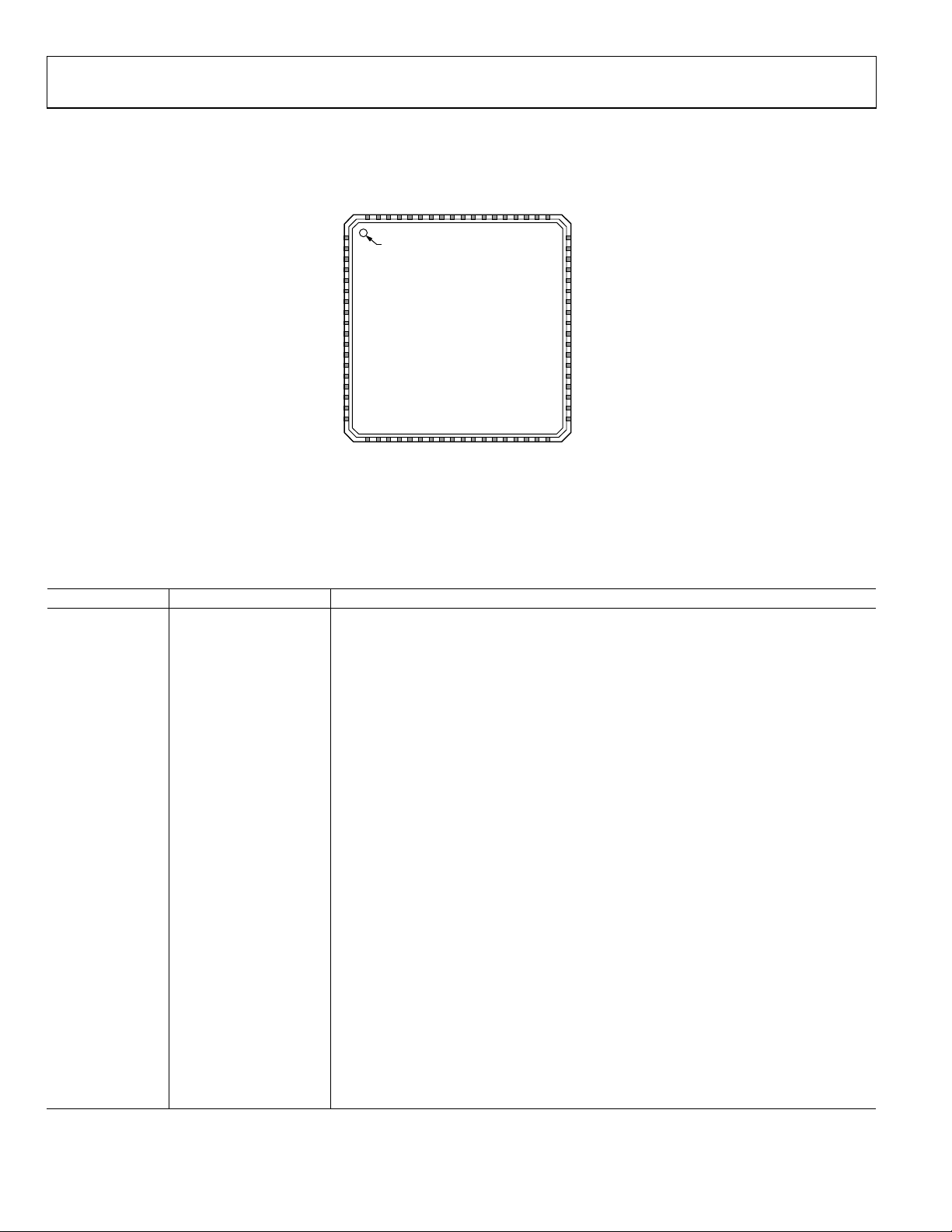
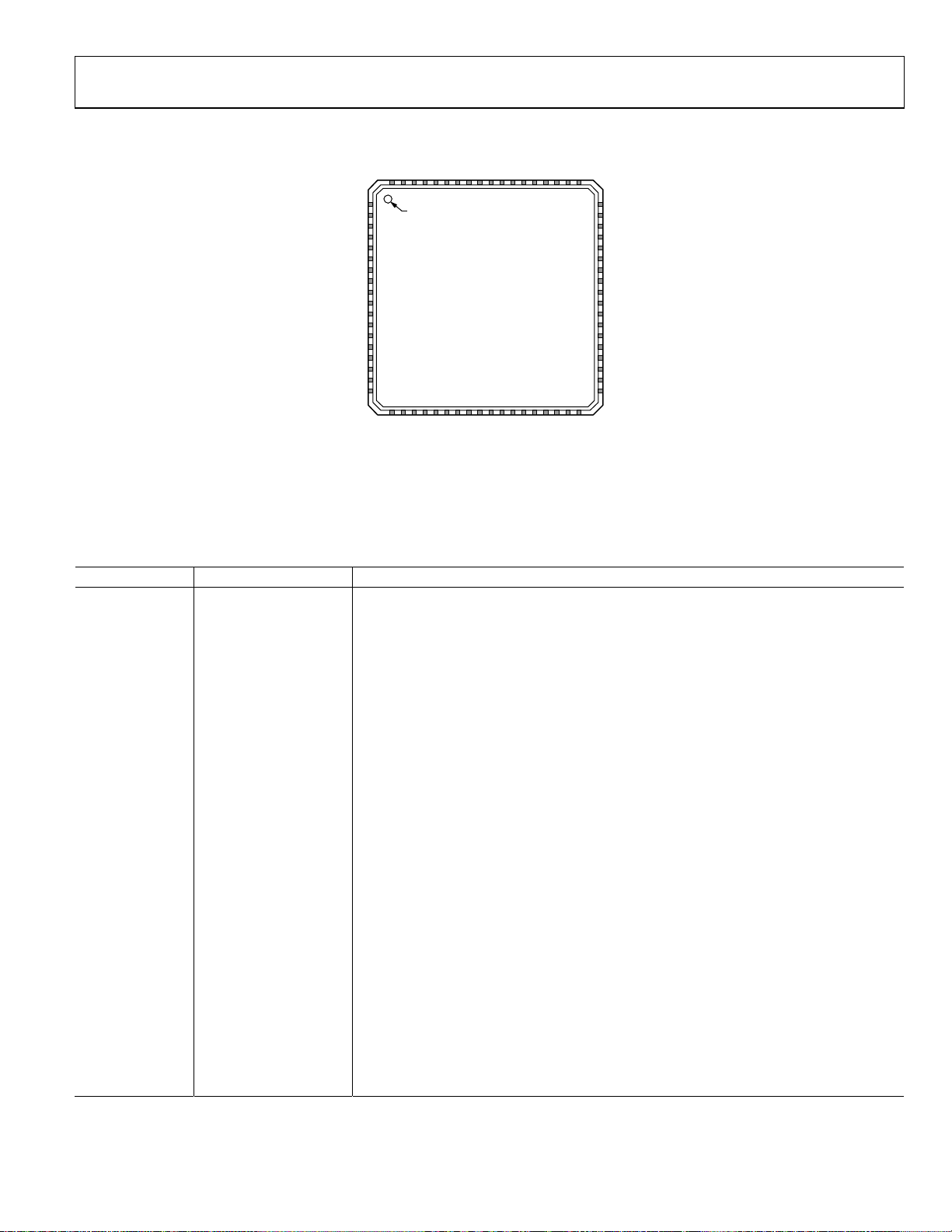
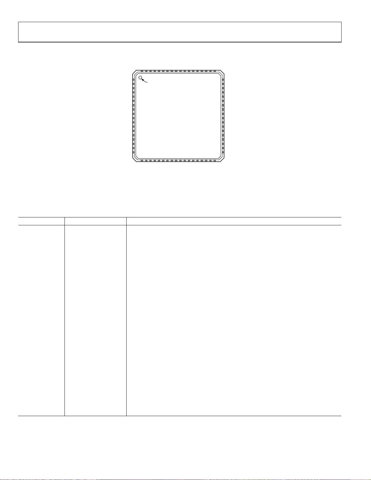
PIN CONFIGURATIONS AND FUNCTION DESCRIPTIONS
AVD D33
AVD D33
AVS S
IOUT1P
IOUT1N
AVS S
AUX1P
AUX1N
AVS S
AUX2N
AUX2P
AVS S
IOUT2N
IOUT2P
AVS S
AVD D33
AVD D33
REFIO
7271706968676665646362616059585756
1
CVDD18
2
CVSS
3
CLKP
4
CLKN
5
CVSS
6
CVDD18
7
DVSS
8
DVDD18
9
D11P
10
D11N
11
D10P
12
D10N
13
D9P
14
D9N
15
D8P
16
D8N
17D7P
18D7N
NOTES
1. NC = NO CO NNECT
2. EXPOSED PAD MUST BE
SOLDERED TO PCB AND
CONNECTED TO AVSS.
PIN 1
INDICATOR
192021222324252627282930313233
D6P
D5P
D6N
Figure 2. AD9780 Pin Configuration
D5N
D4P
D4N
AD9780
(TOP VIEW)
DVSS
DCOP
DCON
DVDD33
D3P
DCIP
DCIN
55
54
FS ADJ
53
RESET
52
CSB
51
SCLK
50
SDIO
49
SDO
48
DVSS
47
DVDD18
46
NC
45
NC
44
NC
43
NC
42
NC
41
NC
40
NC
39
NC
38
D0N
37
D0P
35D1P
36D1N
34
D2P
D3N
D2N
06936-002
Table 6. AD9780 Pin Function Descriptions
Pin No. Mnemonic Description
1, 6 CVDD18 Clock Supply Voltage (1.8 V).
2, 5 CVSS Clock Supply Return.
3, 4 CLKP, CLKN Differential DAC Sampling Clock Input.
7, 28, 48 DVSS Digital Common.
8, 47 DVDD18 Digital Supply Voltage (1.8 V).
9 to 24, 31 to 38 D11P, D11N to D0P, D0N LVDS Data Inputs. D11 is the MSB, D0 is the LSB.
25, 26 DCOP, DCON Differential Data Clock Output. LVDS clock at the DAC sample rate.
27 DVDD33 Digital Input and Output Pad Ring Supply Voltage (3.3 V).
29, 30 DCIP, DCIN Differential Data Clock Input. LVDS clock aligned with input data.
39 to 46 NC No Connection. Leave these pins floating.
49 SDO Serial Port Data Output.
50 SDIO Serial Port Data Input (4-Wire Mode) or Bidirectional Serial Data Line (3-Wire Mode).
51 SCLK Serial Port Clock Input.
52 CSB Serial Port Chip Select (Active Low).
53 RESET Chip Reset (Active High).
54 FS ADJ Full-Scale Current Output Adjust.
55 REFIO Analog Reference Input/Output (1.2 V Nominal).
56, 57, 71, 72 AVDD33 Analog Supply Voltage (3.3 V).
58, 61, 64, 67, 70 AVSS Analog Common.
59 IOUT2P DAC Current Output. Full-scale current is sourced when all data bits are 1s.
60 IOUT2N Complementary DAC Current Output. Full-scale current is sourced when all data bits are 0s.
62, 63 AUX2P, AUX2N Differential Auxiliary DAC Current Output (Channel 2).
65, 66 AUX1N, AUX1P Differential Auxiliary DAC Current Output (Channel 1).
68 IOUT1N Complementary DAC Current Output. Full-scale current is sourced when all data bits are 0s.
69 IOUT1P DAC Current Output. Full-scale current is sourced when all data bits are 1s.
Heat Sink Pad N/A The heat sink pad on the bottom of the package should be soldered to the PCB plane that
carries AVSS.
Rev. A | Page 6 of 36
AD9780/AD9781/AD9783
AVDD33
AVDD33
AVSS
IOUT1P
IOUT1N
AVSS
AUX1P
AUX1N
AVSS
AUX2N
AUX2P
AVSS
IOUT2N
IOUT2P
AVSS
AVDD33
AVDD33
REFIO
7271706968676665646362616059585756
55
CVDD18
CVDD18
DVDD18
NOTES
1. NC = NO CONNECT
2. EXPOSED PAD MUST BE
SOLDERED TO PCB AND
CONNECTED TO AVSS.
CVSS
CLKP
CLKN
CVSS
DVSS
D13P
D13N
D12P
D12N
D11P
D11N
D10P
D10N
1
2
3
4
5
6
7
8
9
10
11
12
13
14
15
16
17D9P
18D9N
PIN 1
INDICATOR
(TOP VIEW)
192021222324252627282930313233
D8P
D7P
D6P
D8N
D7N
D6N
DCOP
AD9781
DCON
DVDD33
FS ADJ
54
RESET
53
CSB
52
SCLK
51
SDIO
50
SDO
49
DVSS
48
DVDD18
47
NC
46
NC
45
NC
44
NC
43
D0N
42
D0P
41
D1N
40
D1P
39
D2N
38
D2P
37
34
35D3P
36D3N
D5P
D4P
D5N
DCIP
DVSS
D4N
DCIN
06936-003
Figure 3. AD9781 Pin Configuration
Table 7. AD9781 Pin Function Descriptions
Pin No. Mnemonic Description
1, 6 CVDD18 Clock Supply Voltage (1.8 V).
2, 5 CVSS Clock Supply Return.
3, 4 CLKP, CLKN Differential DAC Sampling Clock Input.
7, 28, 48 DVSS Digital Common.
8, 47 DVDD18 Digital Supply Voltage (1.8 V).
9 to 24, 31 to 42 D13P, D13N to D0P, D0N LVDS Data Inputs. D13 is the MSB, D0 is the LSB.
25, 26 DCOP, DCON Differential Data Clock Output. LVDS clock at the DAC sample rate.
27 DVDD33 Digital Input and Output Pad Ring Supply Voltage (3.3 V).
29, 30 DCIP, DCIN Differential Data Clock Input. LVDS clock aligned with input data.
43 to 46 NC No Connection. Leave these pins floating.
49 SDO Serial Port Data Output.
50 SDIO Serial Port Data Input (4-Wire Mode) or Bidirectional Serial Data Line (3-Wire Mode).
51 SCLK Serial Port Clock Input.
52 CSB Serial Port Chip Select (Active Low).
53 RESET Chip Reset (Active High).
54 FS ADJ Full-Scale Current Output Adjust.
55 REFIO Analog Reference Input/Output (1.2 V Nominal).
56, 57, 71, 72 AVDD33 Analog Supply Voltage (3.3 V).
58, 61, 64, 67, 70 AVSS Analog Common.
59 IOUT2P DAC Current Output. Full-scale current is sourced when all data bits are 1s.
60 IOUT2N Complementary DAC Current Output. Full-scale current is sourced when all data bits are 0s.
62, 63 AUX2P, AUX2N Differential Auxiliary DAC Current Output (Channel 2).
65, 66 AUX1N, AUX1P Differential Auxiliary DAC Current Output (Channel 1).
68 IOUT1N Complementary DAC Current Output. Full-scale current is sourced when all data bits are 0s.
69 IOUT1P DAC Current Output. Full-scale current is sourced when all data bits are 1s.
Heat Sink Pad N/A
The heat sink pad on the bottom of the package should be soldered to the PCB plane that
carries AVSS.
Rev. A | Page 7 of 36
AD9780/AD9781/AD9783
AVDD33
AVDD33
AVSS
IOUT1P
IOUT1N
AVSS
AUX1P
AUX1N
AVSS
AUX2N
AUX2P
AVSS
IOUT2N
IOUT2P
AVSS
AVDD33
AVDD33
REFIO
7271706968676665646362616059585756
55
CVDD18
CVDD18
DVDD18
NOTES
1. EXPOSED PAD MUST BE
SOLDERED TO PCB AND
CONNECTED TO AVSS.
CVSS
CLKP
CLKN
CVSS
DVSS
D15P
D15N
D14P
D14N
D13P
D13N
D12P
D12N
1
2
3
4
5
6
7
8
9
10
11
12
13
14
15
16
17D11P
18D11N
PIN 1
INDICATOR
(TOP VIEW)
192021222324252627282930313233
D9P
D8P
D9N
D10P
D8N
D10N
AD9783
DCOP
DCON
DVDD33
FS ADJ
54
RESET
53
CSB
52
SCLK
51
SDIO
50
SDO
49
DVSS
48
DVDD18
47
D0N
46
D0P
45
D1N
44
D1P
43
D2N
42
D2P
41
D3N
40
D3P
39
D4N
38
D4P
37
34
35D5P
36D5N
D7P
D6P
D7N
DCIP
DVSS
D6N
DCIN
06936-004
Figure 4. AD9783 Pin Configuration
Table 8. AD9783 Pin Function Descriptions
Pin No. Mnemonic Description
1, 6 CVDD18 Clock Supply Voltage (1.8 V).
2, 5 CVSS Clock Supply Return.
3, 4 CLKP, CLKN Differential DAC Sampling Clock Input.
7, 28, 48 DVSS Digital Common.
8, 47 DVDD18 Digital Supply Voltage (1.8 V).
9 to 24, 31 to 46 D15P, D15N to D0P, D0N LVDS Data Inputs. D15 is the MSB, D0 is the LSB.
25, 26 DCOP, DCON Differential Data Clock Output. LVDS clock at the DAC sample rate.
27 DVDD33 Digital Input and Output Pad Ring Supply Voltage (3.3 V).
29, 30 DCIP, DCIN Differential Data Clock Input. LVDS clock aligned with input data.
49 SDO Serial Port Data Output.
50 SDIO Serial Port Data Input (4-Wire Mode) or Bidirectional Serial Data Line (3-Wire Mode).
51 SCLK Serial Port Clock Input.
52 CSB Serial Port Chip Select (Active Low).
53 RESET Chip Reset (Active High).
54 FS ADJ Full-Scale Current Output Adjust.
55 REFIO Analog Reference Input/Output (1.2 V Nominal).
56, 57, 71, 72 AVDD33 Analog Supply Voltage (3.3 V).
58, 61, 64, 67, 70 AVSS Analog Common.
59 IOUT2P DAC Current Output. Full-scale current is sourced when all data bits are 1s.
60 IOUT2N Complementary DAC Current Output. Full-scale current is sourced when all data bits are 0s.
62, 63 AUX2P, AUX2N Differential Auxiliary DAC Current Output (Channel 2).
65, 66 AUX1N, AUX1P Differential Auxiliary DAC Current Output (Channel 1).
68 IOUT1N Complementary DAC Current Output. Full-scale current is sourced when all data bits are 0s.
69 IOUT1P DAC Current Output. Full-scale current is sourced when all data bits are 1s.
Heat Sink Pad N/A
The heat sink pad on the bottom of the package should be soldered to the PCB plane that
carries AVSS.
Rev. A | Page 8 of 36
AD9780/AD9781/AD9783
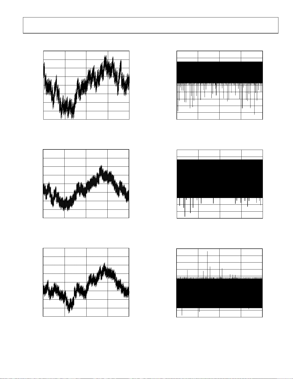
TYPICAL PERFORMANCE CHARACTERISTICS
1.5
1.0
0.5
0
–0.5
LSB
–1.0
–1.5
–2.0
–2.5
0 32,76816,384 65,535
CODE
49,152
Figure 5. AD9783 INL, TA = 85°C, FS = 20 mA
06936-005
0.4
0.2
0
–0.2
–0.4
–0.6
LSB
–0.8
–1.0
–1.2
–1.4
–1.6
0
32,76816,384 65,53549,152
CODE
06936-008
Figure 8. AD9783 DNL, TA = 85°C, FS = 20 mA
5
4
3
2
1
LSB
0
–1
–2
–3
0
32,76816,384 65,53549,152
CODE
06936-006
Figure 6. AD9783 INL, TA = 25°C, FS = 20 mA
5
4
3
2
1
LSB
0
–1
–2
–3
0
32,76816,384 65,53549,152
CODE
06936-007
Figure 7. AD9783 INL, TA = −40°C, FS = 20 mA
0.4
0.2
0
–0.2
–0.4
–0.6
LSB
–0.8
–1.0
–1.2
–1.4
–1.6
0
32,76816,384 65,53549,152
CODE
Figure 9. AD9783 DNL, TA = 25°C, FS = 20 mA
1.0
0.8
0.6
0.4
0.2
0
LSB
–0.2
–0.4
–0.6
–0.8
–1.0
0
32,76816,384 65,53549,152
CODE
Figure 10. AD9783 DNL, TA = −40°C, FS = 20 mA
06936-009
06936-010
Rev. A | Page 9 of 36
AD9780/AD9781/AD9783
0.4
0.3
0.2
0.1
0
–0.1
LSB
–0.2
–0.3
–0.4
–0.5
–0.6
40960 8192 12,288 16, 383
CODE
06936-011
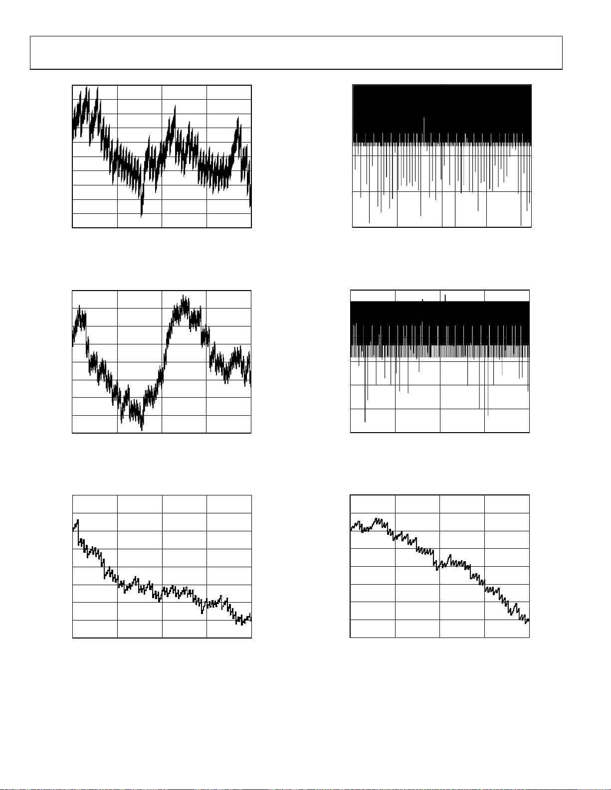
Figure 11. AD9781 INL, TA = 85°C, FS = 20 mA
0.059
–0.060
–0.179
LSB
–0.297
–0.416
40960 8192 12,288 16, 383
CODE
Figure 14. AD9781 DNL, TA = 85°C, FS = 20 mA
06936-014
0.6
0.4
0.2
0
–0.2
LSB
–0.4
–0.6
–0.8
–1.0
0 4096 8192 12288 16,383
CODE
Figure 12. AD9781 INL, TA = −40°C, FS = 20 mA
0.2
0.1
0
–0.1
–0.2
LSB
–0.3
–0.4
0.1
0
–0.1
–0.2
LSB
–0.3
–0.4
–0.5
0 16,383
06936-012
4096 8192 12,288
CODE
06936-015
Figure 15. AD9781 DNL, TA = −40°C, FS = 20 mA
0.2
0.1
0
–0.1
–0.2
LSB
–0.3
–0.4
–0.5
–0.6
0 1024 2048 3072 4096
CODE
Figure 13. AD9780 INL, TA = −40°C, FS = 20 mA
06936-013
Rev. A | Page 10 of 36
–0.5
–0.6
0
1024 2048 3072 4096
CODE
Figure 16. AD9780 INL, TA = 85°C, FS = 20 mA
06936-016
AD9780/AD9781/AD9783
90
85
80
75
70
65
60
SFDR (dBc)
55
50
45
40
0 50 100 150 200 250 300 350 400 450 500
250MSPS
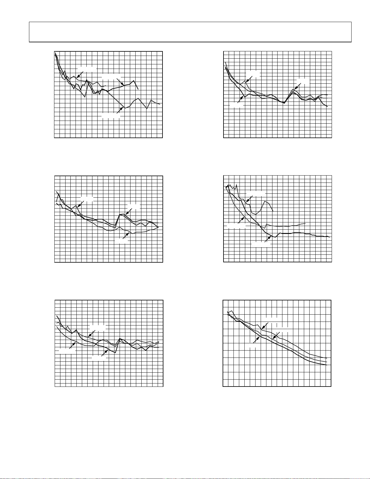
Figure 17. AD9783 SFDR vs. f
100
95
90
85
80
75
70
65
SFDR (dBc)
60
55
50
45
40
0 25 50 75 100 125 150 175 200 225 250
Figure 18. AD9783 SFDR vs. f
400MSPS
500MSPS
f
(MHz)
OUT
Over f
OUT
in Baseband and Mix Modes,
DAC
FS = 20 mA
20mA
30mA
10mA
f
(MHz)
OUT
Over Analog Output, TA = 25°C, at 500 MSPS
OUT
100
95
90
85
80
75
70
65
SFDR (dBc)
60
55
50
45
40
0 25 50 75 100 125 150 175 200 225 250
06936-017
Figure 20. AD9783 SFDR vs. f
100
95
90
85
80
75
70
400MSPS
IMD (dBc)
65
60
55
50
45
8
1
0
6
3
9
6
0
40
0 50 100 150 200 500250 300 350 40 0 450
Figure 21. AD9783 IMD vs. f
+85°C
+25°C
–40°C
f
(MHz)
OUT
Over Temperature, at 500 MSPS, FS = 20 mA
OUT
250MSPS
500MSPS
f
(MHz)
OUT
Over f
OUT
in Baseband and Mix Modes,
DAC
06936-020
06936-021
FS = 20 mA
100
95
90
85
80
75
70
65
–6dBFS
SFDR (dBc)
60
55
50
45
40
0 25 50 75 100 125 150 175 200 225 250
Figure 19. AD9783 SFDR vs. f
T
–3dBFS
0dBFS
f
(MHz)
OUT
Over Digital Input Level,
= 25°C, at 500 MSPS, FS = 20 mA
A
OUT
06936-019
Figure 22. AD9783 IMD vs. f
Rev. A | Page 11 of 36
100
95
90
85
80
75
70
IMD (dBc)
65
60
55
50
45
40
0 25 50 75 100 125 150 175 200 225 250
30mA
10mA
20mA
f
(MHz)
OUT
Over Analog Output, TA = 25°C, at 500 MSPS
OUT
06936-022
 Loading...