

16-Bit, 100 kSPS/200 kSPS
a
FEATURES
Fast 16-Bit ADC
100 kSPS Throughput Rate—AD977
200 kSPS Throughput Rate—AD977A
Single 5 V Supply Operation
Power Dissipation 100 mW Max
Power-Down Mode 50 W
Input Ranges:
Unipolar; 0 V–10 V, 0 V–5 V and 0 V–4 V
Bipolar; 10 V, 5 V and 3.3 V
Choice of External or Internal 2.5 V Reference
High Speed Serial Interface
On-Chip Clock
20-Lead Skinny DIP or SOIC Package
28-Lead Skinny SSOP Package
GENERAL DESCRIPTION
The AD977/AD977A is a high speed, low power 16-bit A/D
converter that operates from a single 5 V supply. The AD977A
has a throughput rate of 200 kSPS whereas the AD977 has a
throughput rate of 100 kSPS. Each part contains a successive
approximation, switched capacitor ADC, an internal 2.5 V
reference, and a high speed serial interface. The ADC is factory
calibrated to minimize all linearity errors. The AD977/AD977A is
specified for full scale bipolar input ranges of ±10 V, ±5 V and
± 3.3 V, and unipolar ranges of 0 V to 10 V, 0 V to 5 V and
0 V to 4 V.
The AD977/AD977A is comprehensively tested for ac parameters such as SNR and THD, as well as the more traditional dc
parameters of offset, gain and linearity.
BiCMOS A/D Converter
AD977/AD977A
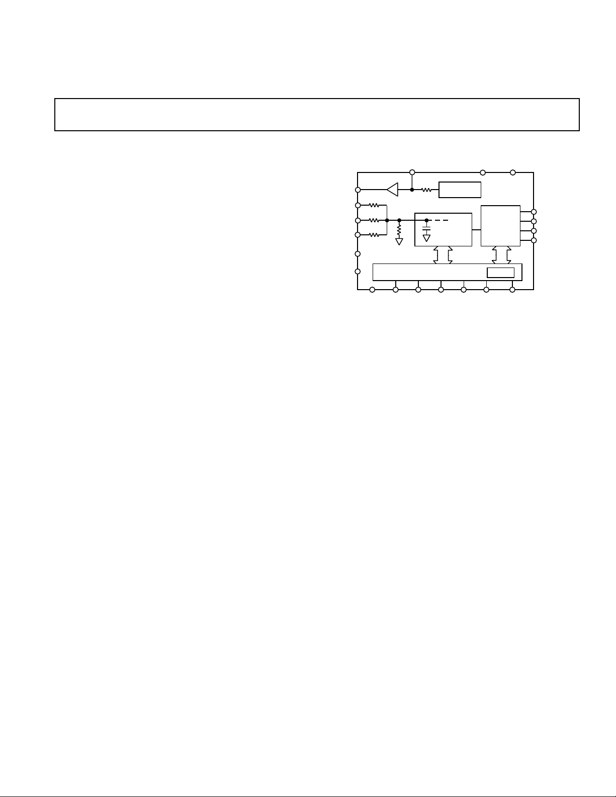
FUNCTIONAL BLOCK DIAGRAM
2.5V
V
AGND1
ANA
AD977/
AD977A
SERIAL
DATA
INTERFACE
CLOCK
SB/BTC EXT/INT
SYNC
BUSY
DATACLK
DATA
REF
CAP
4R
R1
IN
2R
R2
IN
R3
AGND2
V
R
IN
R = 5k AD977
R = 2.5k AD977A
DIG
INTERNAL CALIBRATION CIRCUITRY
DGND TAGR/CCS
PWRD
4k
REFERENCE
4R
CONTROL LOGIC &
SWITCHED
CAP ADC
PRODUCT HIGHLIGHTS
1. Fast Throughput
The AD977/AD977A is a high speed, 16-bit ADC based on
a factory calibrated switched capacitor architecture.
2. Single-Supply Operation
The AD977/AD977A operates from a single 5 V supply and
dissipates only 100 mW max.
3. Comprehensive DC and AC Specifications
In addition to the traditional specifications of offset, gain
and linearity, the AD977/AD977A is fully tested for SNR
and THD.
REV. D
Information furnished by Analog Devices is believed to be accurate and
reliable. However, no responsibility is assumed by Analog Devices for its
use, nor for any infringements of patents or other rights of third parties
which may result from its use. No license is granted by implication or
otherwise under any patent or patent rights of Analog Devices.
One Technology Way, P.O. Box 9106, Norwood, MA 02062-9106, U.S.A.
Tel: 781/329-4700 World Wide Web Site: http://www.analog.com
Fax: 781/326-8703 © Analog Devices, Inc., 2000

AD977/AD977A
AD977–SPECIFICATIONS
(–40C to +85C, FS = 100 kHz, V
DIG
= V
= 5 V, unless otherwise noted)
ANA
A Grade B Grade C Grade
Parameter Min Typ Max Min Typ Max Min Typ Max Unit
RESOLUTION 16 16 16 Bits
ANALOG INPUT
Voltage Range ±10 V, 0 V to 5 V, . . . (See Table II)
Impedance See Table II
Sampling Capacitance 40 40 40 pF
THROUGHPUT SPEED
Complete Cycle 10 10 10 µs
Throughput Rate 100 100 100 kHz
DC ACCURACY
Integral Linearity Error ± 3 ± 2.0 ± 3 LSB
1
Differential Linearity Error –2 +3 –1 +1.75 ± 2 LSB
No Missing Codes 15 16 15 Bits
Transition Noise
Full-Scale Error
3, 4
2
1.0 1.0 1.0 LSB
± 0.5 ± 0.25 ± 0.5 %
Full-Scale Error Drift ±7 ±7 ± 7 ppm/°C
Full-Scale Error
Ext. REF = 2.5 V ± 0.5 ± 0.25 ± 0.5 %
Full-Scale Error Drift
Ext. REF = 2.5 V ± 2 ± 2 ± 2 ppm/°C
Bipolar Zero Error
3
Bipolar Ranges ± 10 ± 10 ± 15 mV
Bipolar Zero Error Drift
Bipolar Ranges ±2 ±2 ±2 ppm/°C
Unipolar Zero Error
3
Unipolar Ranges ± 10 ± 10 ± 10 mV
Unipolar Zero Error Drift
Unipolar Ranges ± 2 ± 2 ± 2 ppm/°C
Recovery to Rated Accuracy
After Power-Down
5
2.2 µF to CAP 1 1 1 ms
Power Supply Sensitivity
V
= V
ANA
AC ACCURACY
Spurious Free Dynamic Range
Total Harmonic Distortion
Signal-to-(Noise+Distortion)
–60 dB Input 27 28 27 dB
Signal-to-Noise
Full Power Bandwidth
= VD = 5 V ± 5% ± 8 ± 8 ± 8 LSB
DIG
6
6
6
6
8
90 96 90 dB
–90 –96 –90 dB
83 85 83 dB
83 85 83 dB
700 700 700 kHz
7
–3 dB Input Bandwidth 1.5 1.5 1.5 MHz
SAMPLING DYNAMICS
Aperture Delay 40 40 40 ns
Transient Response, Full-Scale Step 2 2 2 µs
Overvoltage Recovery
9
150 150 150 ns
REFERENCE
Internal Reference Voltage 2.48 2.5 2.52 2.48 2.5 2.52 2.48 2.5 2.52 V
Internal Reference Source Current 1 1 1 µA
External Reference Voltage Range
for Specified Linearity 2.3 2.5 2.7 2.3 2.5 2.7 2.3 2.5 2.7 V
External Reference Current Drain
Ext. REF = 2.5 V 100 100 100 µA
NOTES
1
LSB means Least Significant Bit. With a ± 10 V input, one LSB is 305 µV.
2
Typical rms noise at worst case transitions and temperatures.
3
Measured with fixed resistors as shown in Figures 11, 12 and 13. Adjustable to zero. Tested at room temperature.
4
Full-Scale Error is expressed as the % difference between the actual full-scale code transition voltage and the ideal full scale transition voltage, and includes the effect of offset
error. For bipolar input ranges, the Full-Scale Error is the worst case of either the –Full Scale or +Full Scale code transition voltage errors. For unipolar input ranges, Full-Scale
Error is with respect to the +Full-Scale code transition voltage.
5
External 2.5 V reference connected to REF.
6
fIN = 20 kHz, 0.5 dB down unless otherwise noted.
7
All specifications in dB are referred to a full scale ± 10 V input.
8
Full-Power Bandwidth is defined as full-scale input frequency at which Signal-to-(Noise+Distortion) degrades to 60 dB, or 10 bits of accuracy.
9
Recovers to specified performance after a 2 × FS input overvoltage.
Specifications subject to change without notice.
–2–
REV. D

AD977/AD977A
AD977A–SPECIFICATIONS
(–40C to +85C, FS = 200 kHz, V
DIG
= V
= 5 V, unless otherwise noted)
ANA
A Grade B Grade C Grade
Parameter Min Typ Max Min Typ Max Min Typ Max Unit
RESOLUTION 16 16 16 Bits
ANALOG INPUT
Voltage Range ±10 V, 0 V to 5 V, . . . (See Table II)
Impedance See Table II
Sampling Capacitance 40 40 40 pF
THROUGHPUT SPEED
Complete Cycle 5 5 5 µs
Throughput Rate 200 200 200 kHz
DC ACCURACY
Integral Linearity Error ± 3 ± 2.0 ± 3 LSB
1
Differential Linearity Error –2 +3 –1 +1.75 ± 2LSB
No Missing Codes 15 16 15 Bits
Transition Noise
Full-Scale Error
3, 4
2
1.0 1.0 1.0 LSB
± 0.5 ± 0.25 ± 0.5 %
Full-Scale Error Drift ±7 ±7 ± 7 ppm/°C
Full-Scale Error
Ext. REF = 2.5 V ± 0.5 ± 0.25 ± 0.5 %
Full-Scale Error Drift
Ext. REF = 2.5 V ± 2 ± 2 ± 2 ppm/°C
Bipolar Zero Error
3
Bipolar Ranges ± 10 ± 10 ± 15 mV
Bipolar Zero Error Drift
Bipolar Ranges ±2 ±2 ±2 ppm/°C
Unipolar Zero Error
3
Unipolar Ranges ± 10 ± 10 ± 10 mV
Unipolar Zero Error Drift
Unipolar Ranges ± 2 ± 2 ± 2 ppm/°C
Recovery to Rated Accuracy
After Power-Down
5
2.2 µF to CAP 1 1 1 ms
Power Supply Sensitivity
V
= V
ANA
AC ACCURACY
Spurious Free Dynamic Range
Total Harmonic Distortion
Signal-to-(Noise+Distortion)
–60 dB Input 27 28 27 dB
Signal-to-Noise
Full Power Bandwidth
= VD = 5 V ± 5% ± 8 ± 8 ± 8LSB
DIG
6
6
6
6
8
90 96 90 dB
–90 –96 –90 dB
83 85 83 dB
83 85 83 dB
1 1 1 MHz
7
–3 dB Input Bandwidth 2.7 2.7 2.7 MHz
SAMPLING DYNAMICS
Aperture Delay 40 40 40 ns
Transient Response, Full-Scale Step 1 1 1 µs
Overvoltage Recovery
9
150 150 150 ns
REFERENCE
Internal Reference Voltage 2.48 2.5 2.52 2.48 2.5 2.52 2.48 2.5 2.52 V
Internal Reference Source Current 1 1 1 µA
External Reference Voltage Range
for Specified Linearity 2.3 2.5 2.7 2.3 2.5 2.7 2.3 2.5 2.7 V
External Reference Current Drain
Ext. REF = 2.5 V 1.2 1.2 1.2 mA
NOTES
1
LSB means Least Significant Bit. With a ± 10 V input, one LSB is 305 µV.
2
Typical rms noise at worst case transitions and temperatures.
3
Measured with fixed resistors as shown in Figures 11, 12 and 13. Adjustable to zero. Tested at room temperature.
4
Full-Scale Error is expressed as the % difference between the actual full-scale code transition voltage and the ideal full scale transition voltage, and includes the effect of offset
error. For bipolar input ranges, the Full-Scale Error is the worst case of either the –Full Scale or +Full Scale code transition voltage errors. For unipolar input ranges, Full-Scale
Error is with respect to the +Full-Scale code transition voltage.
5
External 2.5 V reference connected to REF.
6
fIN = 20 kHz, 0.5 dB down unless otherwise noted.
7
All specifications in dB are referred to a full scale ± 10 V input.
8
Full-Power Bandwidth is defined as full-scale input frequency at which Signal-to-(Noise+Distortion) degrades to 60 dB, or 10 bits of accuracy.
9
Recovers to specified performance after a 2 × FS input overvoltage.
Specifications subject to change without notice.
–3–REV. D

AD977/AD977A–SPECIFICATIONS
(Both Specs)
A, B, C Grades
Parameter Conditions Min Typ Max Unit
DIGITAL INPUTS
Logic Levels
V
IL
V
IH
I
IL
I
IH
–0.3 +0.8 V
2.0 V
+ 0.3 V
DIG
± 10 µA
± 10 µA
DIGITAL OUTPUTS
Data Format Serial 16-Bits
Data Coding Binary Two’s Complement or Straight Binary
Pipeline Delay Conversion Results Only Available after Completed Conversion
I
V
OL
V
OH
= 1.6 mA 0.4 V
SINK
I
= 500 µA4 V
SOURCE
POWER SUPPLIES
Specified Performance
V
V
I
I
DIG
ANA
DIG
ANA
4.75 5 5.25 V
4.75 5 5.25 V
4mA
11 mA
Power Dissipation
PWRD LOW 100 mW
PWRD HIGH 50 µW
TEMPERATURE RANGE
Specified Performance T
Specifications subject to change without notice.
TIMING SPECIFICATIONS
to T
MIN
MAX
(AD977A: FS = 200 kHz, AD977: FS = 100 kHz, V
Convert Pulsewidth t
R/C, CS to BUSY Delay t
BUSY LOW Time t
BUSY Delay after End of Conversion t
Aperture Delay t
Conversion Time t
Acquisition Time t
Throughput Time t
R/C Low to DATACLK Delay t
DATACLK Period t
DATA Valid Setup Time t
DATA Valid Hold Time t
EXT. DATACLK Period t
EXT. DATACLK HIGH t
EXT. DATACLK LOW t
R/C, CS to EXT. DATACLK Setup Time t
R/C to CS Setup Time t
EXT. DATACLK to SYNC Delay t
EXT. DATACLK to DATA Valid Delay t
CS to EXT. DATACLK Rising Edge Delay t
Previous DATA Valid after CS, R/C Low t
BUSY to EXT. DATACLK Setup Time t
Final EXT. DATACLK to BUSY Rising Edge t
TAG Valid Setup Time t
TAG Valid Hold Time t
Specifications subject to change without notice.
–40 +85 °C
= V
DIG
= 5 V, –40C to +85C)
ANA
AD977A AD977
Symbol Min Typ Max Min Typ Max Unit
1
2
3
4
5
6
7
+ t
6
7
8
9
10
11
12
13
14
15
16
17
18
19
20
21
22
23
24
50 50 ns
83 83 ns
4.0 8.0 µs
50 50 ns
40 40 ns
3.8 4.0 7.6 8.0 µs
1.0 2.0 µs
510µs
220 350 ns
220 450 ns
50 100 ns
20 20 ns
66 100 ns
20 20 ns
30 30 ns
20 t12 + 5 20 t12 + 5 ns
10 10 ns
15 66 15 66 ns
25 66 25 66 ns
10 10 ns
3.5 7.5 µs
55ns
1.7 3.5 µs
00ns
20 20 ns
–4–
REV. D
AD977/AD977A
SB/BTC
EXT/INT
CS
BUSY
R/C
14
13
12
11
17
16
15
20
19
18
10
9
8
1
2
3
4
7
6
5
TOP VIEW
(Not to Scale)
AD977
AD977A
V
DIG
V
ANA
PWRD
TAG
DATA
DATACLK
SYNC
R1
IN
AGND1
R2
IN
R3
IN
CAP
REF
AGND2
DGND
14
13
12
11
17
16
15
20
19
18
10
9
8
1
2
3
4
7
6
5
TOP VIEW
(Not to Scale)
28
27
26
25
24
23
22
21
AD977
AD977A
NC = NO CONNECT
V
DIG
V
ANA
PWRD
NC
NC
NC
TAG
NC
DATA
DATACLK
SYNC
R1
IN
AGND1
R2
IN
R3
IN
NC
CAP
REF
NC
AGND2
NC
NC
DGND
R/C
CS
BUSY
SB/BTC
EXT/INT
WARNING!
ESD SENSITIVE DEVICE
ABSOLUTE MAXIMUM RATINGS
1
Analog Inputs
, R2
R1
IN
CAP . . . . . . . . . . . . . . . . .+V
, R3IN . . . . . . . . . . . . . . . . . . . . . . . . . . . . ± 25 V
IN
+ 0.3 V to AGND2 – 0.3 V
ANA
REF . . . . . . . . . . . . . . . . . . . . . Indefinite Short to AGND2,
. . . . . . . . . . . . . . . . . . . . . . . . . Momentary Short to V
ANA
Ground Voltage Differences
DGND, AGND1, AGND2 . . . . . . . . . . . . . . . . . . . ± 0.3 V
Supply Voltages
. . . . . . . . . . . . . . . . . . . . . . . . . . . . . . . . . . . . . . . 7 V
V
ANA
V
to V
DIG
. . . . . . . . . . . . . . . . . . . . . . . . . . . . . . . . . . . . . . . 7 V
V
DIG
Digital Inputs . . . . . . . . . . . . . . . . . . . –0.3 V to V
Internal Power Dissipation
. . . . . . . . . . . . . . . . . . . . . . . . . . . . . . . . ± 7 V
ANA
2
DIG
+ 0.3 V
PDIP (N), SOIC (R), SSOP (RS) . . . . . . . . . . . . . 700 mW
Junction Temperature . . . . . . . . . . . . . . . . . . . . . . . . . . 150°C
Storage Temperature Range N, R . . . . . . . . –65°C to +150°C
Lead Temperature Range
(Soldering 10 sec) . . . . . . . . . . . . . . . . . . . . . . . . . . . 300°C
NOTES
1
Stresses above those listed under Absolute Maximum Ratings may cause perma-
nent damage to the device. This is a stress rating only; functional operation of the
device at these or any other conditions above those indicated in the operational
section of this specification is not implied. Exposure to absolute maximum rating
conditions for extended periods may affect device reliability.
2
Specification is for device in free air:
20-Lead PDIP: θJA = 100°C/W, θJC = 31°C/W,
20-Lead SOIC: θJA = 75°C/W, θJC = 24°C/W,
28-Lead SSOP: θJA = 109°C/W, θJC = 39°C/W.
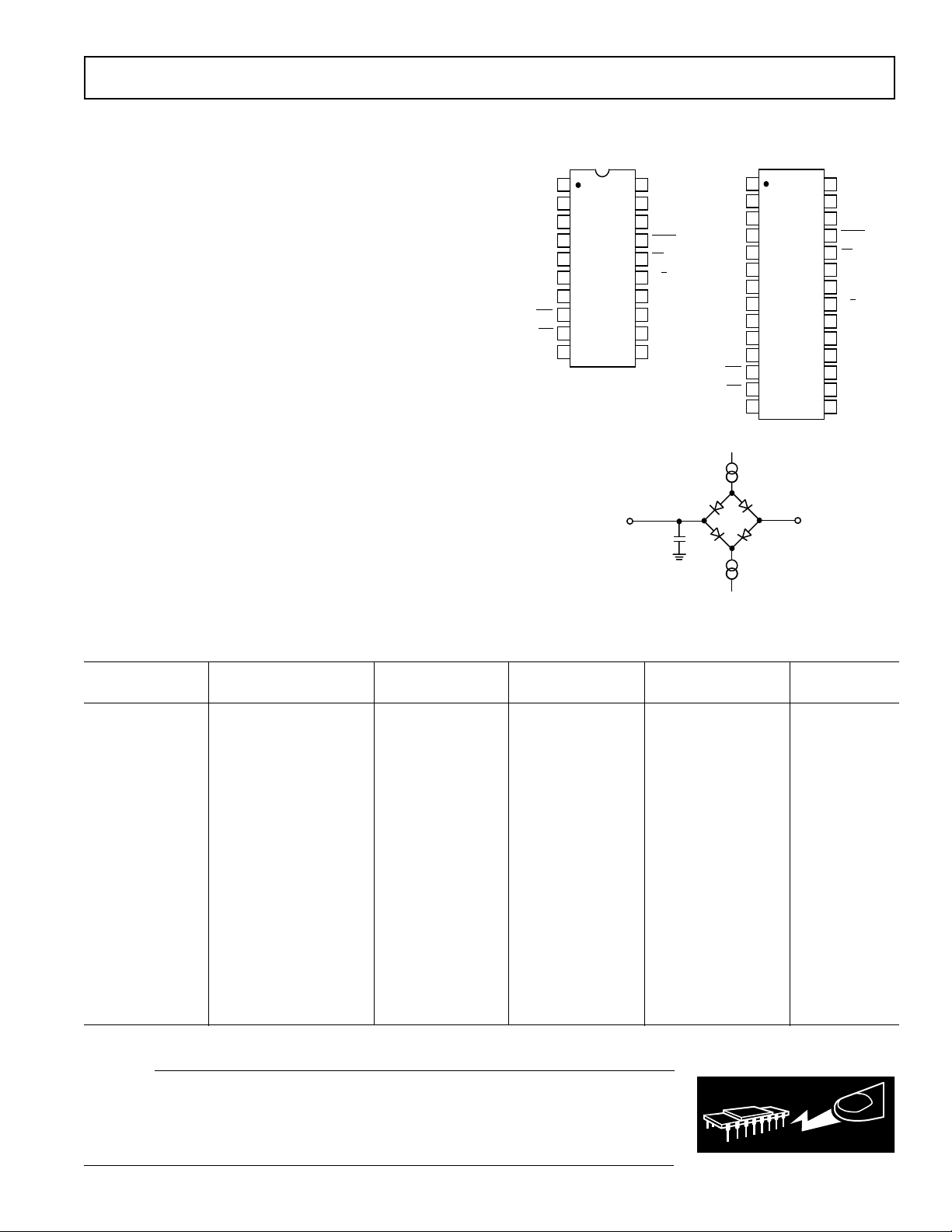
PIN CONFIGURATIONS
SOIC and DIP SSOP
TO OUTPUT
PIN
100pF
C
L
1.6mA I
500AI
OL
1.4V
OH
Figure 1. Load Circuit for Digital Interface Timing
ORDERING GUIDE
Temperature Throughput Package
Model Range Rate Max INL Min S/(N+D) Options*
AD977AN –40°C to +85°C 100 kSPS ± 3.0 LSB 83 dB N-20
AD977BN –40°C to +85°C 100 kSPS ± 2.0 LSB 85 dB N-20
AD977CN –40°C to +85°C 100 kSPS 83 dB N-20
AD977AAN –40°C to +85°C 200 kSPS ± 3.0 LSB 83 dB N-20
AD977ABN –40°C to +85°C 200 kSPS ± 2.0 LSB 85 dB N-20
AD977ACN –40°C to +85°C 200 kSPS 83 dB N-20
AD977AR –40°C to +85°C 100 kSPS ± 3.0 LSB 83 dB R-20
AD977BR –40°C to +85°C 100 kSPS ± 2.0 LSB 85 dB R-20
AD977CR –40°C to +85°C 100 kSPS 83 dB R-20
AD977AAR –40°C to +85°C 200 kSPS ± 3.0 LSB 83 dB R-20
AD977ABR –40°C to +85°C 200 kSPS ± 2.0 LSB 85 dB R-20
AD977ACR –40°C to +85°C 200 kSPS 83 dB R-20
AD977ARS –40°C to +85°C 100 kSPS ± 3.0 LSB 83 dB RS-28
AD977BRS –40°C to +85°C 100 kSPS ± 2.0 LSB 85 dB RS-28
AD977CRS –40°C to +85°C 100 kSPS 83 dB RS-28
AD977AARS –40°C to +85°C 200 kSPS ± 3.0 LSB 83 dB RS-28
AD977ABRS –40°C to +85°C 200 kSPS ± 2.0 LSB 85 dB RS-28
AD977ACRS –40°C to +85°C 200 kSPS 83 dB RS-28
*N = 20-lead 300 mil plastic DIP; R = 20-lead SOIC; RS = 28-lead SSOP.
CAUTION
ESD (electrostatic discharge) sensitive device. Electrostatic charges as high as 4000 V readily
accumulate on the human body and test equipment and can discharge without detection.
Although the AD977/AD977A feature proprietary ESD protection circuitry, permanent damage
may occur on devices subjected to high-energy electrostatic discharges. Therefore, proper ESD
precautions are recommended to avoid performance degradation or loss of functionality.
–5–REV. D

AD977/AD977A
PIN FUNCTION DESCRIPTIONS
Pin No. Pin No.
DIP/SOIC SSOP Mnemonic Description
1, 3, 4 1, 3, 4 R1
, R2IN, R3
IN
Analog Input. Refer to Table I, Table II for input range configuration.
IN
2 2 AGND1 Analog Ground. Used as the ground reference point for the REF pin.
5 6 CAP Reference buffer output. Connect a 2.2 µF tantalum capacitor between CAP and
Analog Ground.
6 7 REF Reference Input/Output. The internal 2.5 V reference is available at this pin.
Alternatively an external reference can be used to override the internal reference. In
either case, connect a 2.2 µF tantalum capacitor between REF and Analog Ground.
7 9 AGND2 Analog Ground.
8 12 SB/BTC This digital input is used to select the data format of a conversion result. With SB/BTC
tied LOW, conversion data will be output in Binary Two’s Complement format. With
SB/BTC connected to a logic HIGH, data is output in Straight Binary format.
9 13 EXT/INT Digital select input for choosing the internal or an external data clock. With EXT/INT
tied LOW, after initiating a conversion, 16 DATACLK pulses transmit the previous
conversion result as shown in Figure 3. With EXT/INT set to a logic HIGH, output
data is synchronized to an external clock signal connected to the DATACLK input.
Data is output as indicated in Figure 4 through Figure 9.
10 14 DGND Digital Ground.
11 15 SYNC Digital output frame synchronization for use with an external data clock
(EXT/INT = Logic HIGH). When a read sequence is initiated, a pulse one
DATACLK period wide is output synchronous to the external data clock.
12 16 DATACLK Serial data clock input or output, dependent upon the logic state of the EXT/INT
pin. When using the internal data clock (EXT/INT = Logic LOW), a conversion
start sequence will initiate transmission of 16 DATACLK periods. Output data is
synchronous to this clock and is valid on both its rising and falling edges (Figure 3).
When using an external data clock (EXT/INT = Logic HIGH), the CS and R/C
signals control how conversion data is accessed.
13 17 DATA The serial data output is synchronized to DATACLK. Conversion results are
stored in an on-chip register. The AD977 provides the conversion result, MSB first,
from its internal shift register. The DATA format is determined by the logic level of
SB/BTC. When using the internal data clock (EXT/INT = Logic LOW), DATA is
valid on both the rising and falling edges of DATACLK. Between conversions
DATA will remain at the level of the TAG input when the conversion was started.
Using an external data clock (EXT/INT = Logic HIGH) allows previous conversion
data to be accessed during a conversion (Figures 5, 7 and 9) or the conversion
result can be accessed after the completion of a conversion (Figures 4, 6 and 8).
14 19 TAG This digital input can be used with an external data clock, (EXT/INT = Logic
HIGH) to daisy chain the conversion results from two or more AD977s onto a
single DATA line. The digital data level on TAG is output on DATA with a delay
of 16 or 17 external DATACLK periods after the initiation of the read sequence.
Dependent on whether a SYNC is not present or present.
15 21 R/C Read/Convert Input. Is used to control the conversion and read modes of the
AD977. With CS LOW; a falling edge on R/C holds the analog input signal inter-
nally and starts a conversion, a rising edge enables the transmission of the conver-
sion result.
16 24 CS Chip Select Input. With R/C LOW, a falling edge on CS will initiate a conversion.
With R/C HIGH, a falling edge on CS will enable the serial data output sequence.
17 25 BUSY Busy Output. Goes LOW when a conversion is started, and remains LOW until the
conversion is completed and the data is latched into the on-chip shift register.
18 26 PWRD Power-Down Input. When set to a logic HIGH power consumption is reduced and
conversions are inhibited. The conversion result from the previous conversion is
stored in the onboard shift register.
19 27 V
20 28 V
ANA
DIG
Analog Power Supply. Nominally 5 V.
Digital Power Supply. Nominally 5 V.
–6–
REV. D

AD977/AD977A
DEFINITION OF SPECIFICATIONS
INTEGRAL NONLINEARITY ERROR (INL)
Linearity error refers to the deviation of each individual code
from a line drawn from “negative full scale” through “positive
full scale.” The point used as “negative full scale” occurs 1/2 LSB
before the first code transition. “Positive full scale” is defined as
a level 1 1/2 LSB beyond the last code transition. The deviation
is measured from the middle of each particular code to the true
straight line.
DIFFERENTIAL NONLINEARITY ERROR (DNL)
In an ideal ADC, code transitions are 1 LSB apart. Differential
nonlinearity is the maximum deviation from this ideal value. It
is often specified in terms of resolution for which no missing
codes are guaranteed.
FULL-SCALE ERROR
The last + transition (from 011 . . . 10 to 011 . . . 11 for two’s
complement format) should occur for an analog voltage 1 1/2 LSB
below the nominal full scale (9.9995422 V for a ±10 V range).
The full-scale error is the deviation of the actual level of the last
transition from the ideal level.
BIPOLAR ZERO ERROR
Bipolar zero error is the difference between the ideal midscale
input voltage (0 V) and the actual voltage producing the
midscale output code.
UNIPOLAR ZERO ERROR
In unipolar mode, the first transition should occur at a level
1/2 LSB above analog ground. Unipolar zero error is the deviation of the actual transition from that point.
SPURIOUS FREE DYNAMIC RANGE
The difference, in decibels (dB), between the rms amplitude of
the input signal and the peak spurious signal.
TOTAL HARMONIC DISTORTION (THD)
THD is the ratio of the rms sum of the first six harmonic components to the rms value of a full-scale input signal and is
expressed in decibels.
SIGNAL TO (NOISE AND DISTORTION) (S/[N+D]) RATIO
S/(N+D) is the ratio of the rms value of the measured input
signal to the rms sum of all other spectral components below the
Nyquist frequency, including harmonics but excluding dc. The
value for S/(N+D) is expressed in decibels.
FULL POWER BANDWIDTH
The full power bandwidth is defined as the full-scale input frequency at which the S/(N+D) degrades to 60 dB, 10 bits of
accuracy.
APERTURE DELAY
Aperture delay is a measure of the acquisition performance, and
is measured from the falling edge of the R/C input to when the
input signal is held for a conversion.
TRANSIENT RESPONSE
The time required for the AD977/AD977A to achieve its rated
accuracy after a full-scale step function is applied to its input.
OVERVOLTAGE RECOVERY
The time required for the ADC to recover to full accuracy after
an analog input signal 150% of full-scale is reduced to 50% of
the full-scale value.
–7–REV. D
AD977/AD977A
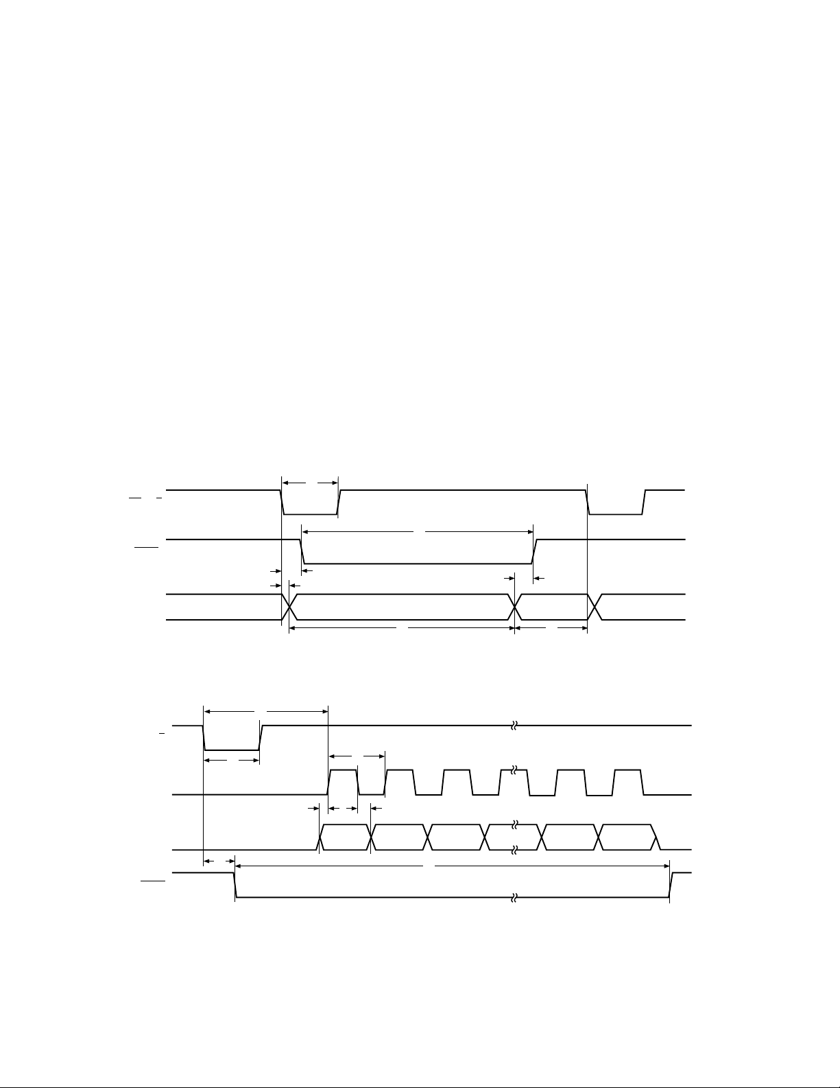
CONVERSION CONTROL
The AD977/AD977A is controlled by two signals: R/C and CS.
When R/C is brought low, with CS low, for a minimum of 50 ns,
the input signal will be held on the internal capacitor array and
a conversion “n” will begin. Once the conversion process does
begin, the BUSY signal will go low until the conversion is complete. Internally, the signals R/C and CS are OR’d together and
there is no requirement on which signal is taken low first when
initiating a conversion. The only requirement is that there be at
least 10 ns of delay between the two signals being taken low.
After the conversion is complete the BUSY signal will return
high and the AD977/AD977A will again resume tracking the
input signal. Under certain conditions the CS pin can be tied
Low and R/C will be used to determine whether you are initiating a conversion or reading data. On the first conversion, after
the AD977/AD977A is powered up, the DATA output will be
indeterminate.
Conversion results can be clocked serially out of the AD977/
AD977A using either an internal clock, generated by the
AD977/AD977A, or by using an external clock. The AD977/
AD977A is configured for the internal data clock mode by pulling the EXT/INT pin low. It is configured for the external clock
mode by pulling the EXT/INT pin high.
t
1
CS, R/C
INTERNAL DATA CLOCK MODE
The AD977/AD977A is configured to generate and provide the
data clock when the EXT/INT pin is held low. Typically CS will
be tied low and R/C will be used to initiate a conversion “n.”
During the conversion the AD977/AD977A will output 16 bits of
data, MSB first, from conversion “n-1” on the DATA pin. This
data will be synchronized with 16 clock pulses provided on the
DATACLK pin. The output data will be valid on both the
rising and falling edge of the data clock as shown in Figure 3.
After the LSB has been presented, the DATA pin will assume
whatever state the TAG input was at during the start of conversion, and the DATACLK pin will stay low until another
conversion is initiated.
EXTERNAL DATA CLOCK MODE
The AD977/AD977A is configured to accept an externally supplied data clock when the EXT/INT pin is held high. This mode
of operation provides several methods by which conversion
results can be read from the AD977/AD977A. The output data
from conversion “n-1” can be read during conversion “n,” or the
output data from conversion “n” can be read after the conversion is complete. The external clock can be either a continuous
or discontinuous clock. A discontinuous clock can be either
BUSY
MODE
R/C
DATACLK
DATA
BUSY
t
3
t
2
t
5
t
6
t
4
ACQUIRE CONVERTACQUIRE CONVERT
t
7
Figure 2. Basic Conversion Timing
t
8
t
t
1
t
10
t
2
9
123 1516
t
11
MSB VALID
BIT 14
VALID
BIT 13
VALID
t
6
BIT 1
VALID
LSB VALID
Figure 3. Serial Data Timing for Reading Previous Conversion Results with Internal Clock (CS, EXT/
Logic Low)
–8–
INT
and TAG Set to
REV. D

AD977/AD977A
normally low or normally high when inactive. In the case of the
discontinuous clock, the AD977/AD977A can be configured to
either generate or not generate a SYNC output (with a continuous clock a SYNC output will always be produced).
Each of the methods will be described in the following sections
and are illustrated in Figures 4 through 9. It should be noted
that all timing diagrams assume that the receiving device is
latching data on the rising edge of the external clock. If the
falling edge of DATACLK is used then, in the case of a discontinuous clock, one less clock pulse is required than shown in
Figures 4 through 7 to latch in a 16-bit word. Note that data is
valid on the falling edge of a clock pulse (for t
greater than t18)
13
and the rising edge of the next clock pulse.
The AD977 provides error correction circuitry that can correct
for an improper bit decision made during the first half of the
conversion cycle. Normally the occurrence of an incorrect bit
decision during a conversion cycle is irreversible. This error
occurs as a result of noise during the time of the decision or due
to insufficient settling time. As the AD977/AD977A is performing a conversion it is important that transitions not occur on
digital input/output pins or degradation of the conversion result
could occur. This is particularly important during the second
half of the conversion process. For this reason it is recommended
that when an external clock is being provided it be a discontinuous clock that is not toggling during the time that BUSY is low
or, more importantly, that it does not transition during the latter
half of BUSY low.
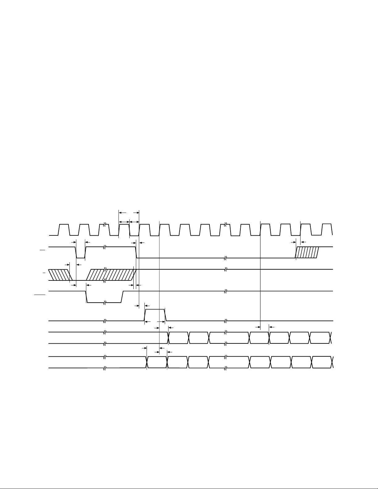
EXTERNAL DISCONTINUOUS CLOCK DATA READ AFTER CONVERSION NO SYNC OUTPUT GENERATED
Figure 4 illustrates the method by which data from conversion
“n” can be read after the conversion is complete using a discontinuous external clock without the generation of a SYNC
output. After a conversion is complete, indicated by BUSY
returning high, the result of that conversion can be read while
CS is Low and R/C is high. In this mode CS can be tied low.
The MSB will be valid on the first falling edge and the second
rising edge of DATACLK. The LSB will be valid on the 16th
falling edge and the 17th rising edge of DATACLK. A minimum of 16 clock pulses are required for DATACLK if the
receiving device will be latching data on the falling edge of
DATACLK. A minimum of 17 clock pulses are required for
DATACLK if the receiving device will be latching data on the
rising edge of DATACLK. Approximately 40 ns after the 17th
rising edge of DATACLK (if provided) the DATA output pin
will reflect the state of the TAG input pin during the first rising
edge of DATACLK.
The advantage of this method of reading data is that it is not
being clocked out during a conversion and therefore conversion
performance is not degraded.
When reading data after the conversion is complete, with the
highest frequency permitted for DATACLK (15.15 MHz), and
with the AD977A, the maximum possible throughput is approximately 195 kHz and not the rated 200 kHz.
For details on use of the TAG input with this mode see the Use
of the Tag Feature section.
t
12
t
t
13
14
EXT
DATACLK
R/C
BUSY
SYNC
DATA
TAG
0 3 14 15 16
t
1
t
2
t
21
t
18
t
t
24
23
TAG 0
12
BIT 15
(MSB)
TAG 1
BIT 14
TAG 2 TAG 3
BIT 13
Figure 4. Conversion and Read Timing Using an External Discontinuous Data Clock (EXT/
to Logic Low)
t
18
BIT 1
TAG 15 TAG 16 TAG 17
BIT 0
(LSB)
INT
Set to Logic High, CS Set
TAG 0
TAG 1
TAG 18
–9–REV. D

AD977/AD977A
EXTERNAL DISCONTINUOUS CLOCK DATA READ DURING CONVERSION NO SYNC OUTPUT GENERATED
Figure 5 illustrates the method by which data from conversion
“n-1” can be read during conversion “n” while using a discontinuous external clock, without the generation of a SYNC output. After a conversion is initiated, indicated by BUSY going
low, the result of the previous conversion can be read while CS
is low and R/C is high. In this mode CS can be tied low. The
MSB will be valid on the 1st falling edge and the 2nd rising
edge of DATACLK. The LSB will be valid on the 16th falling
edge and the 17th rising edge of DATACLK. A minimum of 16
clock pulses are required for DATACLK if the receiving device
will be latching data on the falling edge of DATACLK. A minimum of 17 clock pulses are required for DATACLK if the
receiving device will be latching data on the rising edge of
DATACLK. Approximately 40 ns after the 17th rising edge of
DATACLK (if provided) the DATA output pin will reflect the
state of the TAG input pin during the first rising edge of
DATACLK.
For both the AD977 and the AD977A the data should be
clocked out during the first half of BUSY so not to degrade
conversion performance. For the AD977 this requires use of a
4.8 MHz DATACLK or greater with data being read out as
soon as the conversion process begins. For the AD977A it
requires use of a 10 MHz DATACLK or greater.
It is not recommended that data be shifted through the TAG
input in this mode as it will certainly result in clocking of data
during the second half of the conversion.
EXTERNAL DISCONTINUOUS CLOCK DATA READ
AFTER CONVERSION WITH SYNC OUTPUT GENERATED
Figure 6 illustrates the method by which data from conversion
“n” can be read after the conversion is complete using a discontinuous external clock, with the generation of a SYNC output.
What permits the generation of a SYNC output is a transition of
DATACLK while either CS is high or while both CS and R/C
are low. After a conversion is complete, indicated by BUSY
returning high, the result of that conversion can be read while
CS is Low and R/C is high. In this mode CS can be tied low. In
Figure 6 clock pulse #0 is used to enable the generation of a
SYNC pulse. The SYNC pulse is actually clocked out approximately 40 ns after the rising edge of clock pulse #1. The SYNC
pulse will be valid on the falling edge of clock pulse #1 and the
rising edge of clock pulse #2. The MSB will be valid on the
falling edge of clock pulse #2 and the rising edge of clock pulse
#3. The LSB will be valid on the falling edge of clock pulse #17
and the rising edge of clock pulse #18. Approximately 40 ns
after the rising edge of clock pulse #18 the DATA output pin
will reflect the state of the TAG input pin during the rising edge
of clock pulse #2. The advantage of this method of reading data
is that it is not being clocked out during a conversion and therefore conversion performance is not degraded.
When reading data after the conversion is complete, with the
highest frequency permitted for DATACLK (15.15 MHz),
and with the AD977A, the maximum possible throughput is
approximately 195 kHz and not the rated 200 kHz.
For details on use of the TAG input with this mode see the Use
of the TAG Input section.
t
12
t
t
13
14
EXT
DATACLK
R/C
BUSY
SYNC
DATA
01516
t
15
t
1
t
2
t
21
t
18
12
t
20
BIT 15
(MSB)
BIT 14
t
22
t
18
BIT 0
(LSB)
Figure 5. Conversion and Read Timing for Reading Previous Conversion Results During A Conversion Using External
INT
Discontinuous Data Clock (EXT/
Set to Logic High, CS Set to Logic Low)
–10–
REV. D

AD977/AD977A
BUSY
R/C
EXT
DATACLK
t
13
BIT 15
(MSB)
BIT 14
12
DATA
SYNC
t
14
t
12
0 3 17 18
t
2
t
17
BIT 0
(LSB)
TAG 0 TAG 1
TAG 0 TAG 1 TAG 2
TAG 16 TAG 17 TAG 18
t
18
TAG 19
TAG
TAG 2
4
t
15
t
15
t
15
t
12
t
18
t
24
t
23
Figure 6. Conversion and Read Timing Using An External Discontinuous Data Clock (EXT/
INT
Set to Logic High, CS Set
to Logic Low)
EXTERNAL DISCONTINUOUS CLOCK DATA READ DURING CONVERSION WITH SYNC OUTPUT GENERATED
Figure 7 illustrates the method by which data from conversion
“n-1” can be read during conversion “n” while using a discontinuous external clock, with the generation of a SYNC output.
What permits the generation of a SYNC output is a transition of
DATACLK while either CS is High or while both CS and R/C
are low. In Figure 7 a conversion is initiated by taking R/C low
with CS tied low. While this condition exists a transition of
DATACLK, clock pulse #0, will enable the generation of a
SYNC pulse. Less then 83 ns after R/C is taken low the BUSY
output will go low to indicate that the conversion process has
t
12
t
t
13
14
EXT
DATACLK
t
15
R/C
BUSY
SYNC
DATA
Figure 7. Conversion and Read Timing for Reading Previous Conversion Results During a Conversion Using External
Discontinuous Data Clock (EXT/
0
t
1
t
2
12
t
15
t
17
t
12
t
18
BIT 15
(MSB)
INT
Set to Logic High, CS Set to Logic Low)
began. Figure 7 shows R/C then going high and after a delay of
greater than 15 ns (t
) clock pulse #1 can be taken high to
15
request the SYNC output. The SYNC output will appear
approximately 40 ns after this rising edge and will be valid on
the falling edge of clock pulse #1 and the rising edge of clock
pulse #2. The MSB will be valid approximately 40 ns after the
rising edge of clock pulse #2 and can be latched off either the
falling edge of clock pulse #2 or the rising edge of clock pulse
#3. The LSB will be valid on the falling edge of clock pulse #17
and the rising edge of clock pulse #18. Approximately 40 ns
after the rising edge of clock pulse #18, the DATA output
pin will reflect the state of the TAG input pin during the
rising edge of clock pulse #2.
318
t
22
t
20
t
18
BIT 14
–11–REV. D
BIT 0
(LSB)
TAG 0
AD977/AD977A
For both the AD977 and the AD977A the data should be
clocked out during the first half of BUSY so not to degrade
conversion performance. For the AD977 this requires use of a
4.8 MHz DATACLK or greater, with data being read out as
soon as the conversion process begins. For the AD977A it
requires use of a 10 MHz DATACLK or greater.
It is not recommended that data be shifted through the TAG
input in this mode as it will certainly result in clocking of data
during the second half of the conversion.
EXTERNAL CONTINUOUS CLOCK DATA READ AFTER CONVERSION WITH SYNC OUTPUT GENERATED
Figure 8 illustrates the method by which data from conversion
“n” can be read after the conversion is complete using a continuous external clock, with the generation of a SYNC output.
What permits the generation of a SYNC output is a transition of
DATACLK while either CS is high or while both CS and R/C are
low.
With a continuous clock the CS pin cannot be tied low as it
could be with a discontinuous clock. Use of a continuous clock,
while a conversion is occurring, can increase the DNL and
Transition Noise of the AD977/AD977A.
t
12
t
t
13
14
EXT
DATACLK
CS
t
1
0
1 2 3 4 17 18
t
15
After a conversion is complete, indicated by BUSY returning
high, the result of that conversion can be read while CS is low
and R/C is high. In Figure 8 clock pulse #0 is used to enable the
generation of a SYNC pulse. The SYNC pulse is actually clocked
out approximately 40 ns after the rising edge of clock pulse #1.
The SYNC pulse will be valid on the falling edge of clock pulse
#1 and the rising edge of clock pulse #2. The MSB will be valid
on the falling edge of clock pulse #2 and the rising edge of clock
pulse #3. The LSB will be valid on the falling edge of clock
pulse #17 and the rising edge of clock pulse #18. Approximately
50 ns after the rising edge of clock pulse #18 the DATA output
pin will reflect the state of the TAG input pin during the rising
edge of clock pulse #2.
When reading data after the conversion is complete, with the
highest frequency permitted for DATACLK (15.15 MHz) and,
with the AD977A, the maximum possible throughput is approximately 195 kHz and not the rated 200 kHz.
For details on use of the TAG input with this mode see the Use
of the TAG Input section.
t
19
t
16
R/C
t
16
t
17
t
12
t
18
BIT 15
(MSB)
t
23
t
24
TAG 0 TAG 1
BIT 14
TAG 2
TAG 16 TAG 17 TAG 18 TAG 19
BUSY
SYNC
DATA
TAG
t
2
Figure 8. Conversion and Read Timing Using an External Continuous Data Clock (EXT/
BIT 0
(LSB)
t
18
TAG 0 TAG 1 TAG 2
INT
Set to Logic High)
–12–
REV. D

AD977/AD977A
CS
BUSY
R/C
EXT
DATACLK
BIT 15
(MSB)
1
DATA
SYNC
03
BIT 0
(LSB)
TAG 0 TAG 1
TAG 0
TAG
2
t
13
t
14
t
12
t
19
18
t
15
t
16
t
1
t
20
t
2
t
17
t
12
t
18
t
23
t
24
t
18
TAG 2
TAG 1 TAG 16 TAG 17 TAG 18 TAG 19
EXTERNAL CONTINUOUS CLOCK DATA READ DURING CONVERSION WITH SYNC OUTPUT GENERATED
Figure 9 illustrates the method by which data from conversion
“n-1” can be read during conversion “n” while using a continuous external clock with the generation of a SYNC output. What
permits the generation of a SYNC output is a transition of
DATACLK while either CS is high or while both CS and R/C
are low.
With a continuous clock the CS pin cannot be tied low as it
could be with a discontinuous clock. Use of a continuous clock
while a conversion is occurring can increase the DNL and
Transition Noise of the AD977/AD977A.
In Figure 9 a conversion is initiated by taking R/C low with CS
held low. While this condition exists a transition of DATACLK,
clock pulse #0, will enable the generation of a SYNC pulse.
Less then 83 ns after R/C is taken low the BUSY output will go
low to indicate that the conversion process has began. Figure 9
shows R/C then going high and after a delay of greater than
15 ns (t
), clock pulse #1 can be taken high to request the
15
SYNC output. The SYNC output will appear approximately
50 ns after this rising edge and will be valid on the falling edge
of clock pulse #1 and the rising edge of clock pulse #2. The
MSB will be valid approximately 40 ns after the rising edge of
clock pulse #2 and can be latched off either the falling edge of
clock pulse #2 or the rising edge of clock pulse #3. The LSB
will be valid on the falling edge of clock pulse #17 and the rising
edge of clock pulse #18. Approximately 40 ns after the rising
edge of clock pulse #18, the DATA output pin will reflect the
state of the TAG input pin during the rising edge of clock
pulse #2.
For both the AD977 and the AD977A the data should be
clocked out during the 1st half of BUSY so as not to degrade
conversion performance. For the AD977 this requires use of a
4.8 MHz DATACLK or greater with data being read out as
soon as the conversion process begins. For the AD977A it
requires use of a 10 MHz DATACLK or greater.
Figure 9. Conversion and Read Timing for Reading Previous Conversion Results During a Conversion Using An External
INT
Continuous Data Clock (EXT/
Set to Logic High)
–13–REV. D

AD977/AD977A
Table I. AD977A Analog Input Configuration
Input Voltage Connect R1
IN
Connect R2
IN
Connect R3
IN
Input
Range via 200 to via 100 to to Impedance
± 10 V V
IN
± 5 V AGND V
± 3.3 V V
IN
0 V to 10 V AGND V
0 V to 5 V AGND AGND V
0 V to 4 V V
IN
AGND 2.5 V 11.5 kΩ
IN
V
IN
IN
AGND V
2.5 V 6.7 kΩ
2.5 V 5.4 kΩ
AGND 6.7 kΩ
IN
IN
5.0 kΩ
5.4 kΩ
Table II. AD977 Analog Input Configuration
Input Voltage Connect R1
IN
Connect R2
IN
Connect R3
IN
Input
Range via 200 to via 100 to to Impedance
± 10 V V
IN
± 5 V AGND V
± 3.3 V V
IN
0 V to 10 V AGND V
0 V to 5 V AGND AGND V
0 V to 4 V V
IN
ANALOG INPUTS
The AD977/AD977A is specified to operate with six full-scale
analog input ranges. Connections required for each of the three
analog inputs, R1
, R2IN and R3IN, and the resulting full-scale
IN
ranges, are shown in Table I and Table II. The nominal input
impedance for each analog input range is also shown. Table III
shows the output codes for the ideal input voltages of each of the
six analog input ranges.
The analog input section has a ±25 V overvoltage protection on
R1
and R2IN. Since the AD977/AD977A has two analog
IN
grounds it is important to ensure that the analog input is referenced to the AGND1 pin, the low current ground. This will
minimize any problems associated with a resistive ground drop.
It is also important to ensure that the analog input of the
AD977/AD977A is driven by a low impedance source. With its
primarily resistive analog input circuitry, the ADC can be driven
by a wide selection of general purpose amplifiers.
To best match the low distortion requirements of the AD977/
AD977A, care should be taken in the selection of the drive circuitry op amp.
Figure 10 shows the simplified analog input section for the
AD977/AD977A. Since the AD977/AD977A can operate with
an internal or external reference, and several different analog
input ranges, the full-scale analog input range is best represented
with a voltage that spans 0 V to V
across the 40 pF sampling
REF
capacitor. The onboard resistors are laser trimmed to ratio
match for adjustment of offset and full-scale error using fixed
external resistors.
AGND CAP 22.9 kΩ
IN
V
IN
IN
AGND V
CAP 13.3 kΩ
CAP 10.7 kΩ
AGND 13.3 kΩ
IN
IN
10.0 kΩ
10.7 kΩ
that a single 5 V supply can be used to bias the hardware trim
circuitry. With the hardware adjust circuits shown in Figures 12
and 13, offset and full-scale error can be trimmed to zero. Refer
to the Offset and Gain Adjust section.
If larger offset and full-scale errors are permitted, or if software calibration is used, the external resistors can be omitted. Table IV shows the resultant input ranges and offset and
full-scale errors.
Using the AD977A with Bipolar Input Ranges
The connection diagrams in Figure 11 show a buffer amplifier
required for bipolar operation of the AD977A when using the
internal reference. The buffer amplifier is required to isolate the
CAP pin from the signal dependent current in the R3
pin. A
IN
high speed op amp such as the AD8031 can be used with a
single 5 V power supply without degrading the performance of
the AD977A. The buffer must have good settling characteristics
and provide low total noise within the input bandwidth of the
AD977A.
REF
20k /10k
4k
2.5V
REFERENCE
SWITCHED
CAP ADC
40pF
CAP
R1
R2
R3
AGND2
20k /10k
IN
10k /5k
IN
5k /2.5k
IN
AD977/AD977A
AGND1
The configurations shown in Figures 12 and 13 are required to
obtain the data sheet specifications for offset and full-scale error.
The external fixed resistors are used during factory calibration so
Figure 10. AD977/AD977A Simplified Analog Input
–14–
REV. D

AD977/AD977A
Table III. Output Codes and Ideal Input Voltages
Digital Output
Description Analog Input (SB/BTC LOW) (SB/BTC HIGH)
Full-Scale Range ±10 V ± 5 V ±3.33 V 0 V to 10 V 0 V to 5 V 0 V to 4 V
Least Significant Bit 305 µV 153 µV 102 µV 153 µV 76 µV 61 µV
+Full Scale (FS–1 LSB) 9.999695 V 4.999847 V 3.333231 V 9.999847 V 4.999924 V 3.999939 V 0111 1111 1111 1111 1111 1111 1111 1111
Midscale 0 V 0 V 0 V 5 V 2.5 V 2 V 0000 0000 0000 0000 1000 0000 0000 0000
One LSB Below Midscale –305 µV –153 µV –102 µV 4.999847 V 2.499924 V 1.999939 V 1111 1111 1111 1111 0111 1111 1111 1111
–Full Scale –10 V –5 V –3.333333 V 0 V 0 V 0 V 1000 0000 0000 0000 0000 0000 0000 0000
Table IV. Input Ranges, Offset and Full-Scale Errors Without External Resistors
AD977 Offset Error Full-Scale Error AD977A Offset Error Full-Scale Error
Input Range A/B/C Grade A/B/C Grade Input Range A/B/C Grade A/B/C Grade
–9.890 V to 9.90 V ±25 mV/± 25 mV ±0.75%/±0.50% –9.800 V to 9.970 V ±40 mV/±40 mV ± 0.80%/± 0.55%
–4.943 V to 4.995 V ±25 mV/± 25 mV ± 0.75%/± 0.50% –4.900 V to 4.985 V ± 40 mV/± 40 mV ± 0.80%/±0.55%
–3.295 V to 3.330 V ±25 mV/± 25 mV ± 0.75%/± 0.50% –3.267 V to 3.323 V ± 40 mV/± 40 mV ± 0.80%/±0.55%
0.008 V to 9.946 V ± 10 mV/± 10 mV ± 0.75%/± 0.50% 0.007 V to 9.893 V ± 10 mV/± 10 mV ±0.75%/± 0.50%
0.004 V to 5.023 V ± 10 mV/± 10 mV ± 0.75%/± 0.50% 0.004 V to 5.039 V ± 10 mV/± 10 mV ±0.75%/± 0.50%
0.003 V to 4.010 V ± 10 mV/± 10 mV ± 0.75%/± 0.50% 0.003 V to 4.016 V ± 10 mV/± 10 mV ±0.75%/± 0.50%
Two’s Complement Straight Binary
V
IN
100
33.2k
2.2 F
200
2.2
AD8031
F
a.
R1
IN
AGND1
R2
IN
R3
IN
CAP
AD977A
REF
AGND2
V
200
IN
33.2k
100
2.2 F
2.2
AD8031
F
b.
R1
IN
AGND1
R2
IN
R3
IN
CAP
AD977A
REF
AGND2
V
IN
100
33.2k
AD8031
2.2
200
2.2 F
R1
IN
AGND1
R2
IN
R3
IN
CAP
AD977A
REF
F
AGND2
c.
Figure 11. AD977A Bipolar Input Configuration Using the Internal Reference; (a) VIN = ±10 V, (b) VIN = ±5 V, (c) VIN = ±3.33 V
–15–REV. D

AD977/AD977A
BIPOLAR CONNECTION FOR AD977
INPUT
RANGE
10V
5V
STANDARD CONNECTION WITHOUT
OFFSET AND GAIN ADJUST
100
33.2k
2.2F
200
100
33.2k
2.2F
200
2.2F
2.2F
R1
IN
AGND1
R2
IN
R3
IN
CAP
AD977
REF
AGND2
R1
IN
AGND1
R2
IN
R3
IN
CAP
AD977
REF
AGND2
V
IN
V
IN
STANDARD CONNECTION WITH
OFFSET AND GAIN ADJUST
5V
100
5V
33.2k
200
200
100
576k
2.2F
576k
2.2F
2.2F
2.2F
R1
IN
AGND1
R2
IN
R3
IN
CAP
AD977
REF
AGND2
R1
IN
AGND1
R2
IN
R3
IN
CAP
AD977
REF
AGND2
50k
50k
V
IN
5V
33.2k
50k
5V
V
IN
50k
3.33V
V
IN
100
33.2k
2.2F
200
2.2F
R1
IN
AGND1
R2
IN
R3
IN
CAP
AD977
REF
AGND2
50k
V
IN
100
5V
33.2k
5V
50k
Figure 12. AD977 Bipolar Analog Input Configuration
200
2.2F
576k
2.2F
R1
IN
AGND1
R2
IN
R3
IN
CAP
AD977
REF
AGND2
–16–
REV. D

UNIPOLAR CONNECTION FOR AD977A AND AD977
AD977/AD977A
INPUT
RANGE
0V–10V
0V–5V
STANDARD CONNECTION WITHOUT
OFFSET AND GAIN ADJUST
200
100
V
IN
33.2k
2.2F
2.2F
200
33.2k
V
IN
2.2F
2.2F
100
R1
IN
AGND1
R2
IN
R3
IN
CAP
AD977/
AD977A
REF
AGND2
R1
IN
AGND1
R2
IN
R3
IN
CAP
AD977/
AD977A
REF
AGND2
STANDARD CONNECTION WITH
OFFSET AND GAIN ADJUST
V
2.2F
V
IN
50k
50k
IN
200
100
5V
33.2k
5V
50k
5V
+
–
50k
576k
2.2F
200
33.2k
5V
576k
2.2F
2.2F
100
R1
IN
AGND1
R2
IN
R3
IN
CAP
AD977/
AD977A
REF
AGND2
R1
IN
AGND1
R2
IN
R3
IN
CAP
AD977/
AD977A
REF
AGND2
0V–4V
200
2.2F
5V
576k
2.2F
2.2F
200
100
33.2k
2.2F
R1
IN
AGND1
R2
IN
R3
IN
CAP
AD977/
AD977A
REF
AGND2
V
IN
50k
V
IN
100
5V
33.2k
50k
Figure 13. AD977/AD977A Unipolar Analog Input Configuration
R1
IN
AGND1
R2
IN
R3
IN
CAP
AD977/
AD977A
REF
AGND2
–17–REV. D

AD977/AD977A
VOLTAGE REFERENCE
The AD977/AD977A has an on-chip temperature compensated
bandgap voltage reference that is factory trimmed to 2.5 V
± 20 mV. The accuracy of the AD977/AD977A over the specified temperature ranges is dominated by the drift performance
of the voltage reference. The on-chip voltage reference is lasertrimmed to provide a typical drift of 7 ppm/°C. This typical drift
characteristic is shown in Figure 14, which is a plot of the
change in reference voltage (in mV) versus the change in temperature—notice the plot is normalized for zero error at 25°C.
If improved drift performance is required, an external reference
such as the AD780 should be used to provide a drift as low as
3 ppm/°C. In order to simplify the drive requirements of the
voltage reference (internal or external), an onboard reference
buffer is provided. The output of this buffer is provided at the
CAP pin and is available to the user; however, when externally
loading the reference buffer, it is important to make sure that
proper precautions are taken to minimize any degradation in the
ADC’s performance. Figure 15 shows the load regulation of the
reference buffer. Notice that this figure is also normalized so
that there is zero error with no dc load. In the linear region, the
output impedance at this point is typically 1 Ω. Because of this
1 Ω output impedance, it is important to minimize any ac or
1mV/DIV
–55
25 125
DEGREES CELSIUS
input dependent loads that will lead to increased distortion.
Any dc loads will simply act as a gain error. Although the typical characteristic of Figure 15 shows that the AD977/AD977A
is capable of driving loads greater than 15 mA, it is recommended that the steady state current not exceed 2 mA.
Using an External Reference
In addition to the on-chip reference, an external 2.5 V reference can be applied. When choosing an external reference for a
16-bit application, however, careful attention should be paid to
noise and temperature drift. These critical specifications can
have a significant effect on the ADC performance.
Figures 16a and 16b show the AD977/AD977A used in bipolar
mode with the AD780 voltage reference applied to the REF
pin. It is important to note that in Figure 16a the R3
connected to the CAP pin whereas in Figure 16b the R3
pin is
IN
IN
pin
of the AD977A is returned to the output of the external reference. The AD780 is a bandgap reference that exhibits ultralow
drift, low initial error and low output noise. In Figure 16b,
the value for C1 is only applicable to applications using the
AD780. In applications using a different external reference a
different value for C1 may be required. For low power applications, the REF192 provides a low quiescent current, high
accuracy and low temperature drift solution.
V
OUT
GND
200
6
4
100
C3
1F
C1
2.2F
33.2k
C4
0.1F
C2
2.2F
R1
IN
R2
IN
R3
IN
REF
AGND1
AD977
V
ANA
CAP
AGND2
V
IN
0.1F
3
TEMP
AD780
2
5V
V
IN
Figure 14. Reference Drift
dV ON CAP PIN – 10mV/DIV
SOURCE CAPABILITY SINK CAPABILITY
LOAD CURRENT – 5mA/DIV
Figure 15. CAP Pin Load Regulation
Figure 16a. AD780 External Reference to AD977 Configured for
±
10 V Input Range
V
0.1F
3
TEMP
AD780
2
5V
*ESR AT 100kHz MUST BE LESS THAN 0.3.
RECOMMEND KEMET T495 SERIES OR
SANYO 6SA330M.
V
IN
200
IN
V
OUT
GND
100
6
4
C3
1F
33.2k
C1
330F*
C4
0.1F
2.2F
R1
IN
R2
IN
R3
IN
REF
AGND1
AD977A
V
ANA
CAP
C2
AGND2
Figure 16b. AD780 External Reference to AD977A Config-
±
ured for
10 V Input Range
–18–
REV. D

AD977/AD977A
OFFSET AND GAIN ADJUSTMENT
The AD977/AD977A is factory trimmed to minimize gain,
offset and linearity errors. In some applications, where the analog input signal is required to meet the full dynamic range of the
ADC, the gain and offset errors need to be externally trimmed
to zero. Figures 12 and 13 show the required trim circuitry to
correct for these offset and gain errors.
Where adjustment is required, offset error must be corrected
before gain error. To achieve this in the bipolar input configuration, trim the offset potentiometer with the input voltage set to
1/2 LSB below ground. Then adjust the potentiometer until the
major carry transition is located between 1111 1111 1111 1111
and 0000 0000 0000 0000. To adjust the gain error, an analog
signal should be input at either the first code transition (ADC
negative full scale) or the last code transition (ADC positive full
scale). Thus, to adjust for full-scale error, an input voltage of
FS/2 – 3/2 LSBs can be applied to V
, and the gain potentiom-
IN
eter should be adjusted until the output code flickers between
the last positive code transition 0111 1111 1111 1111 and 0111
1111 1111 1110. Should the first code transition need adjusting, the trim procedure should consist of applying an analog
input signal of –FS/2 + 1/2 LSB to the V
input and adjust-
IN
ing the trim until the output code flickers between 1000 0000
0000 0000 and 1000 0000 0000 0001.
AC PERFORMANCE
The AD977/AD977A is fully specified and tested for dynamic
performance specifications. The ac parameters are required for
signal processing applications such as speech recognition and
spectrum analysis. These applications require information on
the ADC’s effect on the spectral content of the input signal.
Hence, the parameters for which the AD977/AD977A is specified
include S/(N+D), THD and Spurious Free Dynamic Range.
These terms are discussed in greater detail in the following
sections.
As a general rule, it is recommended that the results from several conversions be averaged to reduce the effects of noise and
thus improve parameters such as S/(N+D) and THD. The ac
performance of the AD977/AD977A can be optimized by operating the ADC at its maximum sampling rate of 100 kHz/200 kHz
and digitally filtering the resulting bit stream to the desired signal
bandwidth. By distributing noise over a wider frequency range
the noise density in the frequency band of interest can be
reduced. For example, if the required input bandwidth is 50 kHz,
0
–10
–20
–30
–40
–50
–60
–70
–80
AMPLITUDE – dB
–90
–100
–110
–120
–130
0 10010 20 30 40
FREQUENCY – kHz
5280 POINT FFT
= 200kHz
F
SAMPLE
= 20kHz, 0dB
F
IN
SNRD = 86dB
THD = –101dB
50 60 70 80 90 955 1525354555657585
Figure 17. FFT Plot
–19–REV. D
the AD977/AD977A could be oversampled by a factor of 2/4.
This would yield a 3/6 dB improvement in the effective SNR
performance.
DC PERFORMANCE
The factory calibration scheme used for the AD977/AD977A
compensates for bit weight errors that may exist in the capacitor
array. The mismatch in capacitor values is adjusted (using the
calibration coefficients) during a conversion resulting in excellent dc linearity performance. Figures 18, 19, 20, 21, 22 and 23,
respectively, show typical INL, typical DNL, typical positive and
negative INL and DNL distribution plots for the AD977/AD977A
at 25°C.
A histogram test is a statistical method for deriving an A/D
converter’s differential nonlinearity. A ramp input is sampled by
the ADC and a large number of conversions are taken at each
voltage level, averaged then stored. The effect of averaging is to
reduce the transition noise by 1/n. If 64 samples are averaged at
each point, the effect of transition noise is reduced by a factor of
8, i.e., a transition noise of 0.8 LSBs rms is reduced to
0.1 LSBs rms. Theoretically the codes, during a test of DNL,
would all be the same size and therefore have an equal number
of occurrences. A code with an average number of occurrences
would have a DNL of “0.” A code that is different from the
average would have a DNL that was either greater or less than
zero LSB. A DNL of –1 LSB indicates that there is a missing
code present at the 16-bit level and that the ADC exhibits 15bit performance.
2.0
1.5
1.0
0.5
0
LSB
–0.5
–1.0
–1.5
–2.0
0665 1015 20253035
100%
40 45 50 55 60
OUTPUT CODE – K
Figure 18. INL Plot
2.0
1.5
1.0
0.5
0
LSB
–0.5
–1.0
–1.5
–2.0
0665 101520253035
100%
40 45 50 55 60
OUTPUT CODE – K
Figure 19. DNL Plot

AD977/AD977A
50
45
40
35
30
25
20
NUMBER OF UNITS
15
10
5
0
0
0.2
0.3
0.4
0.5
0.6
0.8
0.911.1
1.2
1.4
1.5
1.6
1.7
POSITIVE INL – LSB
1.822.1
2.2
2.3
2.4
2.6
2.7
2.8
2.9
Figure 20. Typical Positive INL Distribution (999 Units)
60
50
40
30
20
NUMBER OF UNITS
10
0
–2.5
–2.4
–2.3
–2.2
–2.1
–2.0
–1.9
–1.8
–1.7
–1.6
NEGATIVE INL – LSB
–1.5
–1.4
–1.3
–1.2
–1.1
–1.0
–0.9
–0.8
–0.7
–0.6
–0.5
–0.4
–0.3
–0.2
–0.1
Figure 21. Typical Negative INL Distribution (999 Units)
90
80
70
60
50
40
30
NUMBER OF UNITS
20
10
0
–0.97
–1.02
–1.07
–1.22
–1.17
–1.12
–0.87
–0.82
–0.78
–0.73
–0.68
–0.92
–0.63
NEGATIVE DNL – LSB
–0.58
–0.53
–0.48
–0.43
–0.38
–0.33
–0.28
–0.23
–0.18
–0.14
–0.09
–0.04
Figure 23. Typical Negative DNL Distribution (999 Units)
90
80
70
= 0dB
60
IN
50
40
30
SINAD (dB) FOR V
20
10
1 10 100 1000
INPUT SIGNAL FREQUENCY – kHz
SNR+D (dB) FOR AD977A
SNR+D (dB) FOR AD977
Figure 24. S/(N+D) vs. Input Frequency
120
100
80
60
40
NUMBER OF UNITS
20
0
0.02
0.10
0.19
0.27
0.36
0.44
0.52
0.61
0.69
0.77
0.86
0.94
1.02
1.11
1.19
1.27
1.36
1.44
1.53
1.61
1.69
1.78
1.86
1.94
POSITIVE DNL – LSB
2.03
Figure 22. Typical Positive DNL Distribution (999 Units)
110
105
100
95
90
SFDR, S/N+D – dB
85
80
–75 150–50
–25 0 25 50 75 100 125
SFDR
THD
SNRD
TEMPERATURE – C
Figure 25. AC Parameters vs. Temperature
–80
–85
–90
–95
THD – dB
–100
–105
–110
–20–
REV. D

AD977/AD977A
DC CODE UNCERTAINTY
Ideally, a fixed dc input should result in the same output code
for repetitive conversions; however, as a consequence of unavoidable circuit noise within the wideband circuits of the ADC, a
range of output codes may occur for a given input voltage.
Thus, when a dc signal is applied to the AD977/AD977A input
and 10,000 conversions are recorded, the result will be a distribution of codes as shown in Figure 26. This histogram shows a
bell shaped curve consistent with the Gaussian nature of thermal
noise. The histogram is approximately seven codes wide. The
standard deviation of this Gaussian distribution results in a code
transition noise of 1 LSB rms.
4000
3500
3000
2500
2000
1500
1000
500
0
–3
–2 –10 1 2 3 4
Figure 26. Histogram of 10,000 Conversions of a DC Input
USE OF THE TAG INPUT
The AD977/AD977A provides a TAG input pin for cascading
multiple converters together. This feature is useful for reducing
component count in systems where an isolation barrier must be
crossed and is also useful for systems with a limited capacity for
interfacing to a large number of converters.
The tag feature only works in the external clock mode and
requires that the DATA output of a “upstream” device be connected to the TAG input of an “downstream” device.
An example of the concatenation of two devices is shown in
Figure 27 and their resultant output is shown in Figure 28.
In Figure 27, the paralleled R/C ensures that each AD977/
AD977A will simultaneously sample their inputs. In Figure 28,
a “null” bit is shown between each 16-bit word associated with
each ADC in the serial data output stream. This is the result of
a minimum value for “External Data Clock to Data Valid Delay”
(t
) that is greater than the “TAG Valid Setup Time” (t23). In
18
other words, when you concatenate two or more AD977/AD977As
the MSB on the downstream device will not be present on the
TAG input of the upstream device in time to meet the setup
time requirement of the TAG input.
If the serial data stream is going to a parallel port of a microprocessor that is also providing the serial data clock, then the
microprocessor’s firmware can be written to “throw away” the
null bit. If the serial data stream is going to a serial port then
external “glue” logic will have to be added to make the interface
work. If the serial port has a “sync” input then this can be used
to throw away the null bit if the sync input is toggled each time
the null bit appears.
If the application does not require simultaneous sampling, the
null bit can be completely avoided by delaying the R/C signal
of each upstream device by one clock cycle with respect to its
immediate downstream device. This bit time delay can be accomplished through a D-type flip-flop that delays the R/C signal at
its D-input by one cycle of the serial data clock that is at its
clock input.
DCLK IN
R/
IN
IN
AD977/AD977A
#2
(UPSTREAM)
TAG DATA
R/C
DCLK
CS
AD977/AD977A
#1
(DOWNSTREAM)
TAG
DATA
DCLK
DATA OUT
CS
R/C
Figure 27. Two AD977/AD977A’s Utilizing Tag
It is not recommended that the TAG feature be used with the
read during convert mode because this will require data to be
clocked out during the second half of the conversion process. It
is recommended that the read after convert mode be used in an
application that wants to take advantage of the TAG feature. To
improve the data throughput a combination of the two data read
methods can be used and is described as follows.
If two or more AD977/AD977As are to have their data output
concatenated together in a single data stream, and if data
throughput is to be maximized, a system could be designed such
that the upstream device data is read during the first half of its
conversion process and the remainder of the downstream devices
read during the time between conversions. Assume three AD977As
are to have their data concatenated. Assume the further most
downstream device is referred to as device #1 and the further
most upstream device as #3. Each device is driven from a common DATACLK and R/C control signal, the CS input of each
device is tied to ground. The three BUSY outputs should be
OR’d together to form a composite BUSY. After the conversion
is complete, as indicated by the composite BUSY going high, an
external, normally low, 15.15 MHz DATACLK can be toggled
34 times to first read the data first from device #3 and then
from device #2. When the composite BUSY goes low to indicate
the beginning of the conversion process the external DATACLK can be toggled 17 times to read the data from device #1
during the first half of the conversion process. Using this technique it would be possible to read in the data from the three
devices in approximately 6.4 µs for a throughput of approxi-
mately 156 kHz The receiving device would have to deal with
the null bit between data from device #2 and #3. The receiving
device would also have to be capable of starting and stopping
the external DATACLK at the appropriate times.
The TAG input, when unused, should always be tied either high
or low and not be allowed to float.
–21–REV. D

AD977/AD977A
R/C
BUSY
DATA
DCLK
15 0
DEVICE DATA #1
NULL BIT
15
DEVICE
DATA #2
Figure 28. TAG Timing Diagram for Two Concatenated
AD977/AD977As
POWER-DOWN FEATURE
The AD977/AD977A has analog and reference power-down
capability through the PWRD pin. When the PWRD pin is
taken high, the power consumption drops from a maximum
value of 100 mW to a typical value of 50 µW. When in the
power-down mode the previous conversion results are still available in the internal registers and can be read out providing it has
not already been shifted out.
When used with an external reference, connected to the REF
pin and a 2.2 µF capacitor, connected to the CAP pin, the
power up recovery time is typically 1 ms. This typical value of
1 ms for recovery time depends on how much charge has decayed
from the external 2.2 µF capacitor on the CAP pin and assumes
that it has decayed to zero. The 1 ms recovery time has been
specified such that settling to 16-bits has been achieved.
When used with the internal reference, the dominant time constant for power-up recovery is determined by the external
capacitor on the REF pin and the internal 4K impedance seen
at that pin. An external 2.2 µF capacitor is recommended for the
REF pin.
CONSIDERATIONS WHEN USING MULTIPLEXED
INPUTS
Consideration must be given to the effect on A/D performance
in applications that require the use of analog multiplexers or analog
switches to interface multiple signals to the AD977/AD977A. The
nonzero “on” resistance of a multiplexer or switch, at the input
to the AD977/AD977A, will increase the system offset and gain
error. As an example, consider the AD977 configured for an input
voltage range of ±10 V dc. For every 5 Ω of source impedance
(in addition to the required external 200 Ω input resistor) an
offset error of 1 LSB would be introduced and the positive
gain error would increase by an added 0.00375% of full scale.
This error, due to nonzero source impedance, can be corrected through a hardware or software system level calibration,
but will only be valid at the temperature and input voltage
present at the time of calibration. Another factor to consider is
that most analog multiplexers and switches exhibit a nonlinear
relationship between input signal level and on resistance. This
will introduce added distortion products that will degrade THD,
S/(N+D) and INL. For these reasons it is recommended that an
appropriate buffer be used between the output of the multiplexer
and the input of the AD977.
When switching the input to the multiplexer, and subsequently
the input to the AD977, it is recommended that the transition
be made to occur either immediately after the current conversion is complete or shortly after the beginning of a conversion.
MICROPROCESSOR INTERFACING
The AD977/AD977A is ideally suited for traditional dc measurement applications supporting a microprocessor, and ac
signal processing applications interfacing to a digital signal
processor. The AD977/AD977A is designed to interface with a
general purpose serial port or I/O ports on a microcontroller. A
variety of external buffers can be used with the AD977/AD977A
to prevent digital noise from coupling into the ADC. The
following sections illustrate the use of the AD977/AD977A with
an SPI equipped microcontroller and the ADSP-2181 signal
processor.
SPI Interface
Figure 29 shows a general interface diagram between the
AD977/AD977A and an SPI equipped microcontroller. This
interface assumes that the convert pulses will originate from the
microcontroller and that the AD977/AD977A will act as the
slave device. The convert pulse could be initiated in response to
an internal timer interrupt. The reading of output data, one byte
at a time, if necessary, could be initiated in response to the endof-conversion signal (BUSY going high).
SDI
SCK
I/O PORT
IRQ
SPI
+5V
DATA
DATACLK
R/C
BUSY
EXT/INT
CS
TAG
AD977/
AD977A
Figure 29. AD977/AD977A to SPI Interface
ADSP-2181 Interface
Figure 30 shows an interface between the AD977/AD977A and
the ADSP-2181 Digital Signal Processor. The AD977/AD977A
is configured for the Internal Clock mode (EXT/INT = 0) and
will therefore act as the master device. The convert command is
shown generated from an external oscillator in order to provide
a low jitter signal appropriate for both dc and ac measurements.
Because the SPORT, within the ADSP-2181, will be seeing a
discontinuous external clock, some steps are required to ensure
that the serial port is properly synchronized to this clock during
each data read operation. The recommended procedure to ensure
this is as follows,
– enable SPORT0 through the System Control register
– set the SCLK Divide register to zero
– setup PF0 and PF1 as outputs by setting bits 0 and 1 in
PFTYPE
– force RFS0 low through PF0. The Receive Frame Sync signal
has been programmed active high
– enable AD977/AD977A by forcing CS = 0 through PF1
– enable SPORT0 Receive Interrupt through the IMASK register
– wait for at least one full conversion cycle of the AD977/AD977A
and throw away the received data
– disable the AD977/AD977A by forcing CS = 1 through PF1
– wait for a period of time equal to one conversion cycle
– force RFS0 high through PF0
– enable the AD977/AD977A by forcing CS = 0 through PF1
–22–
REV. D

AD977/AD977A
The ADSP-2181 SPORT0 will now remain synchronized to the
external discontinuous clock for all subsequent conversions.
DR0
SCLK0
ADSP-2181
RFS0
SPORT0 CNTRL REG = 0x300F
OSCILLATOR
PF1
PF0
DATA
DATACLK
R/C
CS
EXT/INT
TAG
AD977/
AD977A
Figure 30. AD977/AD977A to ADSP-2181 Interface
POWER SUPPLIES AND DECOUPLING
The AD977/AD977A has two power supply input pins. V
and V
portions, respectively. V
analog circuitry, and V
provide the supply voltages to the analog and digital
DIG
is the 5 V supply for the on-chip
ANA
is the 5 V supply for the on-chip
DIG
ANA
digital circuitry. The AD977/AD977A is designed to be independent of power supply sequencing and thus free from supply
voltage induced latchup.
With high performance linear circuits, changes in the power
supplies can result in undesired circuit performance. Optimally,
well regulated power supplies should be chosen with less than
1% ripple. The ac output impedance of a power supply is a
complex function of frequency and will generally increase with
frequency. Thus, high frequency switching, such as that encountered with digital circuitry, requires the fast transient currents
that most power supplies cannot adequately provide. Such a
situation results in large voltage spikes on the supplies. To compensate for the finite ac output impedance of most supplies,
charge “reserves” should be stored in bypass capacitors. This
will effectively lower the supplies impedance presented to the
AD977/AD977A V
ANA
and V
pins and reduce the magnitude
DIG
of these spikes. Decoupling capacitors, typically 0.1 µF, should
be placed close to the power supply pins of the AD977/AD977A
to minimize any inductance between the capacitors and the
V
ANA
and V
DIG
pins.
The AD977/AD977A may be operated from a single 5 V
supply. When separate supplies are used, however, it is beneficial to have larger capacitors, 10 µF, placed between the logic
supply (V
analog supply (V
) and digital common (DGND) and between the
DIG
) and the analog common (AGND2).
ANA
Additionally, 10 µF capacitors should be located in the vicinity
of the ADC to further reduce low frequency ripple. In systems
where the device will be subjected to harsh environmental noise,
additional decoupling may be required.
GROUNDING
The AD977/AD977A has three ground pins; AGND1, AGND2
and DGND. The analog ground pins are the “high quality”
ground reference points and should be connected to the system
analog common. AGND2 is the ground to which most internal
ADC analog signals are referenced. This ground is most susceptible to current induced voltage drops and thus must be
connected with the least resistance back to the power supply.
AGND1 is the low current analog supply ground and should be
the analog common for the external reference, input op amp
drive circuitry and the input resistor divider circuit. By applying
the inputs referenced to this ground, any ground variations will
be offset and have a minimal effect on the resulting analog input
to the ADC. The digital ground pin, DGND, is the reference
point for all of the digital signals that control the AD977/AD977A.
The AD977/AD977A can be powered with two separate power
supplies or with a single analog supply. When the system digital
supply is noisy, or fast switching digital signals are present, it is
recommended to connect the analog supply to both the V
and V
pins of the AD977/AD977A and the system supply to
DIG
ANA
the remaining digital circuitry. With this configuration, AGND1,
AGND2 and DGND should be connected back at the ADC.
When there is significant bus activity on the digital output pins,
the digital and analog supply pins on the ADC should be
separated. This would eliminate any high speed digital noise
from coupling back to the analog portion of the AD977/
AD977A. In this configuration, the digital ground pin DGND
should be connected to the system digital ground and be
separate from the AGND pins.
BOARD LAYOUT
Designing with high resolution data converters requires careful
attention to board layout. Trace impedance is a significant issue.
A 1.22 mA current through a 0.5 Ω trace will develop a voltage
drop of 0.6 mV, which is 2 LSBs at the 16-bit level over the
20 volt full-scale range. Ground circuit impedances should be
reduced as much as possible since any ground potential differences between the signal source and the ADC appear as an error
voltage in series with the input signal. In addition to ground
drops, inductive and capacitive coupling needs to be considered.
This is especially true when high accuracy analog input signals
share the same board with digital signals. Thus, to minimize input
noise coupling, the input signal leads to V
and the signal
IN
return leads from AGND should be kept as short as possible.
In addition, power supplies should also be decoupled to filter
out ac noise.
Analog and digital signals should not share a common path.
Each signal should have an appropriate analog or digital return
routed close to it. Using this approach, signal loops enclose a
small area, minimizing the inductive coupling of noise. Wide PC
tracks, large gauge wire and ground planes are highly recommended to provide low impedance signal paths. Separate analog
and digital ground planes are also recommended with a single
interconnection point to minimize ground loops. Analog signals
should be routed as far as possible from high speed digital signals and should only cross them, if absolutely necessary, at right
angles.
In addition, it is recommended that multilayer PC boards be used
with separate power and ground planes. When designing the
separate sections, careful attention should be paid to the layout.
–23–REV. D

AD977/AD977A
0.210 (5.33)
MAX
0.160 (4.06)
0.115 (2.93)
OUTLINE DIMENSIONS
Dimensions shown in inches and (mm).
20-Lead Plastic DIP
(N-20)
1.060 (26.90)
0.925 (23.50)
20
110
PIN 1
0.022 (0.558)
0.014 (0.356)
0.100
(2.54)
BSC
11
0.060 (1.52)
0.015 (0.38)
0.070 (1.77)
0.045 (1.15)
0.280 (7.11)
0.240 (6.10)
0.130
(3.30)
MIN
SEATING
PLANE
0.325 (8.25)
0.300 (7.62)
20-Lead Wide Body (SOIC)
(R-20)
0.5118 (13.00)
0.4961 (12.60)
0.195 (4.95)
0.115 (2.93)
0.015 (0.381)
0.008 (0.204)
C00913d–5–10/00 (rev. D)
20 11
0.2992 (7.60)
0.2914 (7.40)
0.4193 (10.65)
0.3937 (10.00)
0.0125 (0.32)
0.0091 (0.23)
0.0118 (0.30)
0.0040 (0.10)
PIN 1
0.0500
(1.27)
BSC
0.1043 (2.65)
0.0926 (2.35)
0.0192 (0.49)
0.0138 (0.35)
101
SEATING
PLANE
28-Lead Shrink Small Outline Package (SSOP)
(RS-28)
0.407 (10.34)
0.397 (10.08)
28 15
0.311 (7.9)
0.301 (7.64)
0.078 (1.98)
0.068 (1.73)
0.008 (0.203)
0.002 (0.050)
PIN 1
0.0256
(0.65)
BSC
0.015 (0.38)
0.010 (0.25)
SEATING
PLANE
0.212 (5.38)
141
0.07 (1.79)
0.066 (1.67)
0.009 (0.229)
0.005 (0.127)
0.205 (5.21)
0.0291 (0.74)
0.0098 (0.25)
0.0500 (1.27)
8°
0°
0.0157 (0.40)
8°
0°
0.022 (0.558)
x 45°
PRINTED IN U.S.A.
0.03 (0.762)
–24–
REV. D
 Loading...