14-Bit, 160 MSPS, 2×/4×/8× Interpolating
Dual TxDAC+® Digital-to-Analog Converter
FEATURES
14-bit resolution, 160 MSPS/400 MSPS input/output
data rate
Selectable 2×/4×/8× interpolating filter
Programmable channel gain and offset adjustment
f
/4, fS/8 digital quadrature modulation capability
S
Direct IF transmission mode for 70 MHz + IFs
Enables image rejection architecture
Fully compatible SPI® port
Excellent ac performance
SFDR: −71 dBc @ 2 MHz to 35 MHz
W-CDMA ACPR: −71 dB @ IF = 19.2 MHz
Internal PLL clock multiplier
Selectable internal clock divider
Versatile clock input
Differential/single-ended sine wave or TTL/CMOS/LVPECL
compatible
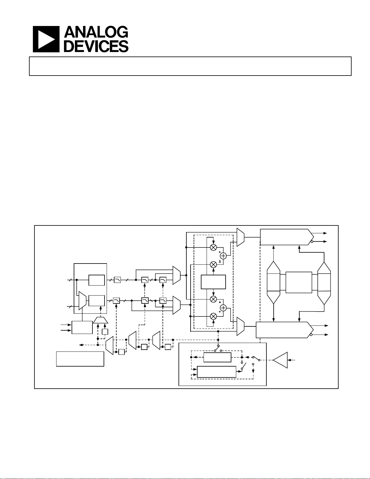
FUNCTIONAL BLOCK DIAGRAM
AD9775
Versatile input data interface
Twos complement/straight binary data coding
Dual-port or single-port interleaved input data
Single 3.3 V supply operation
Power dissipation: 1.2 W @ 3.3 V typical
On-chip, 1.2 V reference
80-lead, thin quad flat package, exposed pad (TQFP_EP)
APPLICATIONS
Communications
Analog quadrature modulation architecture
3G, multicarrier GSM, TDMA, CDMA systems
Broadband wireless, point-to-point microwave radios
Instrumentation/ATE
AD9775
I AND Q
NONINTERLEAVED
OR INTERLEAVED
DATA
WRITE
SELECT
CLOCK OUT
SPI INTERFACE AND
CONTROL REGISTERS
HALFBAND
DATA
ASSEMBLER
14
14
LATCH
LATCH
MUX
CONTROL
HALF-BAND FILTERS ALSO CAN BE
*
CONFIGURED FOR ZERO STUFFING ONLY
FILTER1*
I
16
Q
/2
16
/2
HALFBAND
FILTER2*
/2 /2
FILTER3*
161616
16
HALFBAND
COS
SIN
16
16
FILTER
BYPASS
MUX
PLL CLOCK MULTIPLIER AND CLOCK DIVIDER
f
/2, 4, 8
DAC
SIN
COS
f
)
(
DAC
PRESCALER
PHASE DETECTOR
AND VCO
Figure 1.
IMAGE
REJECTION/
DUAL DAC
MODE
BYPASS
MUX
GAIN
DAC
VREF
IDAC
IDAC
I/Q DAC
GAIN/OFFSET
REGISTERS
DIFFERENTIAL
CLK
OFFSET
DAC
I
OUT
IOFFSET
02858-001
Rev. E
Information furnished by Analog Devices is believed to be accurate and reliable. However, no
responsibility is assumed by Anal og Devices for its use, nor for any infringements of patents or ot her
rights of third parties that may result from its use. Specifications subject to change without notice. No
license is granted by implication or otherwise under any patent or patent rights of Analog Devices.
Trademarks and registered trademarks are the property of their respective owners.
One Technology Way, P.O. Box 9106, Norwood, MA 02062-9106, U.S.A.
Tel: 781.329.4700 www.analog.com
Fax: 781.461.3113 ©2006 Analog Devices, Inc. All rights reserved.

AD9775
TABLE OF CONTENTS
Features.............................................................................................. 1
Applications....................................................................................... 1
Functional Block Diagram .............................................................. 1
Revision History ............................................................................... 3
General Description ......................................................................... 4
Product Highlights....................................................................... 4
Specifications..................................................................................... 5
DC Specifications ......................................................................... 5
Dynamic Specifications ............................................................... 6
Digital Specifications ................................................................... 7
Digital Filter Specifications......................................................... 8
Absolute Maximum Ratings............................................................ 9
ESD Caution.................................................................................. 9
Thermal Resistance ...................................................................... 9
Pin Configuration and Function Descriptions........................... 10
Typical Performance Characteristics ........................................... 12
Terminology .................................................................................... 17
Mode Control (via SPI Port) ......................................................... 18
Register Descriptions ..................................................................... 19
Address 0x00............................................................................... 19
Address 0x01............................................................................... 19
Address 0x02............................................................................... 19
Address 0x03............................................................................... 20
Address 0x04............................................................................... 20
Address 0x05, Address 0x09 ..................................................... 20
Address 0x06, Address 0x0A..................................................... 20
Address 0x07, Address 0x0B..................................................... 20
Address 0x08, Address 0x0C..................................................... 20
Address 0x08, Address 0x0C..................................................... 20
Functional Description.................................................................. 21
Serial Interface for Register Control........................................ 21
General Operation of the Serial Interface............................... 21
Instruction Byte .......................................................................... 22
Serial Interface Port Pin Descriptions..................................... 22
MSB/LSB Transfers.....................................................................22
Notes on Serial Port Operation ................................................22
DAC Operation........................................................................... 24
1R/2R Mode ................................................................................ 25
Clock Input Configurations...................................................... 25
Programmable PLL .................................................................... 26
Power Dissipation....................................................................... 27
Sleep/Power-Down Modes........................................................ 28
Two-Port Data Input Mode ...................................................... 28
PLL Enabled, Two-Port Mode .................................................. 28
DATACLK Inversion.................................................................. 29
DATACLK Driver Strength....................................................... 29
PLL Enabled, One-Port Mode.................................................. 29
ONEPORTCLK Inversion......................................................... 29
ONEPORTCLK Driver Strength.............................................. 30
IQ Pairing.................................................................................... 30
PLL Disabled, Two-Port Mode................................................. 30
PLL Disabled, One-Port Mode................................................. 30
Digital Filter Modes ................................................................... 31
Amplitude Modulation.............................................................. 31
Modulation, No Interpolation.................................................. 32
Modulation, Interpolation = 2×............................................... 33
Modulation, Interpolation = 4×............................................... 34
Modulation, Interpolation = 8×............................................... 35
Zero Stuffing ............................................................................... 36
Interpolating (Complex Mix Mode)........................................ 36
Operations on Complex Signals............................................... 36
Complex Modulation and Image Rejection of Baseband
Signals .......................................................................................... 37
Image Rejection and Sideband Suppression of Modulated
Carriers ........................................................................................ 38
Applying the Output Configurations........................................... 42
Unbuffered Differential Output, Equivalent Circuit ............. 42
Differential Coupling Using a Transformer............................ 42
Differential Coupling Using an Op Amp................................ 43
Interfacing the AD9775 with the AD8345 Quadrature
Modulator.................................................................................... 43
Evaluation Board............................................................................ 44
Outline Dimensions....................................................................... 54
Ordering Guide .......................................................................... 54
Rev. E | Page 2 of 56

AD9775
REVISION HISTORY
12/06—Rev. D to Rev. E
Changes to Figure 52, Figure 54, Figure 55, and Figure 56 .......29
1/06—Rev. C to Rev. D
Updated Formatting..........................................................Universal
Changes to Figure 32 ....................................................................22
Changes to Figure 108 .................................................................. 55
Updated Outline Dimensions...................................................... 58
Changes to Ordering Guide......................................................... 58
6/04—Rev. B to Rev. C
Updated Layout.................................................................Universal
Changes to DC Specifications ....................................................... 5
Changes to Absolute Maximum Ratings...................................... 9
Changes to the DAC Operation Section .................................... 25
Inserted Figure 38.......................................................................... 25
Changes to Figure 40 ....................................................................26
Changes to Table 11 ...................................................................... 28
Changes to Programmable PLL Section..................................... 28
Changes to Figures 49, 50, and 51............................................... 29
Changes to the PLL Enabled, One-Port Mode Section............ 30
Changes to the PLL Disabled, One-Port Mode Section........... 31
Changes to the Ordering Guide .................................................. 57
Updated Outline Dimensions...................................................... 57
3/03—Rev. A to Rev. B
Changes to Register Description—Address 04h....................... 16
Changes to Equation 1.................................................................. 16
Changes to Figure 8....................................................................... 20
2/03—Rev. 0 to Rev. A
Edits to Features ...............................................................................1
Edits to DC Specifications ..............................................................3
Edits to Dynamic Specifications ....................................................4
Edits to Pin Function Descriptions ...............................................8
Edits to Table I............................................................................... 14
Edits to Register Description—Address 02h............................. 15
Edits to Register Description—Address 03h............................. 16
Edits to Register Description—Address 07h, 0Bh.................... 16
Edits to Equation 1........................................................................ 16
Edits to MSB/LSB Transfers......................................................... 18
Edits to Programmable PLL......................................................... 21
Added New Figure 14................................................................... 22
Renumbered Figures 15–69......................................................... 22
Added Two-Port Data Input Mode Section............................... 23
Edits to PLL Enabled, Two-Port Mode ...................................... 24
Edits to Figure 19 .......................................................................... 24
Edits to Figure 21 .......................................................................... 25
Edits to PLL Disabled, Two-Port Mode ..................................... 25
Edits to Figure 22 .......................................................................... 25
Edits to Figure 23 .......................................................................... 26
Edits to Figure 26a ........................................................................ 27
Edits to Complex Modulation and Image Rejection of Baseband
Signals............................................................................................. 31
Edits to Evaluation Board ............................................................ 39
Edits to Figures 56–59.................................................................. 40
Replaced Figures 60–69................................................................ 42
Updated Outline Dimensions...................................................... 49
Rev. E | Page 3 of 56

AD9775
GENERAL DESCRIPTION
The AD97751 is the 14-bit member of the AD977x pincompatible, high performance, programmable 2×/4×/8×
interpolating TxDAC+ family. The AD977x family features a
serial port interface (SPI) that provides a high level of
programmability, thus allowing for enhanced system-level
options. These options include selectable 2×/4×/8×
interpolation filters; f
/2, fS/4, or fS/8 digital quadrature
S
modulation with image rejection; a direct IF mode;
programmable channel gain and offset control; programmable
internal clock divider; straight binary or twos complement data
interface; and a single-port or dual-port data interface.
The selectable 2×/4×/8× interpolation filters simplify the
requirements of the reconstruction filters while simultaneously
enhancing the pass-band noise/distortion performance of
TxDAC+ devices. The independent channel gain and offset
adjust registers allow the user to calibrate LO feedthrough and
sideband suppression errors associated with analog quadrature
modulators. The 6 dB of gain adjustment range can also be used
to control the output power level of each DAC.
The AD9775 can perform f
/2, fS/4, and fS/8 digital modulation
S
and image rejection when combined with an analog quadrature
modulator. In this mode, the AD9775 accepts I and Q complex
data (representing a single or multicarrier waveform), generates
a quadrature modulated IF signal along with its orthogonal
representation via its dual DACs, and presents these two
reconstructed orthogonal IF carriers to an analog quadrature
modulator to complete the image rejection upconversion
process. Another digital modulation mode (that is, the direct IF
mode) allows the original baseband signal representation to be
frequency translated such that pairs of images fall at multiples
of one-half the DAC update rate.
The AD977x family includes a flexible clock interface that
accepts differential or single-ended sine wave or digital logic
inputs. An internal PLL clock multiplier is included and
generates the necessary on-chip high frequency clocks. It can
also be disabled to allow the use of a higher performance
external clock source. An internal programmable divider
simplifies clock generation in the converter when using an
external clock source. A flexible data input interface allows for
straight binary or twos complement formats and supports
single-port interleaved or dual-port data.
Dual high performance DAC outputs provide a differential
current output programmable over a 2 mA to 20 mA range.
1
Protected by U.S. Patent Numbers 5,568,145; 5,689,257; and 5,703,519. Other patents pending.
The AD9775 is manufactured on an advanced 0.35 micron
CMOS process, operates from a single supply of 3.1 V to 3.5 V,
and consumes 1.2 W of power.
Targeted at wide dynamic range, multicarrier and multistandard
systems, the superb baseband performance of the AD9775 is
ideal for wideband CDMA, multicarrier CDMA, multicarrier
TDMA, multicarrier GSM, and high performance systems
employing high order QAM modulation schemes. The image
rejection feature simplifies and can help reduce the number of
signal band filters needed in a transmit signal chain. The direct
IF mode helps to eliminate a costly mixer stage for a variety of
communications systems.
PRODUCT HIGHLIGHTS
1. The AD9775 is the 14-bit member of the AD977x pin-
compatible, high performance, programmable 2×/4×/8×
interpolating TxDAC+ family.
2. Direct IF transmission capability for 70 MHz + IFs through
a novel digital mixing process.
/2, fS/4, and fS/8 digital quadrature modulation and user-
3. f
S
selectable image rejection to simplify/remove cascaded
SAW filter stages.
4. A 2×/4×/8× user-selectable, interpolating filter eases data
rate and output signal reconstruction filter requirements.
5. User-selectable, twos complement/straight binary data
coding.
6. User-programmable, channel gain control over 1 dB range
in 0.01 dB increments.
7. User programmable channel offset control ±10% over the
FSR.
8. Ultrahigh speed 400 MSPS DAC conversion rate.
9. Internal clock divider provides data rate clock for easy
interfacing.
10. Flexible clock input with single-ended or differential input,
CMOS, or 1 V p-p LO sine wave input capability.
11. Low power: complete CMOS DAC operates on 1.2 W from
a 3.1 V to 3.5 V single supply. The 20 mA full-scale current
can be reduced for lower power operation and several sleep
functions are provided to reduce power during idle
periods.
12. On-chip voltage reference. The AD9775 includes a 1.20 V
temperature compensated band gap voltage reference.
13. 80-lead, thin quad flat package, exposed pad (TQFP_EP).
Rev. E | Page 4 of 56

AD9775
SPECIFICATIONS
DC SPECIFICATIONS
T
to T
MIN
Table 1.
Parameter Min Typ Max Unit
RESOLUTION 14 Bits
DC Accuracy1
ANALOG OUTPUT (for 1R and 2R Gain Setting Modes)
Offset Error −0.02 ±0.01 +0.02 % of FSR
Gain Error (with Internal Reference) −1.0 +1.0 % of FSR
Gain Matching −1.0 ±0.1 +1.0 % of FSR
Full-Scale Output Current2 2 20 mA
Output Compliance Range −1.0 +1.25 V
Output Resistance 200 kΩ
Output Capacitance 3 pF
Gain, Offset Cal DACs, Monotonicity Guaranteed
REFERENCE OUTPUT
Reference Voltage 1.14 1.20 1.26 V
Reference Output Current3 100 nA
REFERENCE INPUT
Input Compliance Range 0.1 1.25 V
Reference Input Resistance 7 kΩ
Small Signal Bandwidth 0.5 MHz
TEMPERATURE COEFFICIENTS
Offset Drift 0 ppm of FSR/°C
Gain Drift (with Internal Reference) 50 ppm of FSR/°C
Reference Voltage Drift ±50 ppm/°C
POWER SUPPLY
AVDD
CLKVDD
CLKVDD (PLL ON)
DVDD
Power Supply Rejection Ratio—AVDD ±0.4 % of FSR/V
OPERATING RANGE −40 +85 °C
1
Measured at I
2
Nominal full-scale current, I
3
Use an external amplifier to drive any external load.
4
100 MSPS f
5
400 MSPS f
, AVDD = 3.3 V, CLKVDD = 3.3 V, DVDD = 3.3 V, PLLVDD = 3.3 V, I
MAX
= 20 mA, unless otherwise noted.
OUTFS
Integral Nonlinearity −5 ±1.5 +5 LSB
Differential Nonlinearity −3 ±1.0 +3 LSB
Voltage Range 3.1 3.3 3.5 V
Analog Supply Current (I
I
in SLEEP Mode 23.3 26 mA
AVDD
AVDD
4
)
72.5 76 mA
Voltage Range 3.1 3.3 3.5 V
Clock Supply Current (I
Clock Supply Current (I
)4 8.5 10.0 mA
CLKVDD
) 23.5 mA
CLKVDD
Voltage Range 3.1 3.3 3.5 V
Digital Supply Current (I
)4 34 41 mA
DVDD
Nominal Power Dissipation 380 410 mW
5
P
DIS
P
IN PWDN 6.0 mW
DIS
driving a virtual ground.
OUTA
with f
DAC
OUT
= 50 MSPS, fS/2 modulation, PLL enabled.
DAC
, is 32 × the I
OUTFS
= 1 MHz, all supplies = 3.3 V, no interpolation, no modulation.
current.
REF
1.75 W
Rev. E | Page 5 of 56

AD9775
DYNAMIC SPECIFICATIONS
T
to T
MIN
transformer-coupled output, 50 Ω doubly terminated, unless otherwise noted.
Table 2.
Parameter Min Typ Max Unit
DYNAMIC PERFORMANCE
Maximum DAC Output Update Rate (f
Output Settling Time (tST) to 0.025% 11 ns
Output Rise Time 10% to 90%1 0.8 ns
Output Fall Time 10% to 90%
Output Noise, I
AC LINEARITY—BASEBAND MODE
Spurious-Free Dynamic Range (SFDR) to Nyquist (f
Spurious-Free Dynamic Range Within a 1 MHz Window
Two-Tone Intermodulation (IMD) to Nyquist (f
Total Harmonic Distortion (THD)
Signal-to-Noise Ratio (SNR)
Adjacent Channel Power Ratio (ACPR)
IF = Baseband, f
IF = 19.2 MHz, f
Four-Tone Intermodulation
AC LINEARITY—IF MODE
Four-Tone Intermodulation at IF = 200 MHz
1
Measured single-ended into 50 Ω load.
, AVDD = 3.3 V, CLKVDD = 3.3 V, DVDD = 3.3 V, PLLVDD = 0 V, I
MAX
) 400 MSPS
DAC
1
= 20 mA 50 pA/√Hz
OUTFS
= 0 dBFS)
OUT
f
= 100 MSPS, f
DATA
f
= 65 MSPS, f
DATA
f
= 65 MSPS, f
DATA
f
= 78 MSPS, f
DATA
f
= 78 MSPS, f
DATA
f
= 160 MSPS, f
DATA
f
= 160 MSPS, f
DATA
f
= 0 dBFS, f
OUT
f
= 65 MSPS, f
DATA
f
= 65 MSPS, f
DATA
f
= 78 MSPS, f
DATA
f
= 78 MSPS, f
DATA
f
= 160 MSPS, f
DATA
f
= 160 MSPS, f
DATA
f
= 100 MSPS, f
DATA
f
= 78 MSPS, f
DATA
f
= 160 MSPS, f
DATA
= 1 MHz 71 84.5 dBc
OUT
= 1 MHz 84 dBc
OUT
= 15 MHz 80 dBc
OUT
= 1 MHz 84 dBc
OUT
= 15 MHz 80 dBc
OUT
= 1 MHz 82 dBc
OUT
= 15 MHz 80 dBc
OUT
= 100 MSPS, f
DATA
= 10 MHz; f
OUT1
= 20 MHz; f
OUT1
= 10 MHz; f
OUT1
= 20 MHz; f
OUT1
= 10 MHz; f
OUT1
= 20 MHz; f
OUT1
= 1 MHz; 0 dBFS −71 −82.5 dB
OUT
= 5 MHz; 0 dBFS 76 dB
OUT
= 5 MHz; 0 dBFS 74 dB
OUT
= 1 MHz 73 91.3 dBc
OUT
= f
OUT1
= 11 MHz 81 dBc
OUT2
= 21 MHz 76 dBc
OUT2
= 11 MHz 81 dBc
OUT2
= 21 MHz 76 dBc
OUT2
= 11 MHz 81 dBc
OUT2
= 21 MHz 76 dBc
OUT2
= −6 dBFS)
OUT2
= 20 mA, interpolation = 2×, differential
OUTFS
0.8 ns
W-CDMA with 3.84 MHz BW, 5 MHz Channel Spacing
= 76.8 MSPS 71 dBc
DATA
= 76.8 MSPS 71 dBc
DATA
21 MHz, 22 MHz, 23 MHz, and 24 MHz at −12 dBFS (f
201 MHz, 202 MHz, 203 MHz, and 204 MHz at −12 dBFS (f
= MSPS, Missing Center) 75 dBFS
DATA
= 160 MSPS, f
DATA
= 320 MHz) 72 dBFS
DAC
Rev. E | Page 6 of 56

AD9775
DIGITAL SPECIFICATIONS
T
to T
MIN
, AVDD = 3.3 V, CLKVDD = 3.3 V, PLLVDD = 0 V, DVDD = 3.3 V, I
MAX
Table 3.
Parameter Min Typ Max Unit
DIGITAL INPUTS
Logic 1 Voltage 2.1 3 V
Logic 0 Voltage 0 0.9 V
Logic 1 Current −10 +10 μA
Logic 0 Current −10 +10 μA
Input Capacitance 5 pF
CLOCK INPUTS
Input Voltage Range 0 3 V
Common-Mode Voltage 0.75 1.5 2.25 V
Differential Voltage 0.5 1.5 V
SERIAL CONTROL BUS
Maximum SCLK Frequency (f
Minimum Clock Pulse Width High (t
Minimum Clock Pulse Width Low (t
) 15 MHz
SLCK
) 30 ns
PWH
) 30 ns
PWL
Maximum Clock Rise/Fall Time 1 ms
Minimum Data/Chip Select Setup Time (tDS) 25 ns
Minimum Data Hold Time (tDH) 0 ns
Maximum Data Valid Time (tDV) 30 ns
RESET Pulse Width 1.5 ns
Inputs (SDI, SDIO, SCLK, CSB)
Logic 1 Voltage 2.1 3 V
Logic 0 Voltage 0 0.9 V
Logic 1 Current −10 +10 μA
Logic 0 Current −10 +10 μA
Input Capacitance 5 pF
SDIO Output
Logic 1 Voltage DRVDD − 0.6 V
Logic 0 Voltage 0.4 V
Logic 1 Current 30 50 mA
Logic 0 Current 30 50 mA
= 20 mA, unless otherwise noted.
OUTFS
Rev. E | Page 7 of 56
AD9775
DIGITAL FILTER SPECIFICATIONS
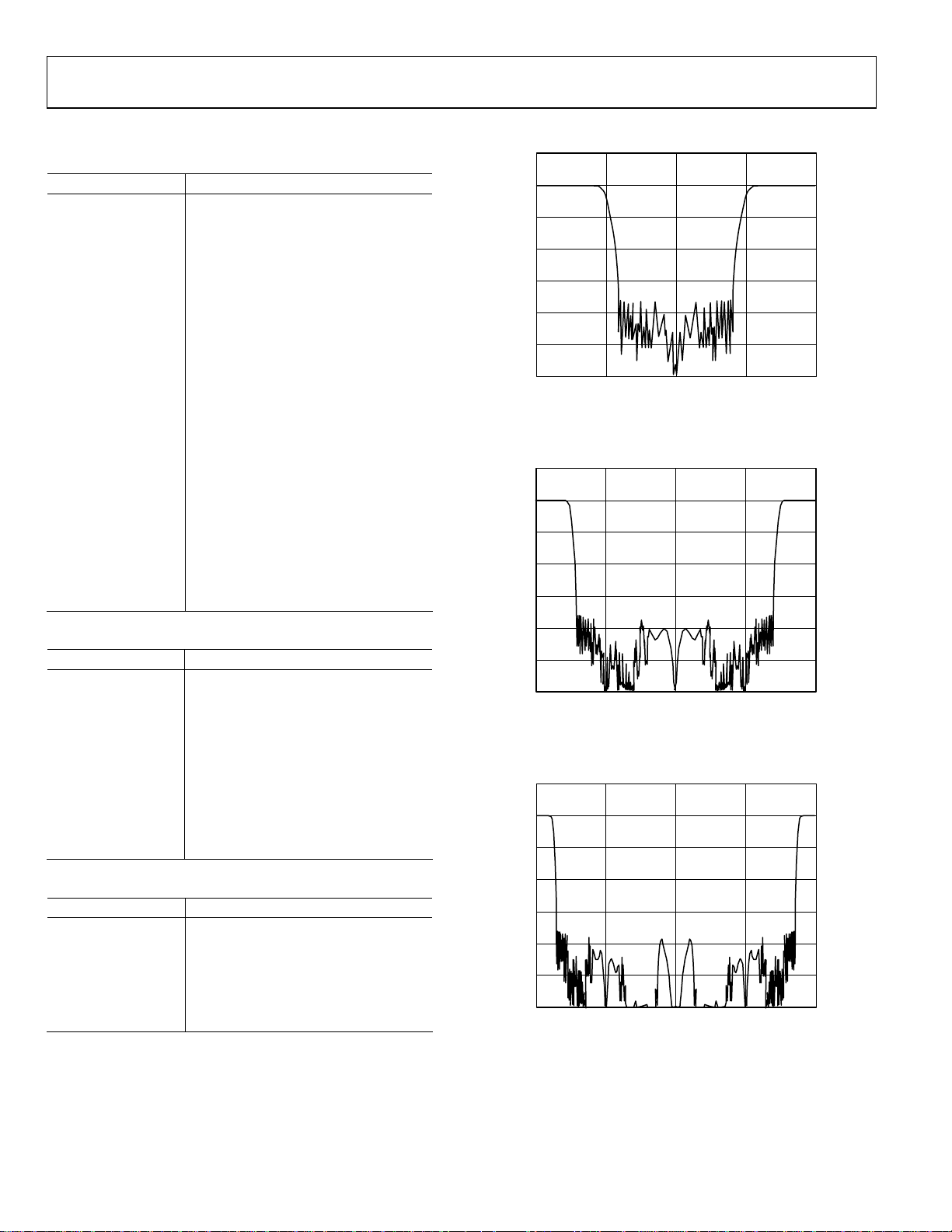
Table 4. Half-Band Filter No. 1 (43 Coefficients)
Tap Coefficient
1, 43 8
2, 42 0
3, 41 −29
4, 40 0
5, 39 67
6, 38 0
7, 37 −134
8, 36 0
9, 35 244
10, 34 0
11, 33 −414
12, 32 0
13, 31 673
14, 30 0
15, 29 −1079
16, 28 0
17, 27 1772
18, 26 0
19, 25 −3280
20, 24 0
21, 23 10,364
22 16,384
Table 5. Half-Band Filter No. 2 (19 Coefficients)
Tap Coefficient
1, 19 19
2, 18 0
3, 17 −120
4, 16 0
5, 15 438
6, 14 0
7, 13 −1288
8, 12 0
9, 11 5,047
10 8,192
20
0
–20
–40
–60
ATTENUATION (dBFS)
–80
–100
–120
f
OUT
Figure 2. 2× Interpolating Filter Response
20
0
–20
–40
–60
ATTENUATION (dBFS)
–80
–100
–120
f
OUT
Figure 3. 4× Interpolating Filter Response
20
0
–20
0.50 1.0 1.5 2.0
(NORMALIZED TO INPUT DATA RATE)
0.50 1.0 1.5 2.0
(NORMALIZED TO INPUT DATA RATE)
02858-002
02858-003
Table 6. Half-Band Filter No. 3 (11 Coefficients)
Tap Coefficient
1, 11 7
2, 10 0
3, 9 −53
4, 8 0
5, 7 302
6 512
Rev. E | Page 8 of 56
–40
–60
ATTENUATION (dBFS)
–80
–100
–120
f
OUT
Figure 4. 8× Interpolating Filter Response
2046
(NORMALIZED TO INPUT DATA RATE)
8
02858-004
AD9775
ABSOLUTE MAXIMUM RATINGS
Table 7.
Parameter With Respect To Rating
AVDD, DVDD, CLKVDD AGND, DGND, CLKGND −0.3 V to +4.0 V
AVDD, DVDD, CLKVDD AVDD, DVDD, CLKVDD −4.0 V to +4.0 V
AGND, DGND, CLKGND AGND, DGND, CLKGND −0.3 V to +0.3 V
REFIO, FSADJ1/FSADJ2 AGND −0.3 V to AVDD + 0.3 V
I
, I
OUTA
P1B13 to P1B0, P2B13 to P2B0, RESET DGND −0.3 V to DVDD + 0.3 V
DATACLK, PLL_LOCK DGND −0.3 V to DVDD + 0.3 V
CLK+, CLK– CLKGND −0.3 V to CLKVDD + 0.3 V
LPF CLKGND −0.3 V to CLKVDD + 0.3 V
SPI_CSB, SPI_CLK, SPI_SDIO, SPI_SDO DGND −0.3 V to DVDD + 0.3 V
Junction Temperature 125°C
Storage Temperature −65°C to +150°C
Lead Temperature (10 sec) 300°C
Stresses above those listed under Absolute Maximum Ratings
may cause permanent damage to the device. This is a stress
rating only; functional operation of the device at these or any
other conditions above those indicated in the operational
section of this specification is not implied. Exposure to absolute
maximum rating conditions for extended periods may affect
device reliability.
ESD CAUTION
AGND −1.0 V to AVDD + 0.3 V
OUTB
THERMAL RESISTANCE
θJA is specified for the worst-case conditions, that is, a device
soldered in a circuit board for surface-mount packages.
Table 8. Thermal Resistance
Package Type θJA Unit
80-Lead Thin Quad Flat Package
(TQFP_EP), Exposed Pad
23.5 °C/W
Rev. E | Page 9 of 56
AD9775
2
2
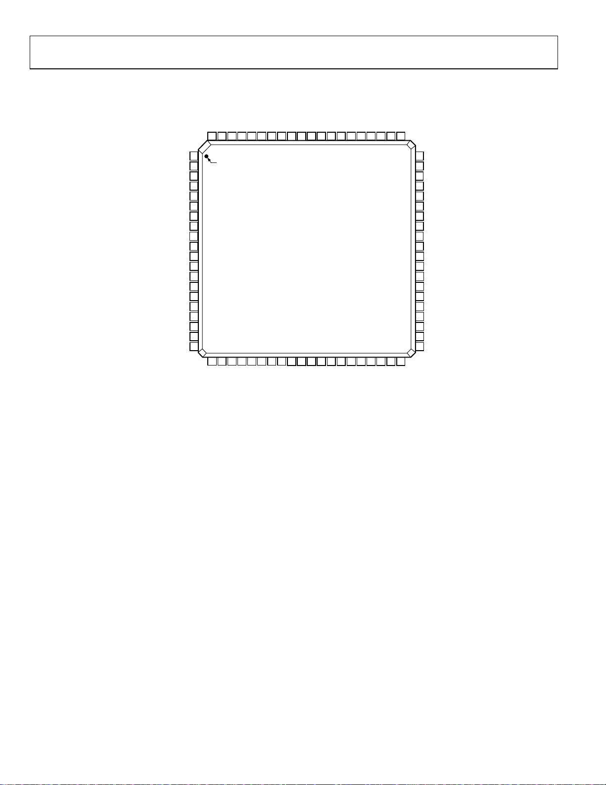
PIN CONFIGURATION AND FUNCTION DESCRIPTIONS
CLKVDD
LPF
CLKVDD
CLKGND
CLK+
CLK–
CLKGND
DATACLK/PLL_LOCK
DGND
DVDD
P1B13 (MSB)
P1B12
P1B11
P1B10
P1B9
P1B8
DGND
DVDD
P1B7
P1B6
NC = NO CONNECT
OUTA1
AVDD
AVDD
AGND
80 79 78 77 76 75 74 73 72 71 70 69 68 67 66 65 64 63 62 61
1
PIN 1
2
3
4
5
6
7
8
9
10
11
12
13
14
15
16
17
18
19
20
21 22 23 24 25 26 27 28 29 30 31 32 33 34 35 36 37 38 39 40
P1B5
P1B4
AVDD
AGND
AGND
P1B3
P1B2
DVDD
DGND
AGND
I
(Not to Scale)
P1B1
OUTB1
I
AD9775
TxDAC+
TOP VIEW
NC
AGND
NC
AGND
OUTA
I
OUTB
I
P2B11
AGND
P2B10
AGND
DGND
P1B0 (LSB)
AVDD
DVDD
AGND
AVDD
P2B9
P2B8
AGND
P2B7
AVDD
P2B6
60
FSADJ1
59
FSADJ2
58
REFIO
57
RESET
56
SPI_CSB
55
SPI_CLK
54
SPI_SDIO
53
SPI_SDO
52
DGND
51
DVDD
50
NC
49
NC
48
P2B0 (LSB)
47
P2B1
46
P2B2
45
P2B3
44
DGND
43
DVDD
42
P2B4
41
P2B5
IQSEL/P2B13 (MSB)
ONEPORTCLK/P2B12
Figure 5. Pin Configuration
02858-005
Rev. E | Page 10 of 56

AD9775
Table 9. Pin Function Descriptions
Pin No. Mnemonic Description
1, 3 CLKVDD Clock Supply Voltage.
2 LPF PLL Loop Filter.
4, 7 CLKGND Clock Supply Common.
5 CLK+ Differential Clock Input.
6 CLK− Differential Clock Input.
8 DATACLK/PLL_LOCK
9, 17, 25, 35, 44, 52 DGND Digital Common.
10, 18, 26, 36, 43, 51 DVDD Digital Supply Voltage.
11 to 16, 19 to 24, 27, 28
P1B13 (MSB) to P1B0
(LSB)
29, 30, 49, 50 NC No Connect.
31 IQSEL/P2B13 (MSB)
32 ONEPORTCLK/P2B12
33, 34, 37 to 42, 45 to 48 P2B11 to P2B0 (LSB) Port 2 Data Inputs.
53 SPI_SDO
54 SPI_SDIO
55 SPI_CLK
56 SPI_CSB
57 RESET
58 REFIO Reference Output, 1.2 V Nominal.
59 FSADJ2 Full-Scale Current Adjust, Q Channel.
60 FSADJ1 Full-Scale Current Adjust, I Channel.
61, 63, 65, 76, 78, 80 AVDD Analog Supply Voltage.
62, 64, 66, 67, 70, 71,
AGND Analog Common.
74, 75, 77, 79
68, 69 I
72, 73 I
, I
OUTB2
OUTA2
OUTB1, IOUTA1
Differential DAC Current Outputs, Q Channel.
Differential DAC Current Outputs, I Channel.
With the PLL enabled, this pin indicates the state of the PLL. A read of a Logic 1
indicates the PLL is in the locked state. Logic 0 indicates the PLL has not achieved
lock. This pin may also be programmed to act as either an input or output
(Address 02h, Bit 3) DATACLK signal running at the input data rate.
Port 1 Data Inputs.
In one-port mode, IQSEL = 1 followed by a rising edge of the differential input
clock latches the data into the I channel input register. IQSEL = 0 latches the data
into the Q channel input register. In two-port mode, this pin becomes the Port 2
MSB.
With the PLL disabled and the AD9775 in one-port mode, this pin becomes a
clock output that runs at twice the input data rate of the I and Q channels. This
allows the AD9775 to accept and demux interleaved I and Q data to the I and Q
input registers.
In the case where SDIO is an input, SDO acts as an output. When SDIO becomes an
output, SDO enters a High-Z state. This pin can also be used as an output for the
data rate clock. For more information, see the
Two-Port Data Input Mode section.
Bidirectional Data Pin. Data direction is controlled by Bit 7 of Register Address 0x00.
The default setting for this bit is 0, which sets SDIO as an input.
Data input to the SPI port is registered on the rising edge of SPI_CLK. Data output
on the SPI port is registered on the falling edge.
Chip Select/SPI Data Synchronization. On momentary logic high, resets SPI port
logic and initializes instruction cycle.
Logic 1 resets all of the SPI port registers, including Address 0x00, to their default
values. A software reset can also be done by writing a Logic 1 to SPI Register 00h,
Bit 5. However, the software reset has no effect on the bit in Address 0x00.
Rev. E | Page 11 of 56
AD9775
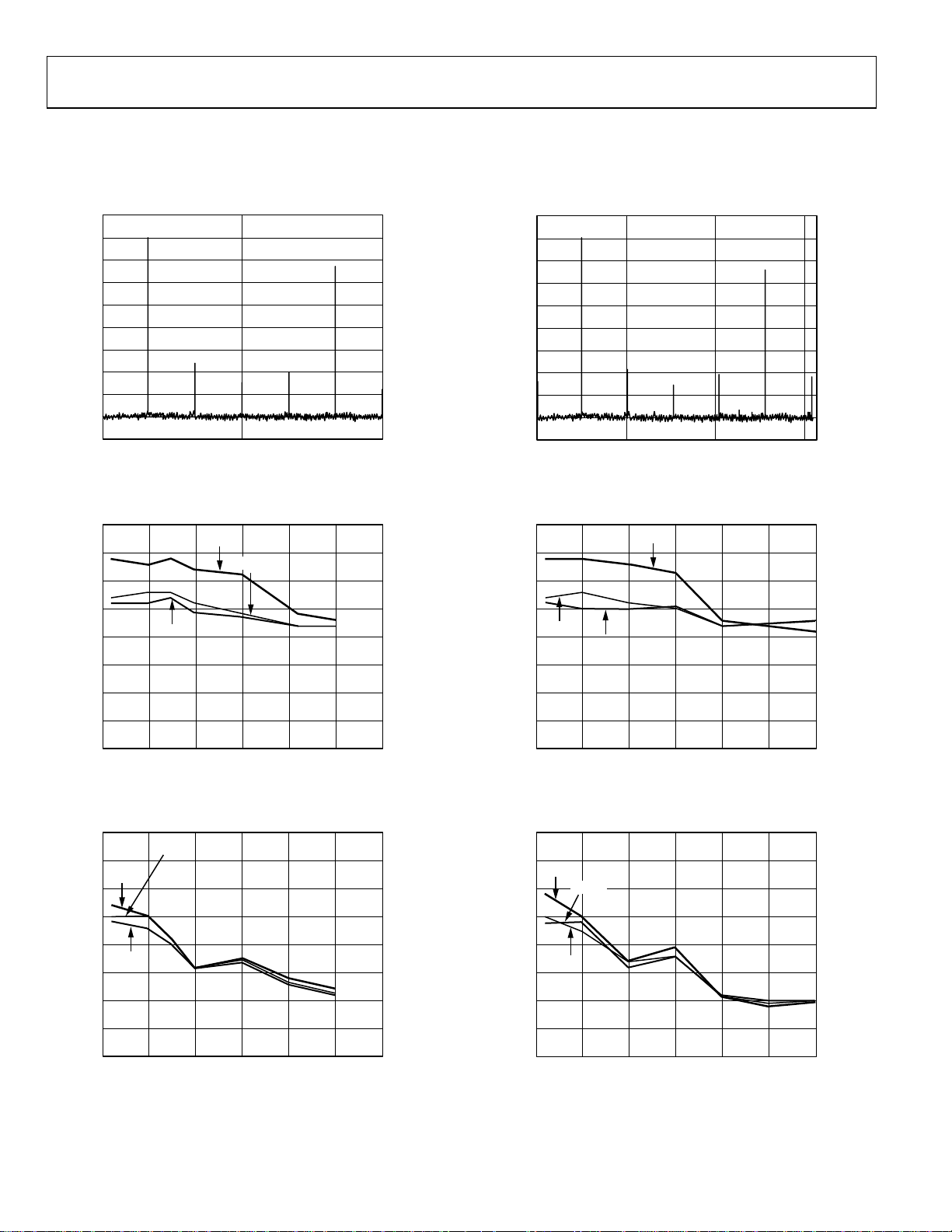
TYPICAL PERFORMANCE CHARACTERISTICS
T = 25°C, AVDD = 3.3 V, CLKVDD = 3.3 V, DVDD = 3.3 V, I
50 Ω doubly terminated, unless otherwise noted.
10
0
–10
–20
–30
–40
–50
AMPLITUDE (dBm)
–60
–70
–80
–90
0 65 130
FREQUENCY (MHz)
Figure 6. Single-Tone Spectrum @ f
90
0dBFS
85
80
= 65 MSPS with f
DATA
–6dBFS
OUT
= f
DATA
= 20 mA, interpolation = 2×, differential transformer-coupled output,
OUTFS
10
0
–10
–20
–30
–40
–50
AMPLITUDE (dBm)
–60
–70
–80
–90
0 10050 150
FREQUENCY (MHz)
= 78 MSPS with f
DATA
0dBFS
/3
02858-006
Figure 9. Single-Tone Spectrum @ f
90
85
80
OUT
= f
DATA
02858-009
/3
75
70
SFDR (dBc)
65
60
55
50
–12dBFS
Figure 7. In-Band SFDR vs. f
90
85
80
75
70
SFDR (dBc)
65
60
55
50
–6dBFS
0dBFS
–12dBFS
Figure 8. Out-of-Band SFDR vs. f
10 150 5 20 25 30
FREQUENCY (MHz)
@ f
OUT
@ f
DATA
DATA
= 65 MSPS
= 65 MSPS
OUT
10 150 5 20 25 30
FREQUENCY (MHz)
02858-007
02858-008
75
–12dBFS
70
SFDR (dBc)
65
60
55
50
–6dBFS
Figure 10. In-Band SFDR vs. f
90
85
–6dBFS
80
75
70
SFDR (dBc)
65
60
55
50
0dBFS
–12dBFS
Figure 11. Out-of-Band SFDR vs. f
10 150 5 20 25 30
FREQUENCY (MHz)
@ f
OUT
@ f
DATA
DATA
= 78 MSPS
= 78 MSPS
OUT
10 150 5 20 25 30
FREQUENCY (MHz)
02858-010
02858-011
Rev. E | Page 12 of 56
AD9775
10
0
–10
–20
–30
–40
–50
AMPLITUDE (dBm)
–60
–70
–80
–90
0 200100 300
FREQUENCY (MHz)
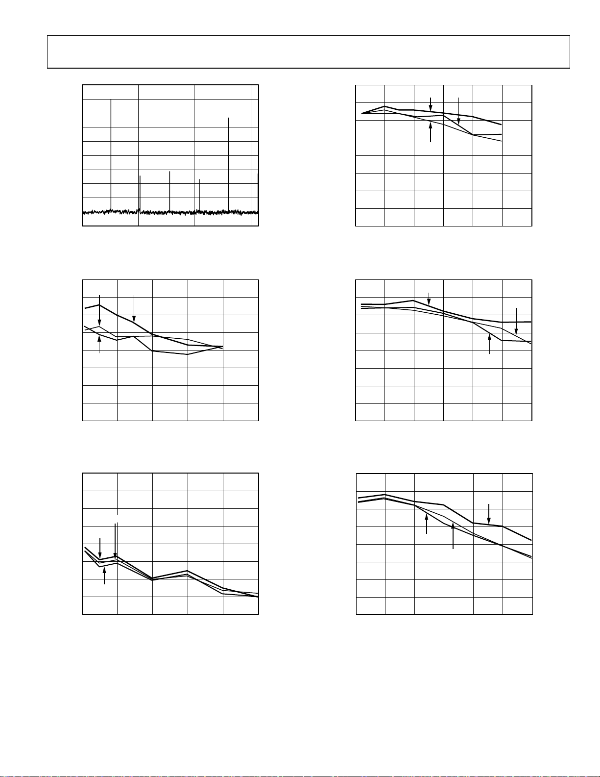
Figure 12. Single-Tone Spectrum @ f
90
–6dBFS
85
80
0dBFS
= 160 MSPS with f
DATA
OUT
= f
DATA
02858-012
/3
90
85
80
75
70
IMD (dBc)
65
60
55
50
–6dBFS
0dBFS
10 150 5 20 25 30
FREQUENCY (MHz)
Figure 15. Third-Order IMD Products vs. f
90
85
80
–6dBFS
–3dBFS
OUT
@ f
= 65 MSPS
DATA
0dBFS
02858-015
75
70
–12dBFS
SFDR (dBc)
65
60
55
50
0 1020304050
FREQUENCY (MHz)
Figure 13. In-Band SFDR vs. f
90
85
80
75
70
SFDR (dBc)
65
60
55
50
–6dBFS
0dBFS
–12dBFS
0 1020304050
FREQUENCY (MHz)
Figure 14. Out-of-Band SFDR vs. f
OUT
OUT
@ f
@ f
= 160 MSPS
DATA
= 160 MSPS
DATA
02858-013
02858-014
75
70
IMD (dBc)
65
60
55
50
10 150 5 20 25 30
FREQUENCY (MHz)
Figure 16. Third-Order IMD Products vs. f
90
85
80
75
70
IMD (dBc)
65
60
55
50
–3dBFS
20 300 10 405060
FREQUENCY (MHz)
Figure 17. Third-Order IMD Products vs. f
0dBFS
–3dBFS
@ f
OUT
–6dBFS
@ f
OUT
= 78 MSPS
DATA
= 160 MSPS
DATA
02858-016
02858-017
Rev. E | Page 13 of 56
AD9775
90
×
85
8
90
–3dBFS
85
80
75
70
IMD (dBc)
65
60
55
50
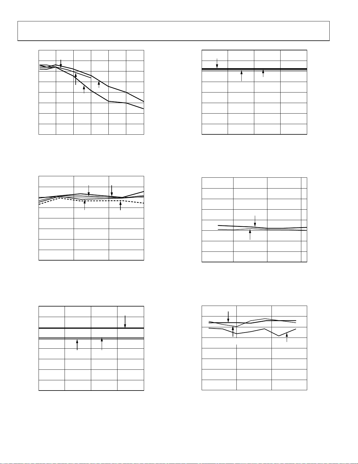
Figure 18. Third-Order IMD Products vs. f
= 160 MSPS, 2× f
1× f
DATA
90
85
80
75
70
IMD (dBc)
65
60
55
50
–15 –5–10 0
Figure 19. Third-Order IMD Products vs. A
= 50 MSPS for All Cases, 1× f
f
DATA
4× f
4
×
20 300 10 405060
FREQUENCY (MHz)
8× f
= 200 MSPS, 8× f
DAC
2
×
1
×
= 160 MSPS, 4× f
DATA
= 50 MSPS
DATA
4×
2×
(dBFS)
A
OUT
= 50 MSPS, 2× f
DAC
DAC
and Interpolation Rate,
OUT
DATA
8×
1×
and Interpolation Rate,
OUT
= 400 MSPS
= 80 MSPS,
= 100 MSPS,
DAC
02858-018
02858-019
80
75
70
SFDR (dBc)
65
60
55
50
–6dBFS
3.23.1 3.3 3.4 3.5
0dBFS
AVDD (V)
Figure 21. Third-Order IMD Products vs. AVDD @ f
f
= 320 MSPS, f
DAC
90
85
80
75
70
SNR (dB)
65
60
55
50
0 10050 150
PLL ON
INPUT DATA RATE (MSPS)
Figure 22. SNR vs. Data Rate for f
DATA
PLL OFF
= 160 MSPS
OUT
OUT
= 5 MHz
= 10 MHz,
02858-021
02858-022
90
85
80
75
70
SFDR (dBc)
65
60
55
50
–12dBFS
3.23.1 3.3 3.4 3.5
Figure 20. SFDR vs. AVDD @ f
AVDD (V)
= 10 MHz, f
OUT
–6dBFS
DAC
0dBFS
= 320 MSPS, f
= 160 MSPS
DATA
02858-020
Rev. E | Page 14 of 56
90
85
80
75
70
SFDR (dBc)
65
60
55
50
–50 500 100
78MSPS
f
= 65MSPS
DATA
°
TEMPERATURE (
C)
Figure 23. SFDR vs. Temperature @ f
160MSPS
= f
OUT
DATA
/11
02858-023
AD9775
0
–10
–20
–30
–40
–50
–60
AMPLITUDE (dBm)
–70
–80
–90
–100
0 10050 150
FREQUENCY (MHz)
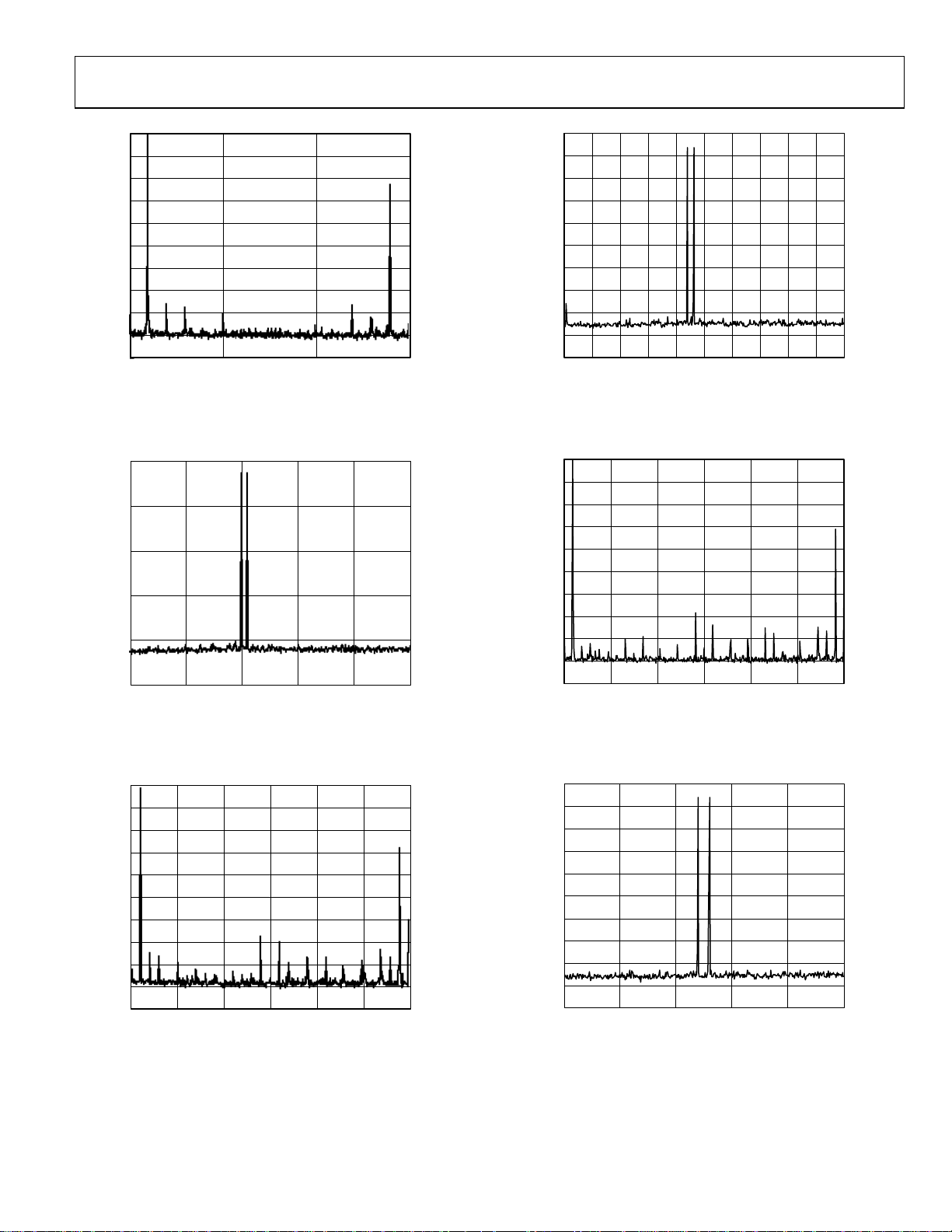
Figure 24. Single-Tone Spurious Performance, f
= 150 MSPS, No Interpolation
f
DATA
= 10 MHz,
OUT
02858-024
0
–10
–20
–30
–40
–50
–60
AMPLITUDE (dBm)
–70
–80
–90
–100
0 5 10 15 20 25 30 35 40 45 50
FREQUENCY (MHz)
Figure 27. Two-Tone IMD Performance, f
= 150 MSPS, Interpolation = 4×
DATA
02858-027
0
–20
–40
–60
AMPLITUDE (dBm)
–80
–100
01020304050
FREQUENCY (MHz)
Figure 25. Two-Tone IMD Performance, f
0
–10
–20
–30
–40
–50
–60
AMPLITUDE (dBm)
–70
–80
–90
–100
100 1500 50 200 250 300
FREQUENCY (MHz)
Figure 26. Single-Tone Spurious Performance, f
f
= 150 MSPS, Interpolation = 2×
DATA
= 150 MSPS, No Interpolation
DATA
= 10 MHz,
OUT
02858-025
02858-026
0
–10
–20
–30
–40
–50
–60
AMPLITUDE (dBm)
–70
–80
–90
–100
100 1500 50 200 250 300
FREQUENCY (MHz)
Figure 28. Single-Tone Spurious Performance, f
f
= 80 MSPS, Interpolation = 4×
DATA
0
–10
–20
–30
–40
–50
–60
AMPLITUDE (dBm)
–70
–80
–90
–100
0 5 10 15 20 25
FREQUENCY (MHz)
Figure 29. Two-Tone IMD Performance, f
= 50 MSPS, Interpolation = 8×
f
DATA
OUT
= 10 MHz,
OUT
= 10 MHz,
02858-028
02858-029
Rev. E | Page 15 of 56
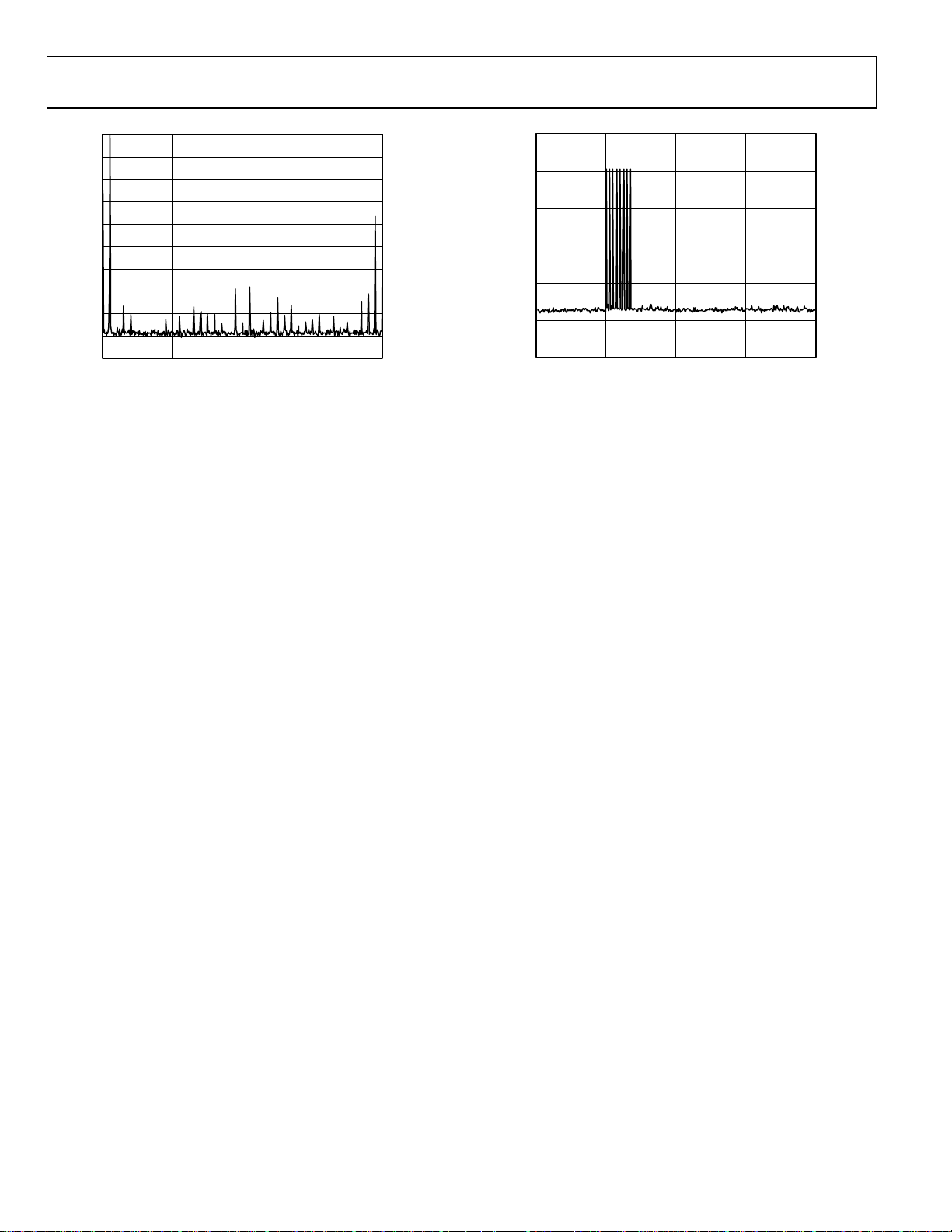
AD9775
0
–10
–20
–30
–40
–50
–60
AMPLITUDE (dBm)
–70
–80
–90
–100
1000 200 300 400
FREQUENCY (MHz)
Figure 30. Single-Tone Spurious Performance, f
= 50 MSPS, Interpolation = 8×
f
DATA
= 10 MHz,
OUT
02858-030
0
–20
–40
–60
–80
AMPLITUDE (dBm)
–100
–120
2004060
FREQUENCY (MHz)
Figure 31. Eight-Tone IMD Performance, f
Interpolation = 8×
= 160 MSPS,
DATA
80
02858-031
Rev. E | Page 16 of 56

AD9775
TERMINOLOGY
Adjacent Channel Power Ratio (ACPR)
A ratio in dBc between the measured power within a channel
relative to its adjacent channel.
Complex Image Rejection
In a traditional two-part upconversion, two images are created
around the second IF frequency. These images are redundant
and have the effect of wasting transmitter power and system
bandwidth. By placing the real part of a second complex
modulator in series with the first complex modulator, either the
upper or lower frequency image near the second IF can be
rejected.
Complex Modulation
The process of passing the real and imaginary components of a
signal through a complex modulator (transfer function = e
jωt
=
cosωt + jsinωt) and realizing real and imaginary components
on the modulator output.
Differential Nonlinearity (DNL)
DNL is the measure of the variation in analog value, normalized
to full scale, associated with a 1 LSB change in digital input
code.
Gain Error
The difference between the actual and ideal output span. The
actual span is determined by the output when all inputs are set
to 1 minus the output when all inputs are set to 0.
Glitch Impulse
Asymmetrical switching times in a DAC give rise to undesired
output transients that are quantified by a glitch impulse. It is
specified as the net area of the glitch in pV-s.
Group Delay
Number of input clocks between an impulse applied at the
device input and the peak DAC output current. A half-band FIR
filter has constant group delay over its entire frequency range.
Impulse Response
Response of the device to an impulse applied to the input.
Interpolation Filter
If the digital inputs to the DAC are sampled at a multiple rate of
(interpolation rate), a digital filter can be constructed with
f
DATA
a sharp transition band near fDATA/2. Images that would
typically appear around f
(output data rate) can be greatly
DAC
suppressed.
Linearity Error
(Also called integral nonlinearity or INL.) It is defined as the
maximum deviation of the actual analog output from the ideal
output, determined by a straight line drawn from zero scale to
full scale.
Monotonicity
A DAC is monotonic if the output either increases or remains
constant as the digital input increases.
Offset Error
The deviation of the output current from the ideal of 0 is called
offset error. For I
are all 0. For I
, 0 mA output is expected when the inputs
OUTA
, 0 mA output is expected when all inputs are
OUTB
set to 1.
Output Compliance Range
The range of allowable voltage at the output of a current output
DAC. Operation beyond the maximum compliance limits may
cause either output stage saturation or breakdown, resulting in
nonlinear performance.
Pass Band
Frequency band in which any input applied therein passes
unattenuated to the DAC output.
Power Supply Rejection
The maximum change in the full-scale output as the supplies
are varied from minimum to maximum specified voltages.
Settling Time
The time required for the output to reach and remain within a
specified error band about its final value, measured from the
start of the output transition.
Signal-to-Noise Ratio (SNR)
SNR is the ratio of the rms value of the measured output signal
to the rms sum of all other spectral components below the
Nyquist frequency, excluding the first six harmonics and dc.
The value for SNR is expressed in decibels.
Spurious-Free Dynamic Range
The difference, in dB, between the rms amplitude of the output
signal and the peak spurious signal over the specified
bandwidth.
Stop-Band Rejection
The amount of attenuation of a frequency outside the pass band
applied to the DAC, relative to a full-scale signal applied at the
DAC input within the pass band.
Tem p er at u re Dr i ft
Temperature drift is specified as the maximum change from the
ambient (25°C) value to the value at either T
MIN
or T
MAX
. For
offset and gain drift, the drift is reported in ppm of full-scale
range (FSR) per °C. For reference drift, the drift is reported in
ppm per °C.
Total Harmonic Distortion (THD)
THD is the ratio of the rms sum of the first six harmonic
components to the rms value of the measured fundamental. It is
expressed as a percentage or in decibels (dB).
Rev. E | Page 17 of 56
 Loading...