

14-Bit, 32 MSPS TxDAC+™
VCO
IN/EXT
PLL
DIVIDE
PLLCOM
REFLO
PLL CLOCK
MULTIPLIER
REFIO
SNOOZE
IOUTA
FSADJ
AD9774
SLEEP
DCOM
DVDD
ICOMP ACOM AVDD
+1.2V REFERENCE
AND CONTROL AMP
PLL
ENABLE
PLLLOCK
CLK43IN
PLLVDD
LPF
IOUTB
EDGE
TRIGGERED
LATCHES
14
14-BIT
DAC
DATA
INPUTS
(DB13-DB0)
23 23
13 23 43
43
14
14
14
CLK IN/OUT
REFCOMP
a
FEATURES
Single 3 V or 5 V Supply
14-Bit DAC Resolution and Input Data Width
32 MSPS Input Data Rate at 5 V
13.5 MHz Reconstruction Bandwidth
12 ENOBS @ 1 MHz
77 dBc SFDR @ 5 MHz
4ⴛ Interpolation Filter
69 dB Image Rejection
84% Passband to Nyquist Ratio
0.002 dB Passband Ripple
23 3/4 Cycle Latency
Internal 4ⴛ Clock Multiplier
On-Chip 1.20 V Reference
44-Lead MQFP Package
APPLICATIONS
Communication Transmit Channel:
Wireless Basestations
ADSL/HFC Modems
Direct Digital Synthesis (DDS)
PRODUCT DESCRIPTION
The AD9774 is a single supply, oversampling, 14-bit digital-toanalog converter (DAC) optimized for waveform reconstruction
applications requiring exceptional dynamic range. Manufactured on an advanced CMOS process, it integrates a complete,
low distortion 14-bit DAC with a 4× digital interpolation filter
and clock multiplier. The two-stage, 4× digital interpolation
filter provides more than a six-fold reduction in the complexity
of the analog reconstruction-filter. It does so by multiplying the
input data rate by a factor of four while simultaneously suppressing
the original inband images by more than 69 dB. The on-chip
clock multiplier provides all the necessary clocks. The AD9774
can reconstruct full-scale waveforms having bandwidths as high
as 13.5 MHz when operating at an input data rate of 32 MSPS
and a DAC output rate of 128 MSPS.
The 14-bit DAC provides differential current outputs to support
differential or single-ended applications. A segmented current
source architecture is combined with a proprietary switching technique to reduce spurious components and enhance dynamic performance. Matching between the two current outputs ensures
enhanced dynamic performance in a differential output configuration. The differential current outputs may be fed into a transformer
or tied directly to an output resistor to provide two complementary,
single-ended voltage outputs. A differential op amp topology can
also be used to obtain a single-ended output voltage. The output
voltage compliance range is nominally 1.25 V.
TxDAC+ is a trademark of Analog Devices, Inc.
REV. B
Information furnished by Analog Devices is believed to be accurate and
reliable. However, no responsibility is assumed by Analog Devices for its
use, nor for any infringements of patents or other rights of third parties
which may result from its use. No license is granted by implication or
otherwise under any patent or patent rights of Analog Devices.
with 4ⴛ Interpolation Filters
AD9774
FUNCTIONAL BLOCK DIAGRAM
Edge-triggered input latches, a 4× clock multiplier, and a tem-
perature compensated bandgap reference have also been integrated to provide a complete monolithic DAC solution. Flexible
supply options support +3 V and +5 V CMOS logic families.
TTL logic levels can also be accommodated by reducing the
AD9774 digital supply.
The on-chip reference and control amplifier are configured for
maximum accuracy and flexibility. The AD9774 can be driven
by the on-chip reference or by a variety of external reference
voltages. The full-scale current of the AD9774 can be adjusted
over a 2 mA to 20 mA range, thus providing additional gain
ranging capabilities.
The AD9774 is available in a 44-lead MQFP package. It is
specified for operation over the industrial temperature range.
PRODUCT HIGHLIGHTS
1. On-Chip 4× interpolation filter eases analog reconstruction
filter requirements by suppressing the first three images by 69 dB.
2. Low glitch and fast settling time provide outstanding dynamic
performance for waveform reconstruction or digital synthesis
requirements, including communications.
3. On-chip, edge-triggered input CMOS latches interface readily
to CMOS and TTL logic families. The AD9774 can support
input data rates up to 32 MSPS.
4. A temperature compensated, 1.20 V bandgap reference is
included on-chip, providing a complete DAC solution. An
external reference may also be used.
5. The current output(s) of the AD9774 can easily be configured
for various single-ended or differential circuit topologies.
6. On-chip clock multiplier generates all the high-speed clocks
required by the internal interpolation filters. Both 2× and 4×
clocks are generated from the lower rate data clock supplied
by the user.
One Technology Way, P.O. Box 9106, Norwood, MA 02062-9106, U.S.A.
Tel: 781/329-4700 World Wide Web Site: http://www.analog.com
Fax: 781/326-8703 © Analog Devices, Inc., 1998

AD9774–SPECIFICATIONS
DC SPECIFICATIONS
(T
to T
MIN
, AVDD = +5 V, PLLVDD = +5 V, DVDD = +5 V, I
MAX
= 20 mA, unless otherwise noted)
OUTFS
Parameter Min Typ Max Units
RESOLUTION 14 Bits
DC ACCURACY
1
Integral Linearity Error (INL)
T
= +25°C ±4 LSB
A
to T
T
MIN
MAX
Differential Nonlinearity (DNL)
= +25°C ±3 LSB
T
A
T
to T
MIN
MAX
Monotonicity (12-Bit) GUARANTEED OVER RATED SPECIFICATION TEMPERATURE RANGE
ANALOG OUTPUT
Offset Error –0.025 +0.025 % of FSR
Gain Error (Without Internal Reference) –7 ±1 +7 % of FSR
Gain Error (With Internal Reference) +7.5 ±1 +7.5 % of FSR
Full-Scale Output Current
2
20 mA
Output Compliance Range 1.25 V
Output Resistance 100 kΩ
Output Capacitance 5 pF
REFERENCE OUTPUT
Reference Voltage 1.14 1.20 1.26 V
Reference Output Current
3
1 µA
REFERENCE INPUT
Input Compliance Range 0.1 1.25 V
Reference Input Resistance 1 MΩ
TEMPERATURE COEFFICIENTS
Unipolar Offset Drift 0 ppm of FSR/°C
Gain Drift (Without Internal Reference) ±50 ppm of FSR/°C
Gain Drift (With Internal Reference) ±100 ppm of FSR/°C
Reference Voltage Drift ±100 ppm of FSR/°C
POWER SUPPLY
AVDD
Voltage Range
Analog Supply Current (I
Analog Supply Current in SLEEP Mode (I
4
) 26.5 32 mA
AVDD
) 3.2 5 mA
AVDD
2.7 5.0 5.5 V
PLLVDD
Voltage Range 2.7 5.0 5.5 V
Clock Multiplier Supply Current (I
)1317mA
PLLVDD
DVDD
Voltage Range 2.7 5.0 5.5 V
Digital Supply Current at 5 V (I
Digital Supply Current at 5 V in SNOOZE Mode (I
Digital Supply Current at 3 V (I
Nominal Power Dissipation
AVDD and DVDD at 3 V
AVDD and DVDD at 5 V
6
6
Power Supply Rejection Ratio (PSRR)
Power Supply Rejection Ratio (PSRR)
5
DVDD
DVDD
)
) 42.0 50.0 mA
5
)
DVDD
123.0 140.0 mA
62.0 mA
415 mW
7
– AVDD –0.2 +0.2 % of FSR/V
7
– PLLVDD –0.025 +0.025 % of FSR/V
1125 mW
Power Supply Rejection Ratio (PSRR)7 – DVDD –0.025 +0.025 % of FSR/V
OPERATING RANGE –40 +85 °C
NOTES
1
Measured at IOUTA driving a virtual ground.
2
Nominal full-scale current, IOUTFS, is 32 × the I
3
Use an external amplifier to drive any external load.
4
For operation below 3 V, it is recommended that the output current be reduced to 12 mA or less to maintain optimum performance.
5
Measured at f
6
Measured as unbuffered voltage output into 50 Ω R
7
±5% power supply variation.
Specifications subject to change without notice.
= 25 MSPS and f
CLOCK
= 1.01 MHz.
OUT
current.
REF
at IOUTA and IOUTB, f
LOAD
= 32 MSPS and f
CLOCK
= 12.8 MHz.
OUT
–2–
REV. B
AD9774
(T
to T
, AVDD = +5 V, PLLVDD = +5 V, DVDD = +5 V, I
MAX
DYNAMIC SPECIFICATIONS
MIN
Coupled Output, 50 ⍀ Doubly Terminated, unless otherwise noted)
Parameter Min Typ Max Units
DYNAMIC PERFORMANCE
Maximum Output Update Rate w/DVDD = 5 V 128 MSPS
Maximum Output Update Rate w/DVDD = 3 V 100 128 MSPS
Output Settling Time (t
Output Propagation Delay (t
Glitch Impulse 5 pV-s
Output Rise Time (10% to 90%)
Output Fall Time (10% to 90%)
Output Noise (I
OUTFS
) (to 0.025%) 35 ns
ST
) 55 Clocks
PD
1
1
2.5 ns
2.5 ns
= 20 mA) 50 pA/√Hz
AC LINEARITY TO NYQUIST
Spurious-Free Dynamic Range (SFDR) to Nyquist
= 25 MSPS; f
f
CLOCK
= 1.01 MHz
OUT
0 dBFS Output 79 dB
–6 dBFS Output 86 dB
–12 dBFS Output 75 dB
–18 dBFS Output 75 dB
= 32 MSPS; f
f
CLOCK
= 32 MSPS; f
f
CLOCK
f
= 32 MSPS; f
CLOCK
f
= 32 MSPS; f
CLOCK
= 1.01 MHz 78 dB
OUT
= 5.01 MHz 77 dB
OUT
= 10.01 MHz 79 dB
OUT
= 13.01 MHz 78 dB
OUT
Total Harmonic Distortion (THD)
= 25 MSPS; f
f
CLOCK
= 1.01 MHz; 0 dBFS –75 dB
OUT
Signal-to-Noise Ratio (SNR)
f
= 25 MSPS; f
CLOCK
NOTES
1
Propagation delay is delay from data input to DAC update.
2
Measured single-ended into 50 Ω load.
Specifications subject to change without notice.
= 1.01 MHz; 0 dBFS 76 dB
OUT
= 20 mA, Differential Transformer
OUTFS
1
2
DIGITAL SPECIFICATIONS
MIN
, AVDD = +5 V, PLLVDD = +5 V, DVDD = +5 V, I
MAX
= 20 mA unless otherwise noted)
OUTFS
(T
to T
Parameter Min Typ Max Units
DIGITAL INPUTS
Logic “1” Voltage @ DVDD = +5 V 3.5 5 V
Logic “1” Voltage @ DVDD = +3 V 2.1 3 V
Logic “0” Voltage @ DVDD = +5 V 0 1.3 V
Logic “0” Voltage @ DVDD = +3 V 0 0.9 V
Logic “1” Current –10 +10 µA
Logic “0” Current –10 +10 µA
Input Capacitance 5 pF
Input Setup Time (t
Input Hold Time (t
Latch Pulsewidth (t
) 2.5 ns
S
) 1.5 ns
H
)4ns
LPW
DB0–DB11
CLOCK
IOUTA
OR
IOUTB
t
S
t
PD
t
t
0.025%
LPW
ST
t
H
0.025%
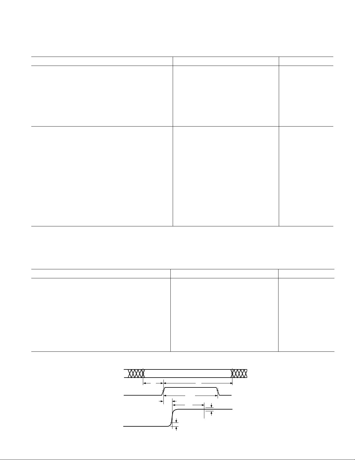
Figure 1. Timing Diagram
–3–REV. B
AD9774–SPECIFICATIONS
(T
to T
, AVDD = +2.7 V to +5.5 V, DVDD = +2.7 V to +5.5 V, I
MAX
DIGITAL FILTER SPECIFICATIONS
MIN
otherwise noted)
Parameter Min Typ Max Units
MAXIMUM INPUT CLOCK RATE (f
CLOCK
)
DVDD = 5 V 32 MSPS
DVDD = 3 V 25 32 MSPS
= 20 mA unless
OUTFS
DIGITAL FILTER CHARACTERISTICS
Passband Width
Passband Width: 0.01 dB 0.414 f
Passband Width: 0.1 dB 0.420 f
Passband Width: –3 dB 0.482 f
1
: 0.005 dB 0.410 f
OUT/fCLOCK
OUT/fCLOCK
OUT/fCLOCK
OUT/fCLOCK
LINEAR PHASE (FIR IMPLEMENTATION)
STOPBAND REJECTION
CLOCK
CLOCK
to 3.419 f
to 1.409 f
0.591 f
0.591 f
GROUP DELAY
CLOCK
CLOCK
2
–69.5 dB
–79.5 dB
38 Input Clocks
IMPULSE RESPONSE DURATION
–40 dB 53 Input Clocks
–60 dB 62 Input Clocks
NOTES
1
Excludes sinx/x characteristic of DAC.
2
Defined as the number of data clock cycles between impulse input and peak of output response.
Specifications subject to change without notice.
ABSOLUTE MAXIMUM RATINGS*
With
Respect
Parameter to Min Max Units
AVDD ACOM –0.3 +6.5 V
DVDD DCOM –0.3 +6.5 V
PLLVDD PLLCOM –0.3 +6.5 V
ACOM DCOM –0.3 +0.3 V
PLLCOM ACOM –0.3 +0.3 V
PLLCOM DCOM –0.3 +0.3 V
AVDD DVDD –6.5 +6.5 V
PLLVDD DVDD –0.3 +6.5 V
PLLVDD AVDD –0.3 +6.5 V
Model Range Description Option*
AD9774AS –40°C to +85°C 44-Lead MQFP S-44
AD9774EB Evaluation Board
*S = Metric Quad Flatpack.
THERMAL CHARACTERISTIC
Thermal Resistance
44-Lead MQFP
= 53.2°C/W
θ
JA
θ
= 19°C/W
JC
ORDERING GUIDE
Temperature Package Package
CLKIN, CLK4×IN DVDD –0.3 +6.5 V
SLEEP, SNOOZE DCOM –0.3 DVDD + 0.3 V
Digital Inputs DCOM –0.3 DVDD + 0.3 V
PLL DIVIDE, LPF ACOM –0.3 PLLVDD + 0.3 V
PLLLOCK ACOM –0.3 PLLVDD + 0.3 V
VCO IN/EXT ACOM –0.3 PLLVDD + 0.3 V
IOUTA/IOUTB ACOM –0.3 AVDD + 0.3 V
REFIO, FSADJ ACOM –0.3 AVDD + 0.3 V
FSADJ ACOM –0.3 AVDD + 0.3 V
ICOMP ACOM –0.3 AVDD + 0.3 V
REFCOM ACOM –0.3 +0.3 V
Junction Temperature +150 °C
Storage Temperature –65 +150 °C
Lead Temperature +300 °C
(10 sec)
*Stresses above those listed under Absolute Maximum Ratings may cause perma-
nent damage to the device. This is a stress rating only; functional operation of the
device at these or any other conditions above those indicated in the operational
sections of this specification is not implied. Exposure to absolute maximum ratings
for extended periods may effect device reliability.
–4–
REV. B
AD9774
WARNING!
ESD SENSITIVE DEVICE
0
–20
–40
–60
–80
–100
–120
OUTPUT – dBFS
–140
–160
–180
0 0.5
FREQUENCY – DC TO 23 f
1.0
1.5
CLOCK
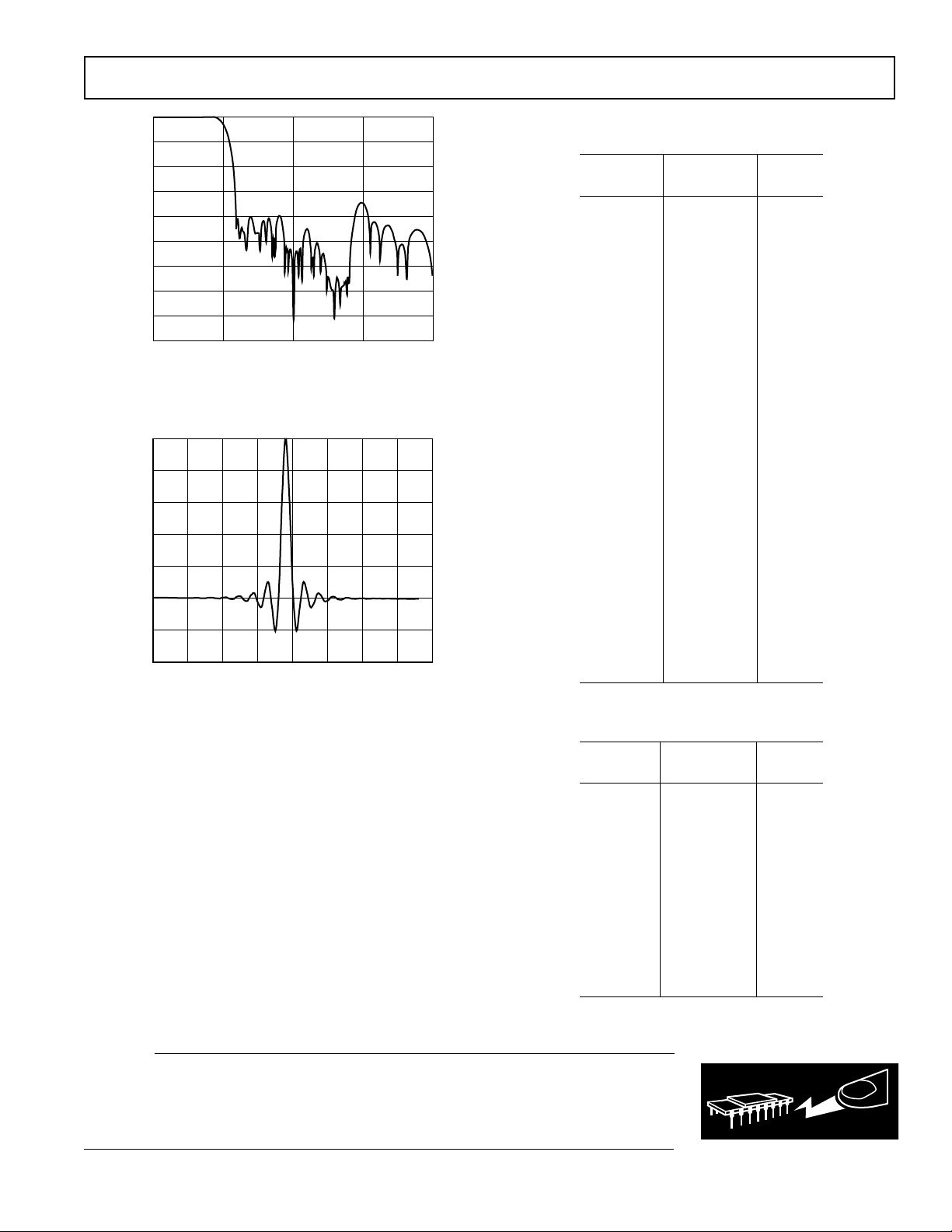
Figure 2a. FIR Filter Frequency Response
1.0
0.8
0.6
0.4
0.2
NORMALIZED OUTPUT
0.0
–0.2
–0.4
0
10
20 30 40
TIME – Samples
60 70
50
Figure 2b. FIR Filter Impulse Response
2.0
80
Table I. Integer Filter Coefficients for First Stage Interpolation Filter (55-Tap Halfband FIR Filter)
Lower Upper Integer
Coefficient Coefficient Value
H(1) H(55) –1
H(2) H(54) 0
H(3) H(53) 3
H(4) H(52) 0
H(5) H(51) –7
H(6) H(50) 0
H(7) H(49) 15
H(8) H(48) 0
H(9) H(47) –28
H(10) H(46) 0
H(11) H(45) 49
H(12) H(44) 0
H(13) H(43) –81
H(14) H(42) 0
H(15) H(41) 128
H(16) H(40) 0
H(17) H(39) –196
H(18) H(38) 0
H(19) H(37) 295
H(20) H(36) 0
H(21) H(35) –447
H(22) H(34) 0
H(23) H(33) 706
H(24) H(32) 0
H(25) H(31) –1274
H(26) H(30) 0
H(27) H(29) 3976
H(28) 6276
Table II. Integer Filter Coefficients for Second Stage Interpolation Filter (23-Tap Halfband FIR Filter)
Lower Upper Integer
Coefficient Coefficient Value
H(1) H(23) –6
H(2) H(22) 0
H(3) H(21) 37
H(4) H(20) 0
H(5) H(19) –125
H(6) H(18) 0
H(7) H(17) 316
H(8) H(16) 0
H(9) H(15) –736
H(10) H(14) 0
H(11) H(13) 2562
H(12) 4096
CAUTION
ESD (electrostatic discharge) sensitive device. Electrostatic charges as high as 4000 V readily
accumulate on the human body and test equipment and can discharge without detection.
Although the AD9774 features proprietary ESD protection circuitry, permanent damage may
occur on devices subjected to high energy electrostatic discharges. Therefore, proper ESD
precautions are recommended to avoid performance degradation or loss of functionality.
–5–REV. B
AD9774
PIN FUNCTION DESCRIPTIONS
Pin No. Name Description
1, 19, 40, 44 DCOM Digital Common.
2 DB13 Most Significant Data Bit (MSB).
3–14 DB12–DB1 Data Bits 1–12.
15 DB0 Least Significant Data Bit (LSB).
16, 17, 42 NC No Internal Connection.
18, 41 DVDD Digital Supply Voltage (+2.7 V to +5.5 V).
20 CLK IN/OUT Clock Input when PLL Clock Multiplier enabled. Clock Output when PLL Clock Multiplier
disabled. Data latched on rising edge.
21 PLLLOCK Phase Lock Loop Lock Signal. Active High indicates PLL is locked to input clock.
22 CLK4×IN External 4× Clock Input when PLL is disabled. No Connect when internal PLL is active.
23 PLLDIVIDE PLL Range Control Pin. Connect to PLLCOM if CLKIN is above 10 MSPS. Connect to
PLLVDD if CLKIN is between 10 MSPS and 5.5 MSPS.
24 VCO IN/EXT Internal Voltage Controlled Oscillator (VCO) Enable/Disable Pin. Connect to PLLVDD to enable
VCO. Connect to PLLCOM to disable VCO and drive CLK4×IN with external VCO output.
25 LPF PLL Loop Filter Node. Connect to external VCO control input if internal VCO disabled.
26 PLLVDD Phase Lock Loop (PLL) Supply Voltage (+2.7 V to +5.5 V). Must be set to similar voltage as DVDD.
27 PLLCOM Phase Lock Loop Common.
28 PLLENABLE Phase Lock Loop Enable. Connect to PLLVDD to enable. Connect to PLLCOM to disable.
29 UNUSED Factory Test. Leave Open.
30 REFLO Reference Ground when Internal 1.2 V Reference Used. Connect to AVDD to disable internal
reference.
31 REFIO Reference Input/Output. Serves as reference input when internal reference disabled (i.e., tie REFLO
to AVDD). Serves as 1.2 V reference output when internal reference activated (i.e., tie REFLO to
ACOM). Requires 0.1 µF capacitor to ACOM when internal reference activated.
32 FSADJ Full-Scale Current Output Adjust.
33 REFCOMP Noise Reduction Node. Add 0.1 µF to AVDD.
34 ACOM Analog Common.
35 AVDD Analog Supply Voltage (+2.7 V to +5.5 V).
36 IOUTB Complementary DAC Current Output. Full-scale current when all data bits are 0s.
37 IOUTA DAC Current Output. Full-scale current when all data bits are 1s.
38 ICOMP Internal bias node for switch driver circuitry. Decouple to ACOM with 0.1 µF capacitor.
39 SLEEP Power-Down Control Input. Active High. Connect to DCOM if not used.
43 SNOOZE SNOOZE Control Input. Deactivates 4× interpolation filter to reduce digital power consumption
only. Active High. Connect to DCOM if not used.
PIN CONFIGURATION
DCOM
1
DCOM
DB13
DB12
DB11
DB10
DB9
DB8
DB7
DB6
DB5
DB4
NC = NO CONNECT
PIN 1
IDENTIFIER
2
3
4
5
6
7
8
9
10
11
12 13 14 15 16 17 18 19 20 21 22
DB3
SNOOZE
NC
DB2
DB1
DVDD
SLEEP
DCOM
40 39 3841424344 36 35 3437
AD9774
TOP VIEW
(Not to Scale)
NC
NC
DB0
–6–
ICOMP
DVDD
IOUTB
IOUTA
DCOM
CLK IN/OUT
ACOM
AVDD
CLK43IN
PLLLOCK
33
REFCOMP
32
FSADJ
31
REFIO
30
REFLO
29
UNUSED
28
PLLENABLE
27
PLLCOM
26
PLLVDD
25
LPF
24
VCO IN/EXT
23
PLLDIVIDE
REV. B
AD9774
DEFINITIONS OF SPECIFICATIONS
Linearity Error (Also Called Integral Nonlinearity or INL)
Linearity error is defined as the maximum deviation of the actual
analog output from the ideal output, determined by a straight
line drawn from zero to full scale.
Differential Nonlinearity (or DNL)
DNL is the measure of the variation in analog value, normalized
to full scale, associated with a 1 LSB change in digital input code.
Monotonicity
A D/A converter is monotonic if the output either increases or
remains constant as the digital input increases.
Offset Error
The deviation of the output current from the ideal of zero is
called offset error. For IOUTA, 0 mA output is expected when
the inputs are all 0s. For IOUTB, 0 mA output is expected
when all inputs are set to 1s.
Gain Error
The difference between the actual and ideal output span. The
actual span is determined by the output when all inputs are set
to 1s, minus the output when all inputs are set to 0s.
Output Compliance Range
The range of allowable voltage at the output of a current-output
DAC. Operation beyond the maximum compliance limits may
cause either output stage saturation or breakdown, resulting in
nonlinear performance.
Temperature Drift
Temperature drift is specified as the maximum change from the
ambient (+25°C) value to the value at either T
MIN
or T
MAX
. For
offset and gain drift, the drift is reported in ppm of full-scale
range (FSR) per degree C. For reference drift, the drift is reported in ppm per degree C.
Power Supply Rejection
The maximum change in the full-scale output as the supplies
are varied from nominal to minimum and maximum specified
voltages.
Settling Time
The time required for the output to reach and remain within a
specified error band about its final value, measured from the
start of the output transition.
Glitch Impulse
Asymmetrical switching times in a DAC give rise to undesired
output transients that are quantified by a glitch impulse. It is
specified the net area of the glitch in pV-s.
Spurious-Free Dynamic Range
The difference, in dB, between the rms amplitude of the output
signal and the peak spurious signal over the specified bandwidth.
Total Harmonic Distortion
THD is the ratio of the rms sum of the first six harmonic components to the rms value of the measured input signal. It is
expressed as a percentage or in decibels (dB).
Signal-to-Noise Ratio (SNR)
S/N is the ratio of the rms value of the measured output signal
to the rms sum of all other spectral components below the
Nyquist frequency, excluding the first six harmonics and dc.
The value for SNR is expressed in decibels.
Passband
Frequency band in which any input applied therein passes
unattenuated to the DAC output.
Stopband Rejection
The amount of attenuation of a frequency outside the passband
applied to the DAC, relative to a full-scale signal applied at the
DAC input within the passband.
Group Delay
Number of input clocks between an impulse applied at the
device input and peak DAC output current.
Impulse Response
Response of the device to an impulse applied to the input.
CLK
IN/OUT
TEKTRONIX AWG-2021
OPTION 4
DIGITAL
DATA
14
SNOOZE
SLEEP
CLK43IN
13 23 43
EDGE
TRIGGERED
LATCHES
DCOM
PLLLOCK
14 14 14
23 23
AD9774
ICOMP
DVDD
+3V
D
Figure 3. Basic AC Characterization Test Setup
0.1mF
ENABLE
ACOM
PLL
VCO
IN/EXT
PLL CLOCK
MULTIPLIER
14-BIT DAC
+1.2V REFERENCE
AND CONTROL AMP
REFCOMP
AVDD
0.1mF
+5V
A
+3V
D
43
PLL
DIVIDE
PLLCOM
PLLVDD
REFLO
LPF
IOUTA
IOUTB
REFIO
FSADJ
0.1mF
1.5kV
0.01mF
+3V
1.91kV
D
100V
50V
20pF
TO HP3589A
SPECTRUM/NETWORK
ANALYZER
50V INPUT
MINI-CIRCUITS
T1-1T
50V
20pF
–7–REV. B
AD9774
Typical AC Characterization Curves
(AVDD = +5 V, PLLVDD = +3 V, DVDD = +3 V, I
noted. Note: PLLVDD = +5 V and DVDD = +5 V for Figures 4, 5 and 6.)
“INBAND”
10
0
–10
–20
–30
–40
–50
10dB – DIV
–60
–70
–80
–90
0 128.0
25.6 51.2 76.8 102.4
Figure 4. Single Tone Spectral Plot
@ 32 MSPS w/f
×
CLKIN)
4
“INBAND”
10
0
–10
–20
–30
–40
–50
10dB – DIV
–60
–70
–80
–90
0 64.012.8 25.6 38.4 51.2
Figure 7. Single Tone Spectral Plot
@ 16 MSPS w/f
4
×
CLKIN)
MHz
= 12.8 MHz (DC to
OUT
MHz
= 6.4 MHz (DC to
OUT
= 20 mA, 50 ⍀ Doubly Terminated Load, Differential Output, TA = +25ⴗC, unless otherwise
OUTFS
90
85
80
75
SFDR – dBc
70
65
60
–12dBFS
–18dBFS
02 14
4681012
Figure 5. “Inband” SFDR vs. f
@ 32 MSPS (DC to CLKIN/2)
90
85
80
75
SFDR – dBc
70
65
60
0
–18dBFS
17
23456
Figure 8. “Inband” SFDR vs. f
@ 16 MSPS (DC to CLKIN/2)
f
OUT
0dBFS
f
OUT
0dBFS
–6dBFS
– MHz
–12dBFS
– MHz
–6dBFS
OUT
OUT
85
80
75
70
65
0dBFS
60
55
–6dBFS
SFDR – dBc
50
Figure 6. “Out-of-Band” SFDR vs. f
–12dBFS
45
–18dBFS
40
35
0
214
4 6 8 10 12
f
– MHz
OUT
OUT
@ 32 MSPS (CLKIN/2 to 3 1/2 CLKIN)
85
80
75
0dBFS
70
65
–6dBFS
60
–12dBFS
55
SFDR – dBc
50
45
40
35
–18dBFS
0
23456
17
f
– MHz
OUT
Figure 9. “Out-of-Band” SFDR vs.
@ 16 MSPS (CLKIN/2 to 3 1/2
f
OUT
CLKIN)
10
0
–10
–20
–30
–40
–50
10dB – DIV
–60
–70
–80
–90
0
6.4 12.8 19.2 25.6
MHz
32.0
Figure 10. Single Tone Spectral Plot
f
@ 8 MSPS w/f
OUT
×
CLKIN)
to 4
= 3.2 MHz (DC
OUT
90
85
0dBFS
80
75
SFDR – dBc
70
65
60
–6dBFS
–12dBFS
–18dBFS
0
1 1.5 2 2.5 3
0.5 3.5
f
OUT
– MHz
Figure 11. “Inband” SFDR vs. f
@ 8 MSPS (DC to CLKIN/2)
–8–
OUT
85
–6dBFS
80
75
70
65
60
55
SFDR – dBc
50
45
40
35
0dBFS
–12dBFS
–18dBFS
0
0.5 3.5
1 1.5 2 2.5 3
f
– MHz
OUT
Figure 12. “Out-of-Band” SFDR vs.
f
@ 8 MSPS (CLKIN/2 to 3 1/2
OUT
CLKIN)
REV. B
AD9774
10
0
–10
–20
–30
–40
–50
10dB – DIV
–60
–70
–80
–90
0
2.0 3.0 4.0 5.0 6.0 7.0
1.0 8.0
MHz
Figure 13. Single Tone Spectral Plot
@ 2 MSPS w/f
×
CLKIN)
4
90
85
2.9MHz @ 32MSPS
80
75
SFDR – dBc
70
1.45MHz @ 16MSPS
65
60
–18 –16 0–14 –12 –10 –6 –4 –2–8
= 800 kHz (DC to
OUT
727kHz @ 8MSPS
363kHz @ 4MSPS
AIN – dBFS
Figure 16. “In-Band” Single Tone
SFDR vs. A
IN
OUT
= f
CLOCK
/7
@ f
(DC to CLKIN/2)
90
85
80
75
SFDR – dBc
70
65
60
0.1 0.2 0.8
Figure 14. “Inband” SFDR vs. f
0dBFS
–6dBFS
–12dBFS
–18dBFS
0.3 0.4 0.5 0.6 0.7
f
– MHz
OUT
OUT
@ 2 MSPS (DC to CLKIN/2)
85
80
75
70
65
60
55
SFDR – dBc
50
45
40
35
–18 –16
363kHz @ 4MSPS
727kHz @ 8MSPS
1.45MHz @ 16MSPS
2.9MHz @ 32MSPS
–14 –12 –10 –6 –4 –2–8
AIN – dBFS
Figure 17. Out-of-Band Single Tone
SFDR vs. A
IN
@ f
OUT
= f
CLOCK
/7
(DC to 3 1/2 CLKIN)
85
80
75
70
65
60
55
SFDR – dBc
50
45
40
35
0
0.2 0.8
0dBFS
–6dBFS
–12dBFS
–18dBFS
0.3 0.4 0.5 0.6 0.7
f
– MHz
OUT
Figure 15. “Out-of-Band” SFDR
vs. f
@ 2 MSPS (CLKIN/2 to
OUT
3 1/2 CLKIN)
80
75
DVDD = 3.3V
f
CLK
DVDD = 5.0V
– MSPS
CLKIN
@ f
OUT
=
70
SNR – dB
65
60
0
10 20 30
Figure 18. SNR vs. f
2 MHz (DC to CLKIN/2)
80
11.2/12.8MHz @ 32MSPS
75
70
65
SFDR – dBc
1.4/1.6MHz @ 4MSPS
60
55
50
–18 –16
–14 –12 –10 –6 –4 –2–8
2.8/3.2MHz @ 8MSPS
5.6/6.4MHz @ 16MSPS
A
– dBFS
OUT
Figure 19. “In-Band” Two Tone
SFDR vs. A
OUT
@ f
OUT
= f
CLOCK
/2.7
(DC to CLKIN/2)
85
80
1.4/1.6MHz @ 4MSPS
75
70
65
60
55
SFDR – dBc
50
45
40
0
35
–18 –160–14 –12 –10 –6 –4 –2–8
2.8/3.2MHz @ 8MSPS
5.6/6.4MHz @ 16MSPS
11.2/12.8MHz @ 32MSPS
A
– dBFS
OUT
Figure 20. “Out-of-Band” Two Tone
SFDR vs. A
OUT
@ f
OUT
= f
CLOCK
/2.7
–10
–20
–30
–40
–50
–60
–70
10dB – DIV
–80
–90
–100
–110
0 128.025.6 51.2 76.8 102.4
Figure 21. Multitone Spectral Plot
×
@ 32 MSPS (DC to 4
CLKIN)
(DC to 3 1/2 CLKIN)
–9–REV. B

AD9774
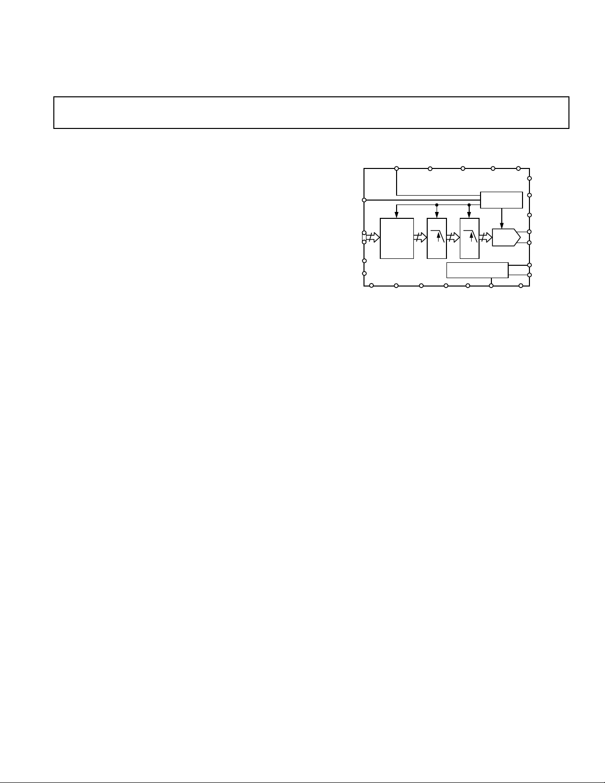
FUNCTIONAL DESCRIPTION
Figure 22 shows a simplified block diagram of the AD9774. The
AD9774 is a complete, 4× oversampling, 14-bit DAC that includes two cascaded 2× interpolation filters, a phase-locked loop
(PLL) clock multiplier, and a 1.20 Volt bandgap voltage reference. The 14-bit DAC provides two complementary current
outputs whose full-scale current is determined by an external
resistor. Input data that is latched into the edge-triggered input
latches is first interpolated by a factor of four by the interpolation
filters before updating the 14-bit DAC. A PLL clock multiplier
produces the necessary internally synchronized 1×, 2× and 4×
clocks from an external reference. The AD9774 can support
input data rates as high as 32 MSPS, corresponding to a DAC
update rate of 128 MSPS.
The analog and digital sections of the AD9774 have separate
power supply inputs (i.e., AVDD and DVDD) that can operate
over a 2.7 V to 5.5 V range. A separate supply input (i.e.,
PLLVDD) having a similar operating range is also provided for
the PLL clock multiplier. To maintain optimum noise and distortion performance, PLLVDD should be maintained at the
same voltage level as DVDD.
PLL
VCO
CLK IN/OUT
DATA
INPUTS
(DB13–DB0)
SNOOZE
SLEEP
14
DCOM
CLK43IN
TRIGGERED
LATCHES
DVDD
PLLLOCK
13 23 43
14
EDGE
23
ICOMP ACOM AVDD
PLL
ENABLE
AD9774
14
23
+1.2V REFERENCE
AND CONTROL AMP
REFCOMP REFLO
DIVIDE
IN/EXT
PLL CLOCK
MULTIPLIER
43
14
14-BIT
DAC
PLLCOM
LPF
PLLVDD
IOUTA
IOUTB
REFIO
FSADJ
Figure 22. Functional Block Diagram
Preceding the 14-bit DAC are two cascaded 2× digital interpola-
tion filter stages based on a 55- and 23-tap halfband symmetric
FIR topology. Edge triggered latches are used to latch the input
data on the rising edge of CLK IN/OUT. The composite frequency and impulse response of both filters are shown in Figures 2a and 2b. Table I and Table II list the idealized filter
coefficients for each of the filter stages. The interpolation filters
essentially multiply the input data rate to the DAC by a factor of
four relative to its original input data rate while simultaneously
reducing the magnitude of the images associated with the original input data rate.
The benefits of an interpolation filter are clearly seen in Figure
23, which shows an example of the frequency and time domain
representation of a discrete time sine wave signal before and
after it is applied to a digital interpolation filter. Images of the
sine wave signal appear around multiples of the DAC’s input
data rate as predicted by sampling theory. These undesirable
images will also appear at the output of a reconstruction DAC,
although modified by the DAC’s sin(x)/(x) roll-off response.
In many bandlimited applications, these images must be suppressed by an analog filter following the DAC. The complexity
of this analog filter is typically determined by the proximity of
the desired fundamental to the first image and the required
amount of image suppression. Adding to the complexity of this
analog filter may be the requirement of compensating for the
DAC’s sin(x)/x response.
Referring to Figure 23, the “new” first image associated with the
DAC’s higher data rate after interpolation is “pushed” out further relative to the input signal. The “old” first image associated
with the lower DAC data rate before interpolation is suppressed
by the digital filter. As a result, the transition band for the analog reconstruction filter is increased, thus reducing the complexity of the analog filter. Furthermore, the sin(x)/x roll-off over the
effective passband (i.e., dc to f
/2) is significantly reduced.
CLOCK
The AD9774 includes a PLL clock multiplier that produces the
necessary internally synchronized 1×, 2× and 4× clocks for the
edge triggered latches, interpolation filters and DACs. The
PLL clock multiplier typically accepts an input data clock,
CLK IN/OUT, as its reference source. Alternatively, it can also
be configured using an external 4× clock via CLK4×IN. The
PLLDIVIDE, VCO IN/EXT, PLLENABLE, and PLLLOCK
are control inputs/outputs used in the PLL clock generator.
Refer to the PLL CLOCK MULTIPLIER OPERATION section for a detailed discussion on its operation.
The digital section of the AD9774 also includes several other
control inputs and outputs. The SLEEP and SNOOZE inputs
provide different power-saving modes as discussed in the
SLEEP and SNOOZE section.
1
4
f
4f
CLOCK
"NEW"
1ST IMAGE
CLOCK
TIME DOMAIN
FUNDAMENTAL
FREQUENCY DOMAIN
1
f
CLOCK
1ST IMAGE
2f
CLOCK
INPUT DATA LATCH
f
CLOCK
4f
CLOCK
FUNDAMENTAL
DIGITAL
SUPPRESSED
"OLD"
1ST IMAGE
4x INTERPOLATION FILTER
FILTER
2f
43f
CLOCK
4x
CLOCK
Figure 23. Time and Frequency Domain Example of Digital Interpolation Filter
–10–
2f
DAC
CLOCK
DACs
4f
"SINX"
X
CLOCK
REV. B

AD9774
PLL CLOCK MULTIPLIER OPERATION
The Phase Lock Loop (PLL) Clock Multiplier is intrinsic to the
operation of the AD9774 in that it produces the necessary inter-
nally synchronized 1×, 2× and 4× clocks for the edge triggered
latches, interpolation filters and DACs. Figure 24 shows a functional block diagram of the PLL Clock Multiplier, which consists of a phase detector, a charge pump, a voltage controlled
oscillator (VCO), a divide-by-N circuit and some control inputs/
outputs. It produces the required internal clocks for the AD9774
by using one of two possible externally applied reference clock
sources applied to either CLKIN or CLK4×IN. PLLENABLE
and VCO IN/EXT are active HIGH control inputs used to
enable the charge pump and VCO respectively.
To maintain optimum noise and distortion performance,
PLLVDD and DVDD should be set to similar voltage levels. If
a separate supply cannot be provided for PLLVDD, PLLVDD
can be tied to DVDD using an LC filter network similar to that
shown in Figure 41.
Many applications will select a reference clock operating at the
data input rate as shown in Figure 24. In this case, the external
clock source is applied to CLKIN and the PLL Clock Multiplier
is fully enabled by tying PLLENABLE and VCO IN/EXT to
PLLVDD. Note, CLKIN must adhere to the timing require-
ments shown in Figure 1. A 1.5 kΩ resistor and 0.01 µF ceramic
capacitor connected in series from LPF to PLLVDD are required to optimize the phase noise vs. settling/acquisition time
characteristics of the PLL. PLLLOCK is a control output, active HIGH, which may be monitored upon system power-up to
indicate that the PLL is successfully “locked” to CLKIN. Note,
applications employing multiple AD9774 devices will benefit
from the PLL Clock Multiplier’s ability to ensure precise simultaneous updating/phase synchronization of these devices when
driven by the same input clock source.
PLLDIVIDE is used to preset the “lock-in” range of the PLL. It
should be tied to PLLCOM if CLKIN is greater than 10 MHz
and to PLLVDD if CLKIN is between 5.5 MHz and 10 MHz.
For operation below 5.5 MHz (i.e., input data rates less than
5.5 MSPS), the internal charge pump and VCO should be
disabled by tying PLLENABLE and VCO IN/EXT LOW. In
this case, the user MUST supply a system clock operating at 4×
the input data rate as discussed below.
CONNECT TO
PLLCOM
PLL
DIVIDE
CLK
IN/OUT
PHASE
DETECTOR
48
44
DIVIDE-
BY-N
42
41
DCOM
+2.7 TO +5.5 V
DVDD
PLLLOCK
AD9774
CLK
43IN
D
CONNECT TO
PLLVDD
PLL
ENABLE
CHARGE
PUMP
VCO
VCO
VCO
IN/EXT
LPF
PLL
VDD
PLL
COM
1.5kV
0.01mF
+2.7 TO
+5.5 V
D
Figure 24. Clock Multiplier with PLL Enabled
There are two cases in which a user may consider or be required
to disable the internal PLL Clock Multiplier and supply the
AD9774 with an external 4× system clock. Applications already
containing a system clock operating at four (i.e., 4×) the input
data rate may consider using it as the master clock source. Applications with input data rates less than 5.5 MSPS must use a
master 4× clock.
In any of these cases, the clock source is applied to CLK4×IN
and the PLL is partially disabled by typing PLLENABLE and
VCO IN/EXT to PLLCOM as shown in Figure 25. LPF may
remain open since this portion of the PLL circuitry is disabled.
The divide-by-N circuit still remains enabled providing a 1× or
2× internal clock at CLOCK IN/OUT depending on the state of
PLLDIVIDE. Since the digital input data is latched into the
AD9774 on the rising edge of the 1× clock, PLLDIVIDE should
be tied to PLLCOM such that the 1× clock appears as an output
at CLOCK IN/OUT. The input data should be stable 5 ns (i.e.,
data set-up) before the rising edge of the 1× clock appearing at
CLOCK IN/OUT and remain stable for 1 ns after the rising
edge (i.e., data hold) to ensure proper latching. Note, the rising
edge of the 1× clock occurs approximately 9 ns to 15 ns relative
to the falling edge of the CLK4× input. If a data timing issue
exists between the AD9774 and its external driver device, the
CLK4× input can be inverted via an external gate to ensure
proper set-up and hold time.
PLLLOCK
PLL
DIVIDE
CLK
IN/OUT
DETECTOR
48
44
DIVIDE-
BY-N
42
41
DCOM
+2.7 TO +5.5 V
PHASE
DVDD
AD9774
CLK
43IN
D
PLL
ENABLE
CHARGE
PUMP
VCO
VCO
VCO
IN/EXT
PLL
VDD
LPF
PLL
COM
+2.7 TO +5.5 V
D
Figure 25. Clock Divider with PLL Disabled
DAC OPERATION
The 14-bit DAC along with the 1.2 V reference and reference
control amplifier is shown in Figure 26. The DAC consists of a
large PMOS current source array capable of providing up to
20 mA of full-scale current, I
. The array is divided into 31
OUTFS
equal currents which make up the five most significant bits
(MSBs). The next four bits or middle bits consist of 15 equal
current sources whose values are 1/16th of an MSB current
source. The remaining LSBs are binary weighted fractions of the
middle-bits current sources. All of these current sources are
switched to one or the other of two output nodes (i.e., IOUTA
or IOUTB) via PMOS differential current switches. Implementing the middle and lower bits with current sources, instead of an
R-2R ladder, enhances its dynamic performance for multitone
or low amplitude signals and helps maintain the DAC’s high
output impedance (i.e., > 100 kΩ).
–11–REV. B

AD9774
1.91kV
0.1mF
0.1mF
REFLO AVDD
1.20V REF
REFIO
FS ADJ
AD9774
REFCOMP
50pF
SEGMENTED
SWITCHES
+2.7 TO +5.5V
CURRENT
SOURCE
ARRAY
ACOM
LSB
SWITCHES
A
ICOMP
0.1mF
IOUTA
IOUTB
Figure 26. Block Diagram of Internal DAC, 1.2 V Reference,
and Reference Control Circuits
The full-scale output current is regulated by the reference control amplifier and can be set from 2 mA to 20 mA via an external resistor, R
. The external resistor,␣ in combination with
SET
both the reference control amplifier and voltage reference,
REFIO, sets the reference current, I
, which is mirrored over
REF
to the segmented current sources with the proper scaling factor.
The full-scale current, I
value of I
REF
.
, is exactly thirty-two times the
OUTFS
DAC TRANSFER FUNCTION
The AD9774 provides complementary current outputs, IOUTA
and IOUTB. IOUTA will provide a near full-scale current output, I
, when all bits are high (i.e., DAC CODE = 16383)
OUTFS
while IOUTB, the complementary output, provides no current.
The current output appearing at IOUTA and IOUTB is a function of both the input code and I
IOUTA = (DAC CODE/16384) × I
IOUTB = (16383 – DAC CODE)/16384 × I
and can be expressed as:
OUTFS
OUTFS
OUTFS
(1)
(2)
where DAC CODE = 0 to 16383 (i.e., Decimal Representation).
As previously mentioned, I
current I
V
REFIO
I
where I
, which is nominally set by a reference voltage
REF
and external resistor R
= 32 × I
OUTFS
REF
= V
REF
REFIO/RSET
is a function of the reference
OUTFS
. It can be expressed as:
SET
(3)
(4)
The two current outputs will typically drive a resistive load
directly or via a transformer. If dc coupling is required, IOUTA
and IOUTB should be directly connected to matching resistive
loads, R
that R
, that are tied to analog common, ACOM. Note
LOAD
may represent the equivalent load resistance seen by
LOAD
IOUTA or IOUTB as would be the case in a doubly terminated
50 Ω or 75 Ω cable. The single-ended voltage output appearing
at the IOUTA and IOUTB nodes is simply:
V
= IOUTA × R
OUTA
V
= IOUTB × R
OUTB
Note that the full-scale value of V
LOAD
LOAD
OUTA
and V
should not
OUTB
(5)
(6)
exceed the specified output compliance range to maintain specified distortion and linearity performance.
The differential voltage, V
, appearing across IOUTA and
DIFF
IOUTB is:
V
= (IOUTA – IOUTB) × R
DIFF
LOAD
(7)
Substituting the values of IOUTA, IOUTB and I
REF
; V
DIFF
can
be expressed as:
V
= {(2 DAC CODE – 16383)/16384} ×
DIFF
V
= {(32 R
DIFF
LOAD/RSET
) × V
REFIO
(8)
These last two equations highlight some of the advantages of
operating the AD9774 differentially. First, the differential
operation will help cancel common-mode error sources associated with IOUTA and IOUTB such as noise, distortion and dc
offsets. Second, the differential code-dependent current and
subsequent voltage, V
voltage output (i.e., V
, is twice the value of the single-ended
DIFF
OUTA
or V
), thus providing twice the
OUTB
signal power to the load.
Note that the gain drift temperature performance for a singleended (VOUTA and VOUTB) or differential output (V
DIFF
) of
the AD9774 can be enhanced by selecting temperature tracking
resistors for R
LOAD
and R
due to their ratiometric relation-
SET
ship as shown in Equation 8.
REFERENCE OPERATION
The AD9774 contains an internal 1.20 V bandgap reference
that can be easily disabled and overridden by an external
reference. REFIO serves as either an input or output, depending
on whether the internal or external reference is selected. If
REFLO is tied to ACOM, as shown in Figure 27, the internal
reference is activated, and REFIO provides a 1.20 V output. In
this case, the internal reference must be compensated externally
with a ceramic chip capacitor of 0.1 µF or greater from REFIO
to REFLO. If any additional loading is required, REFIO should
be buffered with an external amplifier having an input bias current less than 100 nA.
ADDITIONAL
LOAD
OPTIONAL
EXTERNAL
REF BUFFER
0.1mF
2kV
REFLO
+1.2V REF
REFIO
FSADJ
AD9774
+2.7 TO +5.5V
0.1mF
REFCOMP
50pF
CURRENT
AVDD
SOURCE
ARRAY
A
Figure 27. Internal Reference Configuration
The internal reference can be disabled by connecting REFLO to
AVDD. In this case, an external reference may then be applied
to REFIO as shown in Figure 28. The external reference may
provide either a fixed reference voltage to enhance accuracy and
drift performance or a varying reference voltage for gain control.
Note that the 0.1 µF compensation capacitor is not required
since the internal reference is disabled, and the high input im-
pedance (i.e., 1 MΩ) of REFIO minimizes any loading of the
external reference.
–12–
REV. B

AD9774
AVDD
EXTERNAL
REF
+2.7 TO +5.5V
0.1mF
REFCOMP
+1.2V REF
V
REFIO
R
I
SET
REF
V
REFIO/RSET
REFIO
FS ADJ
=
AD9774
50pF
REFERENCE
CONTROL
AMPLIFIER
CURRENT
SOURCE
A
AVDDREFLO
ARRAY
Figure 28. External Reference Configuration
REFERENCE CONTROL AMPLIFIER
The AD9774 also contains an internal control amplifier that is
used to regulate the DAC’s full-scale output current, I
OUTFS
.
The control amplifier is configured as a V-I converter, as shown
in Figure 28, such that its current output, I
the ratio of the V
in Equation 4. I
and an external resistor, R
REFIO
is copied over to the segmented current
REF
sources with the proper scaling factor to set I
, is determined by
REF
SET
OUTFS
, as stated
as stated in
Equation 3.
The control amplifier allows a wide (10:1) adjustment span of
I
over a 2 mA to 20 mA range by setting I
OUTFS
62.5 µA and 625 µA. The wide adjustment span of I
between
REF
OUTFS
provides several application benefits. The first benefit relates
directly to the power dissipation of the AD9774, which is proportional to I
(refer to the Power Dissipation section). The
OUTFS
second benefit relates to the 20 dB adjustment, which is useful
for system gain control purposes.
There are two methods by which I
R
. The first method is suitable for a single-supply system in
SET
can be varied for a fixed
REF
which the internal reference is disabled, and the common-mode
voltage of REFIO is varied over its compliance range of 1.25 V
to 0.10 V. REFIO can be driven by a single-supply amplifier or
DAC, thus allowing I
to be varied for a fixed R
REF
. Since the
SET
input impedance of REFIO is approximately 1 MΩ, a simple,
low cost R-2R ladder DAC configured in the voltage mode
topology may be used to control the gain. This circuit is shown
in Figure 30 using the AD7524 and an external 1.2 V reference,
the AD1580.
The second method may be used in a dual-supply system in
which the common-mode voltage of REFIO is fixed, and I
REF
is
varied by an external voltage, V
, applied to R
GC
via an ampli-
SET
fier. An example of this method is shown in Figure 29 in which
the internal reference is used to set the common-mode voltage
of the control amplifier to 1.20 V. The external voltage, V
GC
, is
referenced to ACOM and should not exceed 1.2 V. The value of
R
is such that I
SET
REFMAX
and I
do not exceed 62.5 µA
REFMIN
and 625 µA, respectively. The associated equations in Figure 29
can be used to determine the value of R
+1.2V REF
REFIO
I
REF
I
REF
WITH V
FSADJ
AD9774
= (1.2–VGC)/R
, V
GC
REFIO
V
1mF
GC
R
SET
.
SET
REFCOMP
50pF
SET
AND 62.5 mA # I
+2.7 TO +5.5V
0.1mF
AVDDREFLO
CURRENT
SOURCE
ARRAY
# 625A
REF
A
Figure 29. Dual Supply Gain Control Circuit
ANALOG OUTPUTS
The AD9774 produces two complementary current outputs,
IOUTA and IOUTB, which may be configured for single-end or
differential operation. IOUTA and IOUTB can be converted
into complementary single-ended voltage outputs, V
, via a load resistor, R
V
OUTB
, as described in the DAC
LOAD
OUTA
and
Transfer Function section by Equations 5 through 8. The
differential voltage, V
, existing between V
DIFF
OUTA
and V
OUTB
,
can also be converted to a single-ended voltage via a transformer
or differential amplifier configuration.
Figure 31 shows the equivalent analog output circuit of the
AD9774 consisting of a parallel combination of PMOS differential current switches associated with each segmented current
source. The output impedance of IOUTA and IOUTB is determined by the equivalent parallel combination of the PMOS
switches and is typically 100 kΩ in parallel with 5 pF. Due to
the nature of a PMOS device, the output impedance is also
slightly dependent on the output voltage (i.e., V
OUTA
and V
OUTB
)
and, to a lesser extent, the analog supply voltage, AVDD, and
full-scale current, I
. Although the output impedance’s
OUTFS
signal dependency can be a source of dc nonlinearity and ac linearity (i.e., distortion), its effects can be limited if certain precautions are noted.
1.2V
AD1580
AVDD
OUT1
OUT2
R
FB
AD7524
AGND
V
DD
V
DB7–DB0
REF
0.1V TO 1.2V
R
SET
I
REF
V
REF/RSET
REFLO
+1.2V REF
REFIO
FSADJ
=
AD9774
REFCOMP
Figure 30. Single Supply Gain Control Circuit
–13–REV. B
50pF
+2.7 TO +5.5V
0.1mF
AVDD
CURRENT
SOURCE
ARRAY
A

AD9774
AD9774
AVDD
IOUTA
R
LOAD
Figure 31. Equivalent Analog Output Circuit
IOUTA and IOUTB also have a negative and positive voltage
compliance range. The negative output compliance range of
–1.0 V is set by the breakdown limits of the CMOS process.
Operation beyond this maximum limit may result in a breakdown of the output stage and affect the reliability of the AD9774.
The positive output compliance range is slightly dependent on
the full-scale output current, I
nominal 1.25 V for an I
= 20 mA to 1.00 V for an I
OUTFS
. It degrades slightly from its
OUTFS
2 mA. Operation beyond the positive compliance range will
induce clipping of the output signal, which severely degrades
the AD9774’s linearity and distortion performance.
For applications requiring the optimum dc linearity, IOUTA
and/or IOUTB should be maintained at a virtual ground via an
I-V op amp configuration. Maintaining IOUTA and/or IOUTB
at a virtual ground keeps the output impedance of the AD9774
fixed, significantly reducing its effect on linearity. However, it
does not necessarily lead to the optimum distortion performance due to limitations of the I-V op amp. Note that the
INL/DNL specifications for the AD9774 are measured in this
manner using IOUTA. In addition, these dc linearity specifications remain virtually unaffected over the specified power
supply range of 2.7 V to 5.5 V.
Operating the AD9774 with reduced voltage output swings at
IOUTA and IOUTB in a differential or single-ended output
configuration reduces the signal dependency of its output impedance thus enhancing distortion performance. Although the
voltage compliance range of IOUTA and IOUTB extends from
–1.0 V to +1.25 V, optimum distortion performance is achieved
when the maximum full-scale signal at IOUTA and IOUTB
does not exceed approximately 0.5 V. A properly selected transformer with a grounded center-tap will allow the AD9774 to
provide the required power and voltage levels to different loads
while maintaining reduced voltage swings at IOUTA and
IOUTB. DC-coupled applications requiring a differential or
single-ended output configuration should size R
ingly. Refer to Applying the AD9774 section for examples of
various output configurations.
The most significant improvement in the AD9774’s distortion
and noise performance is realized using a differential output
configuration. The common-mode error sources of both IOUTA
and IOUTB can be substantially reduced by the common-mode
rejection of a transformer or differential amplifier. These
common-mode error sources include even-order distortion
products and noise. The enhancement in distortion performance
becomes more significant as the reconstructed waveform’s
frequency content increases and/or its amplitude decreases.
IOUTB
R
LOAD
LOAD
OUTFS
accord-
=
–14–
The distortion and noise performance of the AD9774 is also
slightly dependent on the analog and digital supply as well as the
full-scale current setting, I
. Operating the analog supply at
OUTFS
5.0 V ensures maximum headroom for its internal PMOS current
sources and differential switches leading to improved distortion
performance. Although I
20 mA, selecting an I
OUTFS
can be set between 2 mA and
OUTFS
of 20 mA will provide the best distortion and noise performance. The noise performance of the
AD9774 is affected by the digital supply (DVDD), output frequency, and increases with increasing clock rate. Operating the
AD9774 with low voltage logic levels between 3 V and 3.3 V
will slightly reduce the amount of on-chip digital noise.
In summary, the AD9774 achieves the optimum distortion and
noise performance under the following conditions:
(1) Differential Operation.
(2) Positive voltage swing at IOUTA and IOUTB limited to
+0.5 V.
(3) IOUTFS set to 20 mA.
(4) Analog Supply (AVDD) set at 5.0 V.
(5) Digital Supply (DVDD) and Phase Lock Loop Supply
(PLLVDD) set at 3.0 V to 3.3 V with appropriate logic
levels.
Note that the ac performance of the AD9774 is characterized
under the above-mentioned operating conditions.
DIGITAL INPUTS/OUTPUTS
The digital input of the AD9774 consists of 14 data input pins
and a clock input pin, and several control input pins. Since
some of the internal logic is operated from DVDD and PLLVDD,
they must be set to the same or similar levels to ensure proper
compatibility with any external logic/drivers. The two digital
outputs of the AD9774, PLL LOCK and CLK OUT originate
from the internal PLL circuitry and thus its output logic levels
will be set by PLLVDD.
The 14-bit parallel data inputs follow standard positive binary
coding where DB13 is the most significant bit (MSB), and DB0
is the least significant bit (LSB). IOUTA produces a full-scale
output current when all data bits are at Logic 1. IOUTB produces a complementary output with the full-scale current split
between the two outputs as a function of the input code.
The digital interface is implemented using an edge-triggered
master slave latch and is designed to support a clock and input
data rate as high as 32 MSPS. The clock can be operated at any
duty cycle that meets the specified latch pulsewidth as shown in
Figure 1. The setup and hold times can also be varied within the
clock cycle as long as the specified minimum times are met.
The digital inputs are CMOS-compatible with logic thresholds,
V
THRESHOLD,
set to approximately half the digital positive supply
(i.e., DVDD or PLLVDD) or
V
THRESHOLD
= DVDD/2 (±20%)
The internal digital circuitry of the AD9774 is capable of operating
over a digital supply range of 2.7 V to 5.5 V. As a result, the
digital inputs can also accommodate TTL levels when DVDD is
set to accommodate the maximum high level voltage of the TTL
drivers V
OH(MAX)
. A DVDD of 3 V to 3.3 V will typically ensure
proper compatibility with most TTL logic families. Figure 32
shows the equivalent digital input circuit for the data and clock
inputs.
REV. B

AD9774
I
OUTFS
– mA
30
0
2204 6 8 1012141618
25
20
15
10
5
I
AVDD
– mA
RATIO –
f
OUT
/
f
CLOCK
200
180
20
0.01
1.00.10
I
DVDD
– mA
100
80
60
40
140
120
160
0
32MSPS
16MSPS
8MSPS
4MSPS
DVDD
DIGITAL
INPUT
Figure 32. Equivalent Digital Input
Since the AD9774 is capable of being updated up to 32 MSPS,
the quality of the clock and data input signals are important in
achieving the optimum performance. Operating the AD9774
with reduced logic swings and a corresponding digital supply
(DVDD) will result in the lowest data feedthrough and on-chip
digital noise. The drivers of the digital data interface circuitry
should be specified to meet the minimum setup and hold times
of the AD9774 as well as its required min/max input logic level
thresholds.
Digital signal paths should be kept short and run lengths matched
to avoid propagation delay mismatch. The insertion of a low
value resistor network (i.e., 20 Ω to 100 Ω) between the AD9774
digital inputs and driver outputs may be helpful in reducing any
overshooting and ringing at the digital inputs that contribute to
data feedthrough.
The external clock driver circuitry should provide the AD9774
with a low jitter clock input meeting the min/max logic levels
while providing fast edges. Fast clock edges will help minimize
any jitter that will manifest itself as phase noise on a reconstructed waveform. Thus, the clock input should be driven by
the fastest logic family suitable for the application.
DVDD = 3 V, respectively. Note, how I
is reduced by more
DVDD
than a factor of 2 when DVDD is reduced from 5 V to 3 V.
Figure 33. I
AVDD
vs. I
OUTFS
SLEEP AND SNOOZE MODE OPERATION
The AD9774 has a SLEEP function that turns off the output
current and reduces the supply current to less than 5 mA over
the specified supply range of 2.7 V to 5.5 V and temperature
range. This mode can be activated by applying a logic level “1”
to the SLEEP pin. The AD9774 takes less than 0.1 µs to power
down and approximately 6.4 µs to power back up.
The SNOOZE mode should be considered as an alternative
power-savings option if the power-up characteristics of the
SLEEP mode are unsuitable. This mode, which is also activated
by applying a logic level “1” to the SNOOZE pin, disables the
AD9774’s digital filters only, resulting in significant power
savings. Both the SLEEP and SNOOZE pins should be tied to
DCOM if power savings is not required.
POWER DISSIPATION
The power dissipation, PD, of the AD9774 is dependent on
several factors, including: (1) AVDD, PLLVDD, and DVDD,
the power supply voltages; (2) I
output; (3) f
digital input waveform. The power dissipation is directly pro-
, the update rate; and (4) the reconstructed
CLOCK
portional to the analog supply current, I
supply current, I
DVDD
. I
AVDD
as shown in Figure 33, and is insensitive to f
Conversely, I
form, f
CLOCK
show I
DVDD
(f
OUT/fCLOCK
is dependent on both the digital input wave-
DVDD
, and digital supply DVDD. Figures 34 and 35
as a function of full-scale sine wave output ratios
) for various update rates with DVDD = 5 V and
, the full-scale current
OUTFS
, and the digital
is directly proportional to I
AVDD
OUTFS,
.
CLOCK
Figure 34. I
100
90
80
70
60
– mA
50
DVDD
40
I
30
20
10
0
0.01
Figure 35. I
vs. Ratio @ DVDD = 5 V
DVDD
32MSPS
16MSPS
8MSPS
4MSPS
RATIO –
f
/
f
OUT
CLOCK
vs. Ratio @ DVDD = 3 V
DVDD
1.00.10
For those applications requiring the AD9774 to operate under the
following conditions: (1) AVDD, PLLVDD and DVDD = +5 V;
(2) f
> 25 MSPS; and (3) ambient temperatures > 70°C;
CLOCK
proper thermal management via a heatsink or thermal epoxy is
recommended.
–15–REV. B

AD9774
APPLYING THE AD9774
OUTPUT CONFIGURATIONS
The following sections illustrate some typical output configurations for the AD9774. Unless otherwise noted, it is assumed
that I
ing the optimum dynamic performance, a differential output
configuration is suggested. A differential output configuration
may consist of either an RF transformer or a differential op amp
configuration. The transformer configuration provides the optimum high frequency performance and is recommended for any
application allowing for ac coupling. The differential op amp
configuration is suitable for applications requiring dc coupling, a
bipolar output, signal gain and/or level shifting.
A single-ended output is suitable for applications requiring a
unipolar voltage output. A positive unipolar output voltage will
result if IOUTA and/or IOUTB is connected to an approximately
sized load resistor, R
tion may be more suitable for a single-supply system requiring a
dc-coupled, ground referred output voltage. Alternatively, an
amplifier could be configured as an I-V converter, thus converting IOUTA or IOUTB into a negative unipolar voltage. This
configuration provides the best dc linearity since IOUTA or
IOUTB is maintained at a virtual ground.
DIFFERENTIAL COUPLING USING A TRANSFORMER
An RF transformer can be used to perform a differential-tosingle-ended signal conversion as shown in Figure 36. A
differentially coupled transformer output provides the optimum
distortion performance for output signals whose spectral content
lies within the transformer’s passband. An RF transformer such
as the Mini-Circuits T1-1T provides excellent rejection of
common-mode distortion (i.e., even-order harmonics) and noise
over a wide frequency range. It also provides electrical isolation
and the ability to deliver twice the power to the load. Transformers with different impedance ratios may also be used for
impedance matching purposes. Note that the transformer
provides ac coupling only.
The center tap on the primary side of the transformer must be
connected to ACOM to provide the necessary dc current path
for both IOUTA and IOUTB. The complementary voltages
appearing at IOUTA and IOUTB (i.e., V
swing symmetrically around ACOM and should be maintained
with the specified output compliance range of the AD9774. A
differential resistor, R
which the output of the transformer is connected to the load,
R
LOAD
mined by the transformer’s impedance ratio and provides the
proper source termination that results in a low VSWR. Note that
approximately half the signal power will be dissipated across R
is set to a nominal 20 mA. For applications requir-
OUTFS
, referred to ACOM. This configura-
LOAD
MINI-CIRCUITS
IOUTA
AD9774
IOUTB
22
21
T1-1T
OPTIONAL R
DIFF
R
LOAD
Figure 36. Differential Output Using a Transformer
and V
OUTA
, may be inserted in applications in
DIFF
, via a passive reconstruction filter or cable. R
OUTB
DIFF
)
is deter-
DIFF
.
DIFFERENTIAL USING AN OP AMP
An op amp can also be used to perform a differential-to-singleended conversion as shown in Figure 37. The AD9774 is
configured with two equal load resistors, R
, of 25 Ω. The
LOAD
differential voltage developed across IOUTA and IOUTB is
converted to a single-ended signal via the differential op amp
configuration. An optional capacitor can be installed across
IOUTA and IOUTB, forming a real pole in a low-pass filter.
The addition of this capacitor also enhances the op amp’s distortion performance by preventing the DAC’s high slewing output
from overloading the op amp’s input.
500V
AD9774
IOUTA
IOUTB
22
21
C
OPT
225V
225V
25V25V
AD8055
500V
Figure 37. DC Differential Coupling Using an Op Amp
The common-mode rejection of this configuration is typically
determined by the resistor matching. In this circuit, the differential op amp circuit using the AD8055 is configured to provide
some additional signal gain. The op amp must operate from a
dual supply since its output is approximately ±1.0 V. A high
speed amplifier capable of preserving the differential performance of the AD9774 while meeting other system level objectives
(i.e., cost, power) should be selected. The op amps differential
gain, its gain setting resistor values and full-scale output swing
capabilities should all be considered when optimizing this circuit.
The differential circuit shown in Figure 38 provides the necessary level-shifting required in a single supply system. In this case,
AVDD, which is the positive analog supply for both the AD9774
and the op amp, is also used to level-shift the differential output
of the AD9774 to midsupply (i.e., AVDD/2). The AD8041 is a
suitable op amp for this application.
500
AD9774
IOUTA
IOUTB
22
21
C
OPT
225
1k
AD8041
1k
AVDD
225
2525
Figure 38. Single-Supply DC Differential Coupled Circuit
SINGLE-ENDED UNBUFFERED VOLTAGE OUTPUT
Figure 39 shows the AD9774 configured to provide a unipolar
output range of approximately 0 V to +0.5 V for a doubly termi-
nated 50 Ω cable since the nominal full-scale current, I
20 mA flows through the equivalent R
represents the equivalent load resistance seen by IOUTA.
R
LOAD
of 25 Ω. In this case,
LOAD
OUTFS
, of
The unused output (IOUTB) can be connected to ACOM directly. Different values of I
OUTFS
and R
can be selected as
LOAD
–16–
REV. B

AD9774
long as the positive compliance range is adhered to. One additional consideration in this mode is the integral nonlinearity
(INL) as discussed in the Analog Output section of this data
sheet. For optimum INL performance, the single-ended, buffered voltage output configuration is suggested.
AD9774
IOUTA
IOUTB
I
= 20mA
OUTFS
22
50V 50V
21
V
OUTA
= 0 TO +0.5V
Figure 39. 0 V to +0.5 V Unbuffered Voltage Output
SINGLE-ENDED BUFFERED VOLTAGE OUTPUT
CONFIGURATION
Figure 40 shows a buffered single-ended output configuration in
which the op amp U1 performs an I-V conversion on the AD9774
output current. U1 maintains IOUTA (or IOUTB) at a virtual
ground, thus minimizing the nonlinear output impedance effect
on the DAC’s INL performance as discussed in the Analog
Output section. Although this single-ended configuration typically provides the best dc linearity performance, its ac distortion
performance at higher DAC update rates may be limited by
U1’s slewing capabilities. U1 provides a negative unipolar output
voltage and its full-scale output voltage is simply the product of
and I
R
FB
voltage output swing capabilities by scaling I
. The full-scale output should be set within U1’s
OUTFS
OUTFS
and/or RFB.
An improvement in ac distortion performance may result with a
reduced I
since the signal current U1 will be required to
OUTFS
sink will be subsequently reduced.
C
OPT
R
FB
200V
U1
V
= I
OUTFS
3 R
FB
OUT
AD9774
IOUTA
IOUTB
I
= 10mA
OUTFS
22
21
200V
Figure 40. Unipolar Buffered Voltage Output
POWER AND GROUNDING CONSIDERATIONS
In systems seeking to simultaneously achieve high speed and
high performance, the implementation and construction of the
printed circuit board design is often as important as the circuit
design. Proper RF techniques must be used in device selection,
placement and routing and supply bypassing and grounding.
Figures 44–49 illustrate the recommended printed circuit board
ground, power and signal plane layouts that are implemented on
the AD9774 evaluation board.
Proper grounding and decoupling should be a primary objective
in any high speed, high resolution system. The AD9774 features
separate analog and digital supply and ground pins to optimize
the management of analog and digital ground currents in a
system. In general, AVDD, the analog supply, should be decoupled
to ACOM, the analog common, as close to the chip as physically possible. Similarly, DVDD, the digital supply, should be
decoupled to DCOM and PLLVDD, the Phase Lock Loop
Supply, should be decoupled to PLLCOM.
For those applications requiring a single +5 V or +3 V supply
for both the analog, digital supply and Phase Lock Loop supply,
a clean AVDD and/or PLLVDD may be generated using the
circuit shown in Figure 41. The circuit consists of a differential
LC filter with separate power supply and return lines. Lower
noise can be attained using low ESR type electrolytic and tantalum capacitors.
FERRITE
TTL/CMOS
LOGIC
CIRCUITS
+5V OR +3V
POWER SUPPLY
BEADS
100mF
ELECT.
10-22mF
TANT.
0.1mF
CER.
AVDD
ACOM
Figure 41. Differential LC Filter for Single +5 V or +3 V
Applications
Maintaining low noise on power supplies and ground is critical
to obtain optimum results from the AD9774. If properly
implemented, ground planes can perform a host of functions on
high speed circuit boards: bypassing, shielding current transport, etc. In mixed signal design, the analog and digital portions
of the board should be distinct from each other, with the analog
ground plane confined to the areas covering the analog signal
traces, and the digital ground plane confined to areas covering
the digital interconnects.
All analog ground pins of the DAC, reference and other analog
components should be tied directly to the analog ground plane.
The two ground planes should be connected by a path 1/8 to
1/4 inch wide underneath or within 1/2 inch of the DAC to
maintain optimum performance. Care should be taken to ensure
that the ground plane is uninterrupted over crucial signal paths.
On the digital side, this includes the digital input lines running
to the DAC as well as any clock signals. On the analog side, this
includes the DAC output signal, reference signal and the supply
feeders.
The use of wide runs or planes in the routing of power lines is
also recommended. This serves the dual role of providing a low
series impedance power supply to the part, as well as providing
some “free” capacitive decoupling to the appropriate ground
plane. It is essential that care be taken in the layout of signal and
power ground interconnects to avoid inducing extraneous voltage drops in the signal ground paths. It is recommended that all
connections be short, direct and as physically close to the package as possible in order to minimize the sharing of conduction
paths between different currents. When runs exceed an inch in
length, strip line techniques with proper termination resistors
should be considered. The necessity and value of this resistor
will be dependent upon the logic family used.
For a more detailed discussion of the implementation and construction of high speed, mixed signal printed circuit boards,
refer to Analog Devices’ application notes AN-280 and AN-333.
–17–REV. B

AD9774
MULTITONE PERFORMANCE CONSIDERATIONS AND
CHARACTERIZATION
The frequency domain performance of high speed DACs has
traditionally been characterized by analyzing the spectral output
of a reconstructed full-scale (i.e., 0 dBFS), single-tone sine wave
at a particular output frequency and update rate. Although this
characterization data is useful, it is often insufficient to reflect a
DAC’s performance for a reconstructed multitone or spreadspectrum waveform. In fact, evaluating a DAC’s spectral
performance using a full-scale, single tone at the highest specified
frequency (i.e., f
) of a bandlimited waveform is typically
H
indicative of a DAC’s “worst-case” performance for that given
waveform. In the time domain, this full-scale sine wave represents the lowest peak-to-rms ratio or crest factor (i.e., V
PEAK
/
V rms) that this bandlimited signal will encounter.
0
–10
–20
–30
–40
–50
–60
10dB – DIV
–70
–80
–90
–100
0
4812
142610
16
Figure 42a. Multitone Spectral Plot
1.0000
0.8000
0.6000
0.4000
0.2000
0.0000
VOLTS
–0.2000
–0.4000
–0.6000
–0.8000
–1.0000
TIME
Figure 42b. Time Domain “Snapshot” of the Multitone
Waveform
However, the inherent nature of a multitone, spread spectrum,
or QAM waveform, in which the spectral energy of the waveform is spread over a designated bandwidth, will result in a
higher peak-to-rms ratio when compared to the case of a simple
sine wave. As the reconstructed waveform’s peak-to-average
ratio increases, an increasing amount of the signal energy is
concentrated around the DAC’s midscale value. Figure 42a is
just one example of a bandlimited multitone vector (i.e., eight
tones) centered around one-half the Nyquist bandwidth (i.e.,
f
/4). This particular multitone vector, has a peak-to-rms
CLOCK
ratio of 13.5 dB compared to a sine waves peak-to-rms ratio of
3 dB. A “snapshot” of this reconstructed multitone vector in the
time domain as shown in Figure 43b reveals the higher signal
content around the midscale value. As a result, a DAC’s “smallscale” dynamic and static linearity becomes increasingly critical in
obtaining low intermodulation distortion and maintaining
sufficient carrier-to-noise ratios for a given modulation scheme.
A DAC’s small-scale linearity performance is also an important
consideration in applications where additive dynamic range is
required for gain control purposes or “predistortion” signal
conditioning. For instance, a DAC with sufficient dynamic
range can be used to provide additional gain control of its
reconstructed signal. In fact, the gain can be controlled in
6 dB increments by simply performing a shift left or right on the
DAC’s digital input word. Other applications may intentionally
predistort a DAC’s digital input signal to compensate for
nonlinearities associated with the subsequent analog components in the signal chain. For example, the signal compression
associated with a power amplifier can be compensated for by
predistorting the DAC’s digital input with the inverse nonlinear
transfer function of the power amplifier. In either case, the
DAC’s performance at reduced signal levels should be carefully
evaluated.
A full-scale single tone will induce all of the dynamic and static
nonlinearities present in a DAC that contribute to its distortion
and hence SFDR performance. As the frequency of this reconstructed full-scale, single-tone waveform increases, the dynamic
nonlinearities of any DAC (i.e., AD9774) tend to dominate thus
contributing to the roll-off in its SFDR performance. However,
unlike most DACs, which employ an R-2R ladder for the lower
bit current segmentation, the AD9774 (as well as other TxDAC
members) exhibits an improvement in distortion performance as
the amplitude of a single tone is reduced from its full-scale level.
This improvement in distortion performance at reduced signal
levels is evident if one compares the SFDR performance vs.
frequency at different amplitudes (i.e., 0 dBFS, –6 dBFS and
–12 dBFS) and sample rates as shown in Figures 4 through 15.
Maintaining decent “small-scale” linearity across the full span of
a DAC transfer function is also critical in maintaining excellent
multitone performance.
Although characterizing a DAC’s multitone performance tends
to be application-specific, much insight into the potential performance of a DAC can also be gained by evaluating the DAC’s
swept power (i.e., amplitude) performance for single, dual and
multitone test vectors at different clock rates and carrier frequencies. The DAC is evaluated at different clock rates when reconstructing a specific waveform whose amplitude is decreased in
3 dB increments from full-scale (i.e., 0 dBFS). For each specific
waveform, a graph showing the SFDR (over Nyquist) performance vs. amplitude can be generated at the different tested
clock rates as shown in Figures 19 and 20. Note that the
carrier(s)-to-clock ratio remains constant in each figure.
–18–
REV. B

AD9774
A multitone test vector may consist of several equal amplitude,
spaced carriers each representative of a channel within a defined
bandwidth as shown in Figure 42a. In many cases, one or more
tones are removed so the intermodulation distortion performance
of the DAC can be evaluated. Nonlinearities associated with the
DAC will create spurious tones of which some may fall back into
the “empty” channel thus limiting a channel’s carrier-to-noise
ratio. Other spurious components falling outside the band of
interest may also be important, depending on the system’s spectral
mask and filtering requirements.
This particular test vector was centered around one-half the
Nyquist bandwidth (i.e., f
Centering the tones at a much lower region (i.e., f
/4) with a passband of f
CLOCK
CLOCK
CLOCK
/16.
/10)
would lead to an improvement in performance while centering
the tones at a higher region (i.e., f
/2.5) would result in a
CLOCK
degradation in performance. Figure 43a shows the SFDR vs.
amplitude at 32 MSPS up to the Nyquist frequency while Figure 43b shows the SFDR vs. amplitude within the passband of
the test vector. In assessing a DAC’s multitone performance, it
is also recommended that several units be tested under exactly
the same conditions to determine any performance variability.
AD9774 EVALUATION BOARD
General Description
The AD9774-EB is an evaluation board for the AD9774 14-bit
DAC converter. Careful attention to layout and circuit design,
combined with a prototyping area, allows the user to easily and
effectively evaluate the AD9774 in signal reconstruction applications, where high resolution, high speed conversion is required.
This board allows the user the flexibility to operate the AD9774
in various configurations. The digital inputs are designed to be
driven directly from various word generators with the onboard
option to add a resistor network for proper load termination.
Provisions are also made to operate the AD9774 with either the
internal or external reference or to exercise the SLEEP or
SNOOZE power-savings feature.
80
75
70
65
60
SFDR – dBc
55
50
45
40
–18 0–16 –14 –12 –10 –8 –6 –4 –2
A
– dBFS
OUT
Figure 43a. Multitone SFDR vs. A
(Up to Nyquist)
80
75
70
65
SFDR – dBc
60
55
50
–18 0–16 –14 –12 –10 –8 –6 –4 –2
A
– dBFS
OUT
Figure 43b. Multitone SFDR vs. A
(Within Multitone Passband)
@ 32 MSPS
OUT
8MSPS
32MSPS
@ 32 MSPS
OUT
16MSPS
–19–REV. B

AD9774
1
EDGE_40
DGND
TP TP TP
U7 U3
TP
DCOM
DB13
DB12
DB11
DB10
DB9
DB8
DB7
DB6
DB5
DB4
C3
10mF
50V
50V
1
2
3
4
5
6
7
8
9
10
11
TP14 TP15
TP
U2,U4
33
33
DGNDDVDD
C12
0.1mF
TP
TP
NC
SNOOZE
DCOM
4344 36 35 3437
DCOM
42
DGND
40 39 3841
AD9774
TOP VIEW
(Not to Scale)
13
12
14 15 16 17 18 19
DB3
DB2
DB1
C11
NC
0.1mF
DB0
DVDD
DGND
C1
0.1mF
TP
ICOMP
SLEEP
IOUTA
NC
DVDD
DGND
AVDD AGND
C2
TP16TP17
10mF
C13
0.1mF
AVDD
IOUTB
ACOM
REFCOMP
33
FSADJ
32
REFIO
31
REFLO
30
UNUSED
29
PLLENABLE
28
PLLCOM
27
PLLVDD
26
LPF
25
VCO IN/EXT
24
PLLDIVIDE
23
20
21 22
PLLLOCK
CLK43IN
CLK IN/OUT
C6
0.1mF
R2
IA
50V
R3
IB
50V
P
R5
TP
1.5kV
PLLGND
TP TP TP
P
R10
100V
J4
C10
0.1mF
0.01mF
C4
20pF
C5
20pF
TP
C8
J2
0.1mF
IDIFF
4
5
6
R1
1.91kV
C7
S3
S2
S1
PLLVDDAVDD
3
X9
2
1
AGND
TP TP TP
TP19
C9
10mF
TP18
P
P
PLLVDD
PLLGND
EXT CLK
40
U8 U6
J1 J8
TP13
R4
50V
NC = NO CONNECT
P
Figure 44. Evaluation Board Schematic
–20–
REV. B

AD9774
Figure 45. Silkscreen Layer—Top
Figure 46. Component Side PCB Layout (Layer 1)
–21–REV. B

AD9774
Figure 47. Ground Plane PCB Layout (Layer 2)
Figure 48. Power Plane PCB Layout (Layer 3)
–22–
REV. B

AD9774
Figure 49. Solder Side PCB Layout (Layer 4)
Figure 50. Silkscreen Layer—Bottom
–23–REV. B

AD9774
1.03 (0.041)
0.73 (0.029)
SEATING
PLANE
OUTLINE DIMENSIONS
Dimensions shown in millimeters and (inches).
44-Lead Metric Quad Flatpack
(S-44)
13.45 (0.529)
2.45 (0.096)
MAX
0
MIN
°
12.95 (0.510)
10.10 (0.398)
9.90 (0.390)
44
1
TOP VIEW
(PINS DOWN)
34
33
C3198b–0–11/98
8.45 (0.333)
8.30 (0.327)
0.25 (0.01)
MIN
0.23 (0.009)
0.13 (0.005)
2.10 (0.083)
1.95 (0.077)
11
12
0.80 (0.031)
BSC
23
22
0.45 (0.018)
0.30 (0.012)
–24–
PRINTED IN U.S.A.
REV. B
 Loading...