14-Bit, 32 MSPS TxDAC+™
VCO
IN/EXT
PLL
DIVIDE
PLLCOM
REFLO
PLL CLOCK
MULTIPLIER
REFIO
SNOOZE
IOUTA
FSADJ
AD9774
SLEEP
DCOM
DVDD
ICOMP ACOM AVDD
+1.2V REFERENCE
AND CONTROL AMP
PLL
ENABLE
PLLLOCK
CLK43IN
PLLVDD
LPF
IOUTB
EDGE
TRIGGERED
LATCHES
14
14-BIT
DAC
DATA
INPUTS
(DB13-DB0)
23 23
13 23 43
43
14
14
14
CLK IN/OUT
REFCOMP
a
FEATURES
Single 3 V or 5 V Supply
14-Bit DAC Resolution and Input Data Width
32 MSPS Input Data Rate at 5 V
13.5 MHz Reconstruction Bandwidth
12 ENOBS @ 1 MHz
77 dBc SFDR @ 5 MHz
4ⴛ Interpolation Filter
69 dB Image Rejection
84% Passband to Nyquist Ratio
0.002 dB Passband Ripple
23 3/4 Cycle Latency
Internal 4ⴛ Clock Multiplier
On-Chip 1.20 V Reference
44-Lead MQFP Package
APPLICATIONS
Communication Transmit Channel:
Wireless Basestations
ADSL/HFC Modems
Direct Digital Synthesis (DDS)
PRODUCT DESCRIPTION
The AD9774 is a single supply, oversampling, 14-bit digital-toanalog converter (DAC) optimized for waveform reconstruction
applications requiring exceptional dynamic range. Manufactured on an advanced CMOS process, it integrates a complete,
low distortion 14-bit DAC with a 4× digital interpolation filter
and clock multiplier. The two-stage, 4× digital interpolation
filter provides more than a six-fold reduction in the complexity
of the analog reconstruction-filter. It does so by multiplying the
input data rate by a factor of four while simultaneously suppressing
the original inband images by more than 69 dB. The on-chip
clock multiplier provides all the necessary clocks. The AD9774
can reconstruct full-scale waveforms having bandwidths as high
as 13.5 MHz when operating at an input data rate of 32 MSPS
and a DAC output rate of 128 MSPS.
The 14-bit DAC provides differential current outputs to support
differential or single-ended applications. A segmented current
source architecture is combined with a proprietary switching technique to reduce spurious components and enhance dynamic performance. Matching between the two current outputs ensures
enhanced dynamic performance in a differential output configuration. The differential current outputs may be fed into a transformer
or tied directly to an output resistor to provide two complementary,
single-ended voltage outputs. A differential op amp topology can
also be used to obtain a single-ended output voltage. The output
voltage compliance range is nominally 1.25 V.
TxDAC+ is a trademark of Analog Devices, Inc.
REV. B
Information furnished by Analog Devices is believed to be accurate and
reliable. However, no responsibility is assumed by Analog Devices for its
use, nor for any infringements of patents or other rights of third parties
which may result from its use. No license is granted by implication or
otherwise under any patent or patent rights of Analog Devices.
with 4ⴛ Interpolation Filters
AD9774
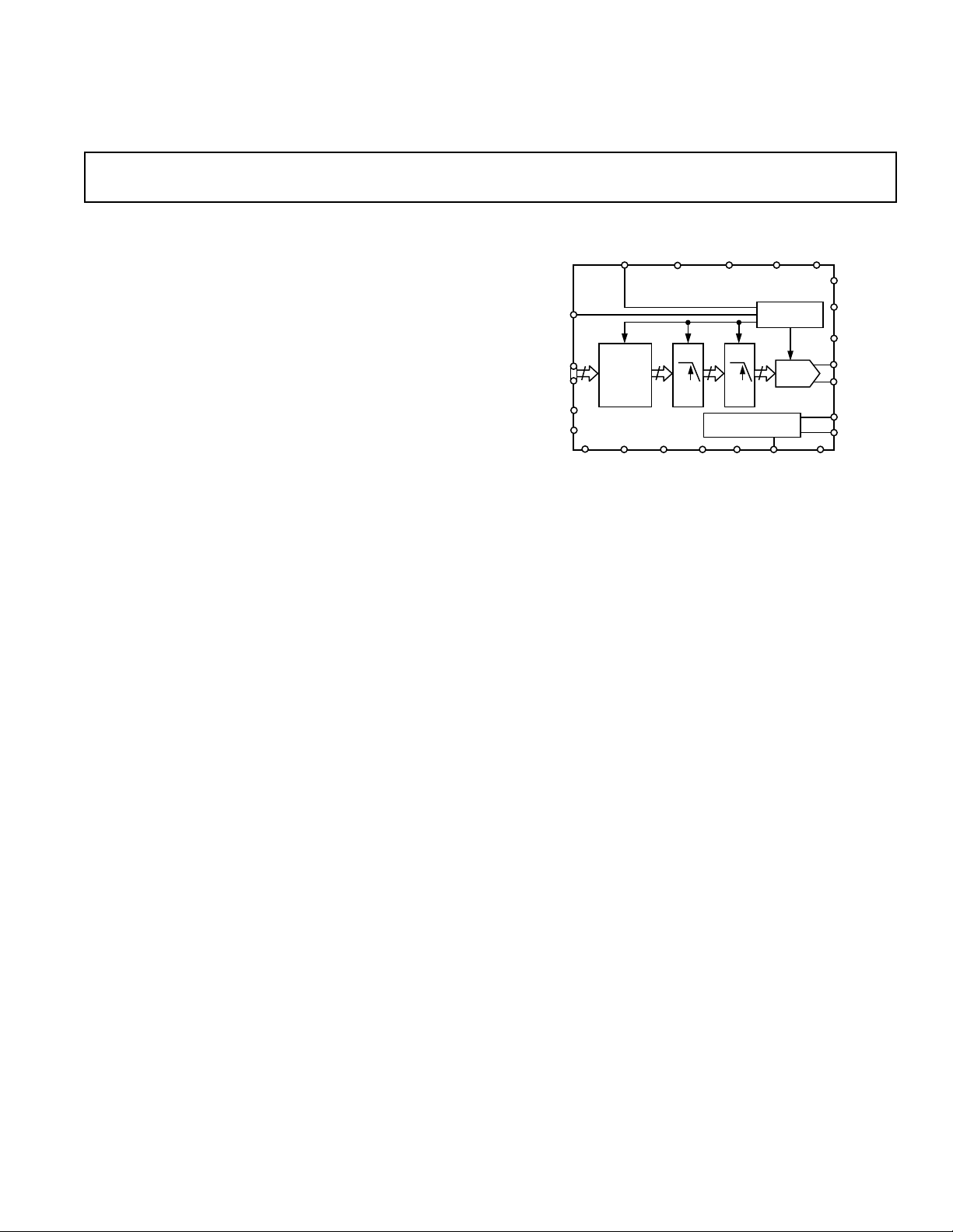
FUNCTIONAL BLOCK DIAGRAM
Edge-triggered input latches, a 4× clock multiplier, and a tem-
perature compensated bandgap reference have also been integrated to provide a complete monolithic DAC solution. Flexible
supply options support +3 V and +5 V CMOS logic families.
TTL logic levels can also be accommodated by reducing the
AD9774 digital supply.
The on-chip reference and control amplifier are configured for
maximum accuracy and flexibility. The AD9774 can be driven
by the on-chip reference or by a variety of external reference
voltages. The full-scale current of the AD9774 can be adjusted
over a 2 mA to 20 mA range, thus providing additional gain
ranging capabilities.
The AD9774 is available in a 44-lead MQFP package. It is
specified for operation over the industrial temperature range.
PRODUCT HIGHLIGHTS
1. On-Chip 4× interpolation filter eases analog reconstruction
filter requirements by suppressing the first three images by 69 dB.
2. Low glitch and fast settling time provide outstanding dynamic
performance for waveform reconstruction or digital synthesis
requirements, including communications.
3. On-chip, edge-triggered input CMOS latches interface readily
to CMOS and TTL logic families. The AD9774 can support
input data rates up to 32 MSPS.
4. A temperature compensated, 1.20 V bandgap reference is
included on-chip, providing a complete DAC solution. An
external reference may also be used.
5. The current output(s) of the AD9774 can easily be configured
for various single-ended or differential circuit topologies.
6. On-chip clock multiplier generates all the high-speed clocks
required by the internal interpolation filters. Both 2× and 4×
clocks are generated from the lower rate data clock supplied
by the user.
One Technology Way, P.O. Box 9106, Norwood, MA 02062-9106, U.S.A.
Tel: 781/329-4700 World Wide Web Site: http://www.analog.com
Fax: 781/326-8703 © Analog Devices, Inc., 1998

AD9774–SPECIFICATIONS
DC SPECIFICATIONS
(T
to T
MIN
, AVDD = +5 V, PLLVDD = +5 V, DVDD = +5 V, I
MAX
= 20 mA, unless otherwise noted)
OUTFS
Parameter Min Typ Max Units
RESOLUTION 14 Bits
DC ACCURACY
1
Integral Linearity Error (INL)
T
= +25°C ±4 LSB
A
to T
T
MIN
MAX
Differential Nonlinearity (DNL)
= +25°C ±3 LSB
T
A
T
to T
MIN
MAX
Monotonicity (12-Bit) GUARANTEED OVER RATED SPECIFICATION TEMPERATURE RANGE
ANALOG OUTPUT
Offset Error –0.025 +0.025 % of FSR
Gain Error (Without Internal Reference) –7 ±1 +7 % of FSR
Gain Error (With Internal Reference) +7.5 ±1 +7.5 % of FSR
Full-Scale Output Current
2
20 mA
Output Compliance Range 1.25 V
Output Resistance 100 kΩ
Output Capacitance 5 pF
REFERENCE OUTPUT
Reference Voltage 1.14 1.20 1.26 V
Reference Output Current
3
1 µA
REFERENCE INPUT
Input Compliance Range 0.1 1.25 V
Reference Input Resistance 1 MΩ
TEMPERATURE COEFFICIENTS
Unipolar Offset Drift 0 ppm of FSR/°C
Gain Drift (Without Internal Reference) ±50 ppm of FSR/°C
Gain Drift (With Internal Reference) ±100 ppm of FSR/°C
Reference Voltage Drift ±100 ppm of FSR/°C
POWER SUPPLY
AVDD
Voltage Range
Analog Supply Current (I
Analog Supply Current in SLEEP Mode (I
4
) 26.5 32 mA
AVDD
) 3.2 5 mA
AVDD
2.7 5.0 5.5 V
PLLVDD
Voltage Range 2.7 5.0 5.5 V
Clock Multiplier Supply Current (I
)1317mA
PLLVDD
DVDD
Voltage Range 2.7 5.0 5.5 V
Digital Supply Current at 5 V (I
Digital Supply Current at 5 V in SNOOZE Mode (I
Digital Supply Current at 3 V (I
Nominal Power Dissipation
AVDD and DVDD at 3 V
AVDD and DVDD at 5 V
6
6
Power Supply Rejection Ratio (PSRR)
Power Supply Rejection Ratio (PSRR)
5
DVDD
DVDD
)
) 42.0 50.0 mA
5
)
DVDD
123.0 140.0 mA
62.0 mA
415 mW
7
– AVDD –0.2 +0.2 % of FSR/V
7
– PLLVDD –0.025 +0.025 % of FSR/V
1125 mW
Power Supply Rejection Ratio (PSRR)7 – DVDD –0.025 +0.025 % of FSR/V
OPERATING RANGE –40 +85 °C
NOTES
1
Measured at IOUTA driving a virtual ground.
2
Nominal full-scale current, IOUTFS, is 32 × the I
3
Use an external amplifier to drive any external load.
4
For operation below 3 V, it is recommended that the output current be reduced to 12 mA or less to maintain optimum performance.
5
Measured at f
6
Measured as unbuffered voltage output into 50 Ω R
7
±5% power supply variation.
Specifications subject to change without notice.
= 25 MSPS and f
CLOCK
= 1.01 MHz.
OUT
current.
REF
at IOUTA and IOUTB, f
LOAD
= 32 MSPS and f
CLOCK
= 12.8 MHz.
OUT
–2–
REV. B
AD9774
(T
to T
, AVDD = +5 V, PLLVDD = +5 V, DVDD = +5 V, I
MAX
DYNAMIC SPECIFICATIONS
MIN
Coupled Output, 50 ⍀ Doubly Terminated, unless otherwise noted)
Parameter Min Typ Max Units
DYNAMIC PERFORMANCE
Maximum Output Update Rate w/DVDD = 5 V 128 MSPS
Maximum Output Update Rate w/DVDD = 3 V 100 128 MSPS
Output Settling Time (t
Output Propagation Delay (t
Glitch Impulse 5 pV-s
Output Rise Time (10% to 90%)
Output Fall Time (10% to 90%)
Output Noise (I
OUTFS
) (to 0.025%) 35 ns
ST
) 55 Clocks
PD
1
1
2.5 ns
2.5 ns
= 20 mA) 50 pA/√Hz
AC LINEARITY TO NYQUIST
Spurious-Free Dynamic Range (SFDR) to Nyquist
= 25 MSPS; f
f
CLOCK
= 1.01 MHz
OUT
0 dBFS Output 79 dB
–6 dBFS Output 86 dB
–12 dBFS Output 75 dB
–18 dBFS Output 75 dB
= 32 MSPS; f
f
CLOCK
= 32 MSPS; f
f
CLOCK
f
= 32 MSPS; f
CLOCK
f
= 32 MSPS; f
CLOCK
= 1.01 MHz 78 dB
OUT
= 5.01 MHz 77 dB
OUT
= 10.01 MHz 79 dB
OUT
= 13.01 MHz 78 dB
OUT
Total Harmonic Distortion (THD)
= 25 MSPS; f
f
CLOCK
= 1.01 MHz; 0 dBFS –75 dB
OUT
Signal-to-Noise Ratio (SNR)
f
= 25 MSPS; f
CLOCK
NOTES
1
Propagation delay is delay from data input to DAC update.
2
Measured single-ended into 50 Ω load.
Specifications subject to change without notice.
= 1.01 MHz; 0 dBFS 76 dB
OUT
= 20 mA, Differential Transformer
OUTFS
1
2
DIGITAL SPECIFICATIONS
MIN
, AVDD = +5 V, PLLVDD = +5 V, DVDD = +5 V, I
MAX
= 20 mA unless otherwise noted)
OUTFS
(T
to T
Parameter Min Typ Max Units
DIGITAL INPUTS
Logic “1” Voltage @ DVDD = +5 V 3.5 5 V
Logic “1” Voltage @ DVDD = +3 V 2.1 3 V
Logic “0” Voltage @ DVDD = +5 V 0 1.3 V
Logic “0” Voltage @ DVDD = +3 V 0 0.9 V
Logic “1” Current –10 +10 µA
Logic “0” Current –10 +10 µA
Input Capacitance 5 pF
Input Setup Time (t
Input Hold Time (t
Latch Pulsewidth (t
) 2.5 ns
S
) 1.5 ns
H
)4ns
LPW
DB0–DB11
CLOCK
IOUTA
OR
IOUTB
t
S
t
PD
t
t
0.025%
LPW
ST
t
H
0.025%
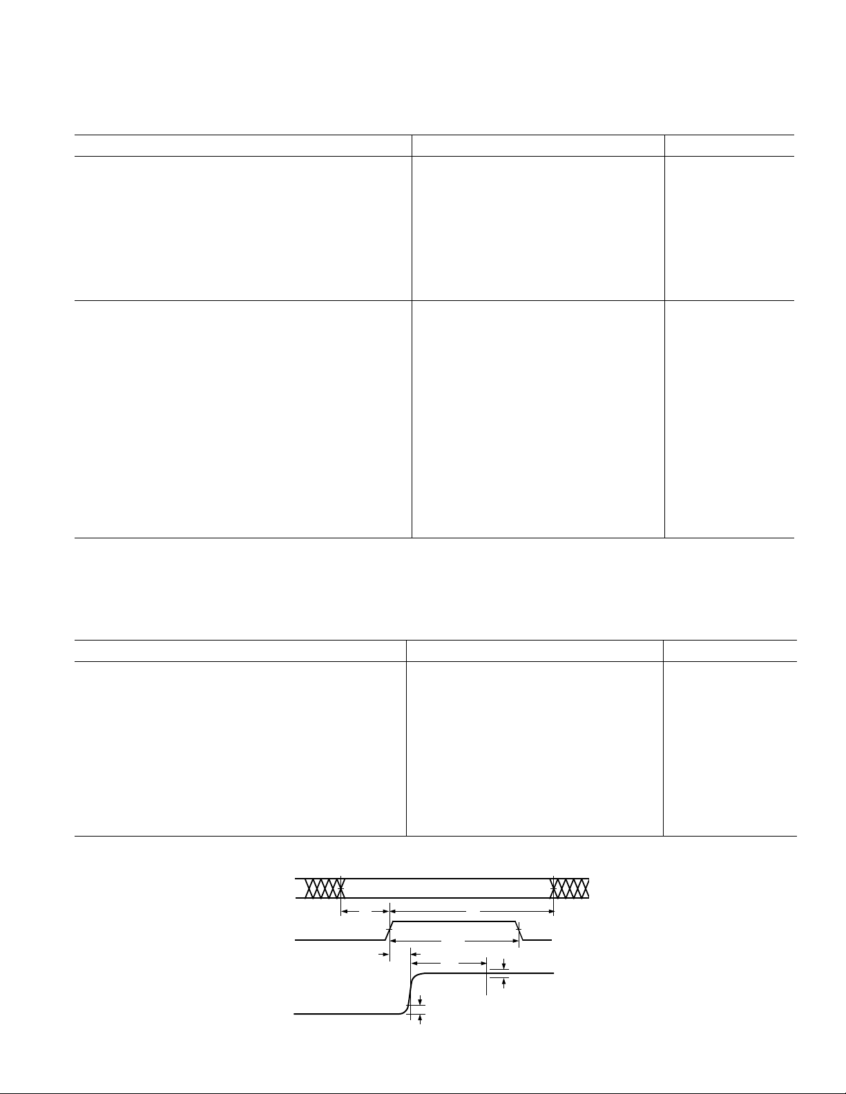
Figure 1. Timing Diagram
–3–REV. B
AD9774–SPECIFICATIONS
(T
to T
, AVDD = +2.7 V to +5.5 V, DVDD = +2.7 V to +5.5 V, I
MAX
DIGITAL FILTER SPECIFICATIONS
MIN
otherwise noted)
Parameter Min Typ Max Units
MAXIMUM INPUT CLOCK RATE (f
CLOCK
)
DVDD = 5 V 32 MSPS
DVDD = 3 V 25 32 MSPS
= 20 mA unless
OUTFS
DIGITAL FILTER CHARACTERISTICS
Passband Width
Passband Width: 0.01 dB 0.414 f
Passband Width: 0.1 dB 0.420 f
Passband Width: –3 dB 0.482 f
1
: 0.005 dB 0.410 f
OUT/fCLOCK
OUT/fCLOCK
OUT/fCLOCK
OUT/fCLOCK
LINEAR PHASE (FIR IMPLEMENTATION)
STOPBAND REJECTION
CLOCK
CLOCK
to 3.419 f
to 1.409 f
0.591 f
0.591 f
GROUP DELAY
CLOCK
CLOCK
2
–69.5 dB
–79.5 dB
38 Input Clocks
IMPULSE RESPONSE DURATION
–40 dB 53 Input Clocks
–60 dB 62 Input Clocks
NOTES
1
Excludes sinx/x characteristic of DAC.
2
Defined as the number of data clock cycles between impulse input and peak of output response.
Specifications subject to change without notice.
ABSOLUTE MAXIMUM RATINGS*
With
Respect
Parameter to Min Max Units
AVDD ACOM –0.3 +6.5 V
DVDD DCOM –0.3 +6.5 V
PLLVDD PLLCOM –0.3 +6.5 V
ACOM DCOM –0.3 +0.3 V
PLLCOM ACOM –0.3 +0.3 V
PLLCOM DCOM –0.3 +0.3 V
AVDD DVDD –6.5 +6.5 V
PLLVDD DVDD –0.3 +6.5 V
PLLVDD AVDD –0.3 +6.5 V
Model Range Description Option*
AD9774AS –40°C to +85°C 44-Lead MQFP S-44
AD9774EB Evaluation Board
*S = Metric Quad Flatpack.
THERMAL CHARACTERISTIC
Thermal Resistance
44-Lead MQFP
= 53.2°C/W
θ
JA
θ
= 19°C/W
JC
ORDERING GUIDE
Temperature Package Package
CLKIN, CLK4×IN DVDD –0.3 +6.5 V
SLEEP, SNOOZE DCOM –0.3 DVDD + 0.3 V
Digital Inputs DCOM –0.3 DVDD + 0.3 V
PLL DIVIDE, LPF ACOM –0.3 PLLVDD + 0.3 V
PLLLOCK ACOM –0.3 PLLVDD + 0.3 V
VCO IN/EXT ACOM –0.3 PLLVDD + 0.3 V
IOUTA/IOUTB ACOM –0.3 AVDD + 0.3 V
REFIO, FSADJ ACOM –0.3 AVDD + 0.3 V
FSADJ ACOM –0.3 AVDD + 0.3 V
ICOMP ACOM –0.3 AVDD + 0.3 V
REFCOM ACOM –0.3 +0.3 V
Junction Temperature +150 °C
Storage Temperature –65 +150 °C
Lead Temperature +300 °C
(10 sec)
*Stresses above those listed under Absolute Maximum Ratings may cause perma-
nent damage to the device. This is a stress rating only; functional operation of the
device at these or any other conditions above those indicated in the operational
sections of this specification is not implied. Exposure to absolute maximum ratings
for extended periods may effect device reliability.
–4–
REV. B
AD9774
WARNING!
ESD SENSITIVE DEVICE
0
–20
–40
–60
–80
–100
–120
OUTPUT – dBFS
–140
–160
–180
0 0.5
FREQUENCY – DC TO 23 f
1.0
1.5
CLOCK
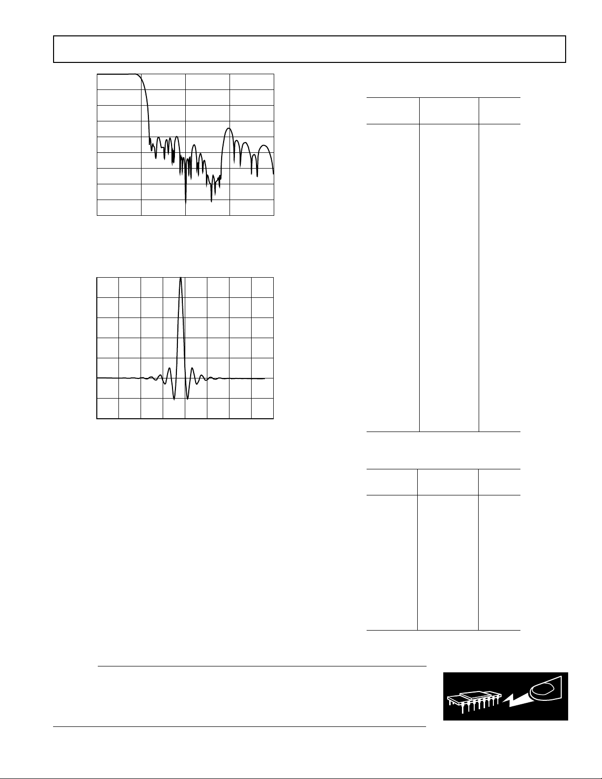
Figure 2a. FIR Filter Frequency Response
1.0
0.8
0.6
0.4
0.2
NORMALIZED OUTPUT
0.0
–0.2
–0.4
0
10
20 30 40
TIME – Samples
60 70
50
Figure 2b. FIR Filter Impulse Response
2.0
80
Table I. Integer Filter Coefficients for First Stage Interpolation Filter (55-Tap Halfband FIR Filter)
Lower Upper Integer
Coefficient Coefficient Value
H(1) H(55) –1
H(2) H(54) 0
H(3) H(53) 3
H(4) H(52) 0
H(5) H(51) –7
H(6) H(50) 0
H(7) H(49) 15
H(8) H(48) 0
H(9) H(47) –28
H(10) H(46) 0
H(11) H(45) 49
H(12) H(44) 0
H(13) H(43) –81
H(14) H(42) 0
H(15) H(41) 128
H(16) H(40) 0
H(17) H(39) –196
H(18) H(38) 0
H(19) H(37) 295
H(20) H(36) 0
H(21) H(35) –447
H(22) H(34) 0
H(23) H(33) 706
H(24) H(32) 0
H(25) H(31) –1274
H(26) H(30) 0
H(27) H(29) 3976
H(28) 6276
Table II. Integer Filter Coefficients for Second Stage Interpolation Filter (23-Tap Halfband FIR Filter)
Lower Upper Integer
Coefficient Coefficient Value
H(1) H(23) –6
H(2) H(22) 0
H(3) H(21) 37
H(4) H(20) 0
H(5) H(19) –125
H(6) H(18) 0
H(7) H(17) 316
H(8) H(16) 0
H(9) H(15) –736
H(10) H(14) 0
H(11) H(13) 2562
H(12) 4096
CAUTION
ESD (electrostatic discharge) sensitive device. Electrostatic charges as high as 4000 V readily
accumulate on the human body and test equipment and can discharge without detection.
Although the AD9774 features proprietary ESD protection circuitry, permanent damage may
occur on devices subjected to high energy electrostatic discharges. Therefore, proper ESD
precautions are recommended to avoid performance degradation or loss of functionality.
–5–REV. B
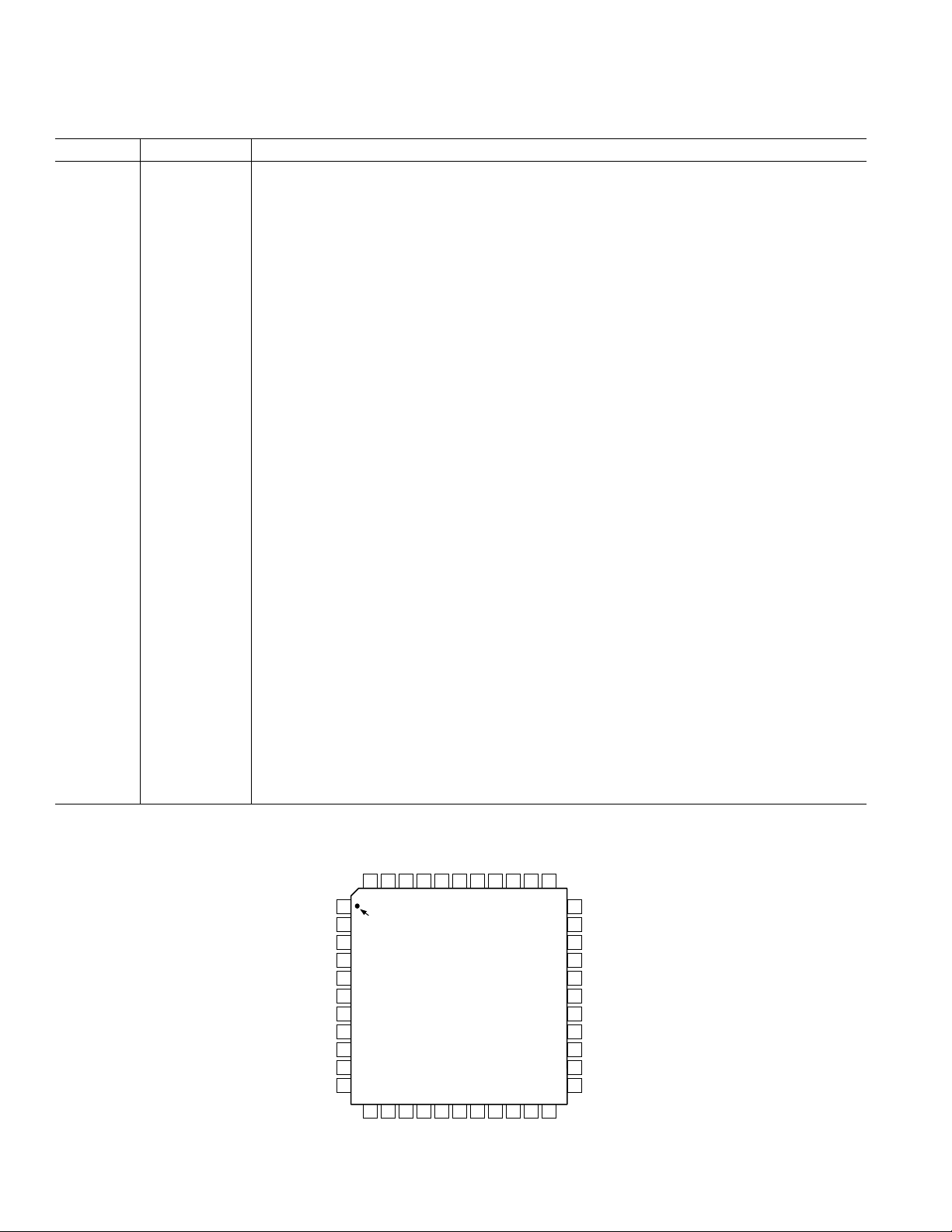
AD9774
PIN FUNCTION DESCRIPTIONS
Pin No. Name Description
1, 19, 40, 44 DCOM Digital Common.
2 DB13 Most Significant Data Bit (MSB).
3–14 DB12–DB1 Data Bits 1–12.
15 DB0 Least Significant Data Bit (LSB).
16, 17, 42 NC No Internal Connection.
18, 41 DVDD Digital Supply Voltage (+2.7 V to +5.5 V).
20 CLK IN/OUT Clock Input when PLL Clock Multiplier enabled. Clock Output when PLL Clock Multiplier
disabled. Data latched on rising edge.
21 PLLLOCK Phase Lock Loop Lock Signal. Active High indicates PLL is locked to input clock.
22 CLK4×IN External 4× Clock Input when PLL is disabled. No Connect when internal PLL is active.
23 PLLDIVIDE PLL Range Control Pin. Connect to PLLCOM if CLKIN is above 10 MSPS. Connect to
PLLVDD if CLKIN is between 10 MSPS and 5.5 MSPS.
24 VCO IN/EXT Internal Voltage Controlled Oscillator (VCO) Enable/Disable Pin. Connect to PLLVDD to enable
VCO. Connect to PLLCOM to disable VCO and drive CLK4×IN with external VCO output.
25 LPF PLL Loop Filter Node. Connect to external VCO control input if internal VCO disabled.
26 PLLVDD Phase Lock Loop (PLL) Supply Voltage (+2.7 V to +5.5 V). Must be set to similar voltage as DVDD.
27 PLLCOM Phase Lock Loop Common.
28 PLLENABLE Phase Lock Loop Enable. Connect to PLLVDD to enable. Connect to PLLCOM to disable.
29 UNUSED Factory Test. Leave Open.
30 REFLO Reference Ground when Internal 1.2 V Reference Used. Connect to AVDD to disable internal
reference.
31 REFIO Reference Input/Output. Serves as reference input when internal reference disabled (i.e., tie REFLO
to AVDD). Serves as 1.2 V reference output when internal reference activated (i.e., tie REFLO to
ACOM). Requires 0.1 µF capacitor to ACOM when internal reference activated.
32 FSADJ Full-Scale Current Output Adjust.
33 REFCOMP Noise Reduction Node. Add 0.1 µF to AVDD.
34 ACOM Analog Common.
35 AVDD Analog Supply Voltage (+2.7 V to +5.5 V).
36 IOUTB Complementary DAC Current Output. Full-scale current when all data bits are 0s.
37 IOUTA DAC Current Output. Full-scale current when all data bits are 1s.
38 ICOMP Internal bias node for switch driver circuitry. Decouple to ACOM with 0.1 µF capacitor.
39 SLEEP Power-Down Control Input. Active High. Connect to DCOM if not used.
43 SNOOZE SNOOZE Control Input. Deactivates 4× interpolation filter to reduce digital power consumption
only. Active High. Connect to DCOM if not used.
PIN CONFIGURATION
DCOM
1
DCOM
DB13
DB12
DB11
DB10
DB9
DB8
DB7
DB6
DB5
DB4
NC = NO CONNECT
PIN 1
IDENTIFIER
2
3
4
5
6
7
8
9
10
11
12 13 14 15 16 17 18 19 20 21 22
DB3
SNOOZE
NC
DB2
DB1
DVDD
SLEEP
DCOM
40 39 3841424344 36 35 3437
AD9774
TOP VIEW
(Not to Scale)
NC
NC
DB0
–6–
ICOMP
DVDD
IOUTB
IOUTA
DCOM
CLK IN/OUT
ACOM
AVDD
CLK43IN
PLLLOCK
33
REFCOMP
32
FSADJ
31
REFIO
30
REFLO
29
UNUSED
28
PLLENABLE
27
PLLCOM
26
PLLVDD
25
LPF
24
VCO IN/EXT
23
PLLDIVIDE
REV. B
AD9774
DEFINITIONS OF SPECIFICATIONS
Linearity Error (Also Called Integral Nonlinearity or INL)
Linearity error is defined as the maximum deviation of the actual
analog output from the ideal output, determined by a straight
line drawn from zero to full scale.
Differential Nonlinearity (or DNL)
DNL is the measure of the variation in analog value, normalized
to full scale, associated with a 1 LSB change in digital input code.
Monotonicity
A D/A converter is monotonic if the output either increases or
remains constant as the digital input increases.
Offset Error
The deviation of the output current from the ideal of zero is
called offset error. For IOUTA, 0 mA output is expected when
the inputs are all 0s. For IOUTB, 0 mA output is expected
when all inputs are set to 1s.
Gain Error
The difference between the actual and ideal output span. The
actual span is determined by the output when all inputs are set
to 1s, minus the output when all inputs are set to 0s.
Output Compliance Range
The range of allowable voltage at the output of a current-output
DAC. Operation beyond the maximum compliance limits may
cause either output stage saturation or breakdown, resulting in
nonlinear performance.
Temperature Drift
Temperature drift is specified as the maximum change from the
ambient (+25°C) value to the value at either T
MIN
or T
MAX
. For
offset and gain drift, the drift is reported in ppm of full-scale
range (FSR) per degree C. For reference drift, the drift is reported in ppm per degree C.
Power Supply Rejection
The maximum change in the full-scale output as the supplies
are varied from nominal to minimum and maximum specified
voltages.
Settling Time
The time required for the output to reach and remain within a
specified error band about its final value, measured from the
start of the output transition.
Glitch Impulse
Asymmetrical switching times in a DAC give rise to undesired
output transients that are quantified by a glitch impulse. It is
specified the net area of the glitch in pV-s.
Spurious-Free Dynamic Range
The difference, in dB, between the rms amplitude of the output
signal and the peak spurious signal over the specified bandwidth.
Total Harmonic Distortion
THD is the ratio of the rms sum of the first six harmonic components to the rms value of the measured input signal. It is
expressed as a percentage or in decibels (dB).
Signal-to-Noise Ratio (SNR)
S/N is the ratio of the rms value of the measured output signal
to the rms sum of all other spectral components below the
Nyquist frequency, excluding the first six harmonics and dc.
The value for SNR is expressed in decibels.
Passband
Frequency band in which any input applied therein passes
unattenuated to the DAC output.
Stopband Rejection
The amount of attenuation of a frequency outside the passband
applied to the DAC, relative to a full-scale signal applied at the
DAC input within the passband.
Group Delay
Number of input clocks between an impulse applied at the
device input and peak DAC output current.
Impulse Response
Response of the device to an impulse applied to the input.
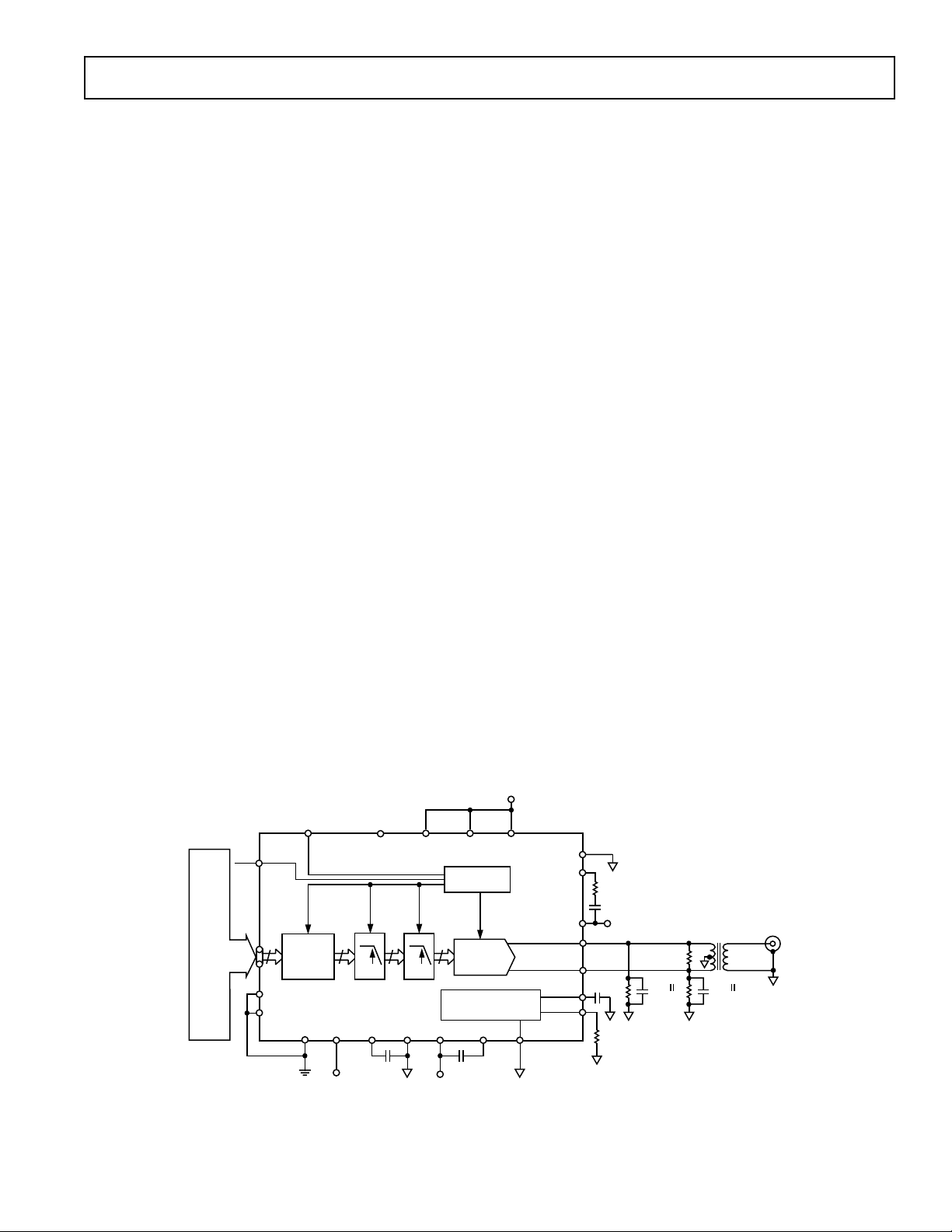
CLK
IN/OUT
TEKTRONIX AWG-2021
OPTION 4
DIGITAL
DATA
14
SNOOZE
SLEEP
CLK43IN
13 23 43
EDGE
TRIGGERED
LATCHES
DCOM
PLLLOCK
14 14 14
23 23
AD9774
ICOMP
DVDD
+3V
D
Figure 3. Basic AC Characterization Test Setup
0.1mF
ENABLE
ACOM
PLL
VCO
IN/EXT
PLL CLOCK
MULTIPLIER
14-BIT DAC
+1.2V REFERENCE
AND CONTROL AMP
REFCOMP
AVDD
0.1mF
+5V
A
+3V
D
43
PLL
DIVIDE
PLLCOM
PLLVDD
REFLO
LPF
IOUTA
IOUTB
REFIO
FSADJ
0.1mF
1.5kV
0.01mF
+3V
1.91kV
D
100V
50V
20pF
TO HP3589A
SPECTRUM/NETWORK
ANALYZER
50V INPUT
MINI-CIRCUITS
T1-1T
50V
20pF
–7–REV. B
AD9774
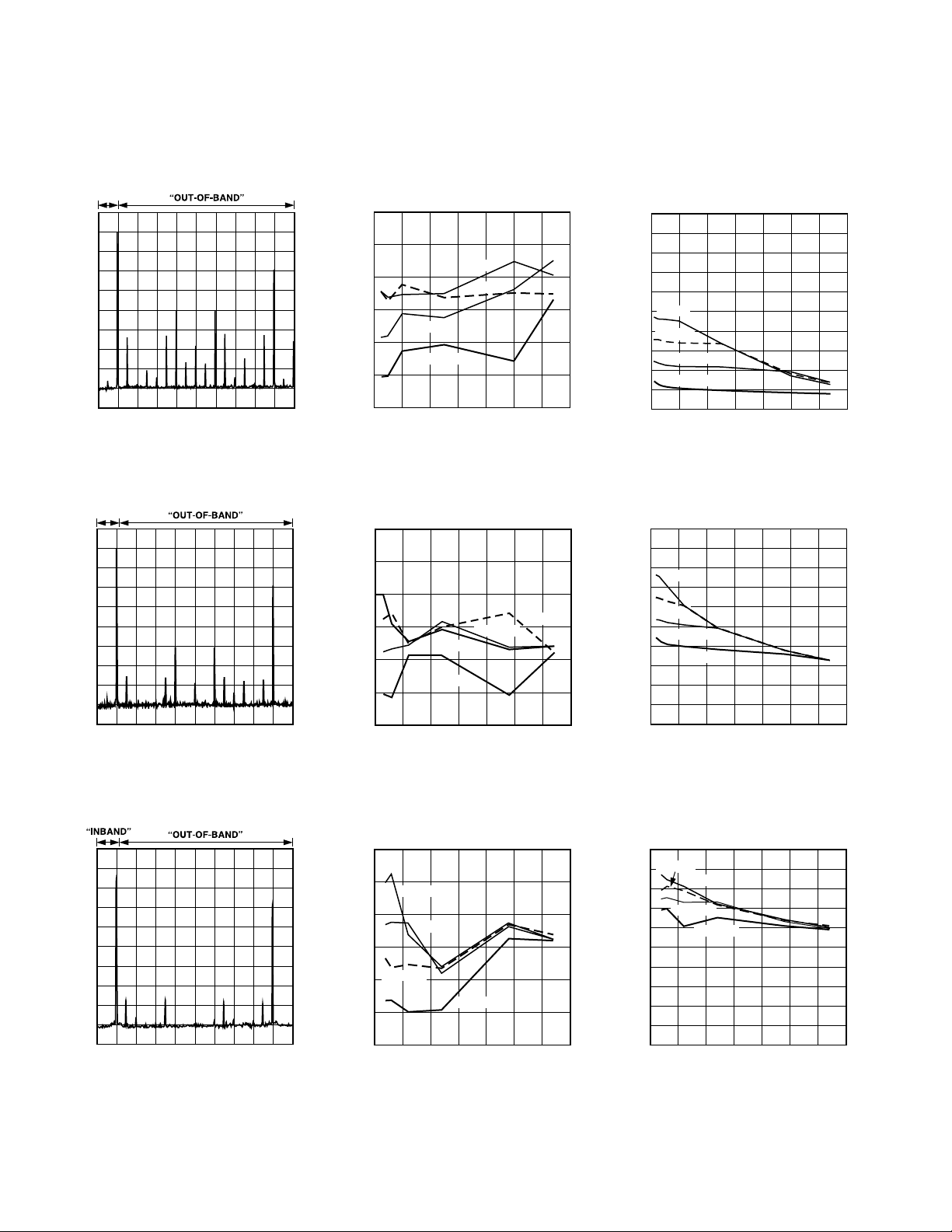
Typical AC Characterization Curves
(AVDD = +5 V, PLLVDD = +3 V, DVDD = +3 V, I
noted. Note: PLLVDD = +5 V and DVDD = +5 V for Figures 4, 5 and 6.)
“INBAND”
10
0
–10
–20
–30
–40
–50
10dB – DIV
–60
–70
–80
–90
0 128.0
25.6 51.2 76.8 102.4
Figure 4. Single Tone Spectral Plot
@ 32 MSPS w/f
×
CLKIN)
4
“INBAND”
10
0
–10
–20
–30
–40
–50
10dB – DIV
–60
–70
–80
–90
0 64.012.8 25.6 38.4 51.2
Figure 7. Single Tone Spectral Plot
@ 16 MSPS w/f
4
×
CLKIN)
MHz
= 12.8 MHz (DC to
OUT
MHz
= 6.4 MHz (DC to
OUT
= 20 mA, 50 ⍀ Doubly Terminated Load, Differential Output, TA = +25ⴗC, unless otherwise
OUTFS
90
85
80
75
SFDR – dBc
70
65
60
–12dBFS
–18dBFS
02 14
4681012
Figure 5. “Inband” SFDR vs. f
@ 32 MSPS (DC to CLKIN/2)
90
85
80
75
SFDR – dBc
70
65
60
0
–18dBFS
17
23456
Figure 8. “Inband” SFDR vs. f
@ 16 MSPS (DC to CLKIN/2)
f
OUT
0dBFS
f
OUT
0dBFS
–6dBFS
– MHz
–12dBFS
– MHz
–6dBFS
OUT
OUT
85
80
75
70
65
0dBFS
60
55
–6dBFS
SFDR – dBc
50
Figure 6. “Out-of-Band” SFDR vs. f
–12dBFS
45
–18dBFS
40
35
0
214
4 6 8 10 12
f
– MHz
OUT
OUT
@ 32 MSPS (CLKIN/2 to 3 1/2 CLKIN)
85
80
75
0dBFS
70
65
–6dBFS
60
–12dBFS
55
SFDR – dBc
50
45
40
35
–18dBFS
0
23456
17
f
– MHz
OUT
Figure 9. “Out-of-Band” SFDR vs.
@ 16 MSPS (CLKIN/2 to 3 1/2
f
OUT
CLKIN)
10
0
–10
–20
–30
–40
–50
10dB – DIV
–60
–70
–80
–90
0
6.4 12.8 19.2 25.6
MHz
32.0
Figure 10. Single Tone Spectral Plot
f
@ 8 MSPS w/f
OUT
×
CLKIN)
to 4
= 3.2 MHz (DC
OUT
90
85
0dBFS
80
75
SFDR – dBc
70
65
60
–6dBFS
–12dBFS
–18dBFS
0
1 1.5 2 2.5 3
0.5 3.5
f
OUT
– MHz
Figure 11. “Inband” SFDR vs. f
@ 8 MSPS (DC to CLKIN/2)
–8–
OUT
85
–6dBFS
80
75
70
65
60
55
SFDR – dBc
50
45
40
35
0dBFS
–12dBFS
–18dBFS
0
0.5 3.5
1 1.5 2 2.5 3
f
– MHz
OUT
Figure 12. “Out-of-Band” SFDR vs.
f
@ 8 MSPS (CLKIN/2 to 3 1/2
OUT
CLKIN)
REV. B
 Loading...