®
14-BIT DAC
2 FIR
INTER-
POLATION
FILTE
R
EDGE-
TRIGGERED
LATCHES
CLOCK DISTRIBUTION
AND MODE SELECT
2/4
MUX
CONTROL
FILTER
CONTROL
1/2
1
PLL CLOCK
MULTIPLIER
+1.2V REFERENCE
AND CONTROL AMP
AD9772A
CLKCOM
CLKVDD MOD0 MOD1 RESET
PLLLOCK
DIV0
DIV1
CLK+
CLK–
DATA
INPUTS
(DB13...
DB0)
SLEEP
DCOM DVDD ACOM AVDD
REFLO
PLLCOM
LPF
PLLVDD
I
OUTA
I
OUTB
REFIO
FSADJ
ZEROSTUFF
MUX
14-Bit, 160 MSPS TxDAC+
with 2 Interpolation Filter
AD9772A
FEATURES
Single 3.1 V to 3.5 V Supply
14-Bit DAC Resolution and Input Data Width
160 MSPS Input Data Rate
67.5 MHz Reconstruction Pass Band @ 160 MSPS
74 dBc SFDR @ 25 MHz
2 Interpolation Filter with High- or Low-Pass Response
73 dB Image Rejection with 0.005 dB Pass-band Ripple
Zero -Stufng Option for Enhanced Direct IF Performance
Internal 2/4 Clock Multiplier
250 mW Power Dissipation; 13 mW with Power-Down
Mode
48-Lead LQFP Package
APPLICATIONS
Communication Transmit Channel
W-CDMA Base Stations, Multicarrier Base Stations,
Direct IF Synthesis, Wideband Cable Systems
Instrumentation
GENERAL DESCRIPTION
The AD9772A is a single-supply, oversampling, 14-bit digital-to-analog converter (DAC) optimized for baseband or IF
waveform reconstruction applications requiring exceptional
dynamic range. Manufactured on an advanced CMOS process, it integrates a complete, low distortion 14-bit DAC with
a 2 digital interpolation lter and clock multiplier. The onchip PLL clock multiplier provides all the necessary clocks
for the digital lter and the 14-bit DAC. A exible differential
clock input allows for a single-ended or differential clock
driver for optimum jitter performance.
For baseband applications, the 2 digital interpolation lter
provides a low-pass response, thus providing as much as a
threefold reduction in the complexity of the analog reconstruction lter. It does so by multiplying the input data rate by a
factor of 2 while suppressing the original upper in-band image
by more than 73 dB. For direct IF applications, the 2 digital
interpolation lter response can be recongured to select the
upper in-band image (i.e., high-pass response) while suppressing the original baseband image. To increase the signal
the higher IF images and their pass-band atness in di
applications, the AD9772A also features a zero-stufng option in which the data following the 2 interpolation lter is
upsampled by a factor of 2 by inserting midscale data samples.
The AD9772A can reconstruct full-scale waveforms with bandwidths as high as 67.5 MHz while operating at an input data
rate of 160 MSPS. The 14-bit DAC provides differential cur
outputs to support differential or single-ended applications.
REV. B
Information furnished by Analog Devices is believed to be accurate and
reliable. However, no responsibility is assumed by Analog Devices for its
use, nor for any infringements of patents or other rights of third parties
that may result from its use. No license is granted by implication or otherwise under any patent or patent rights of Analog Devices. Trademarks
and registered trademarks are the property of their respective companies.
level of
rect IF
rent
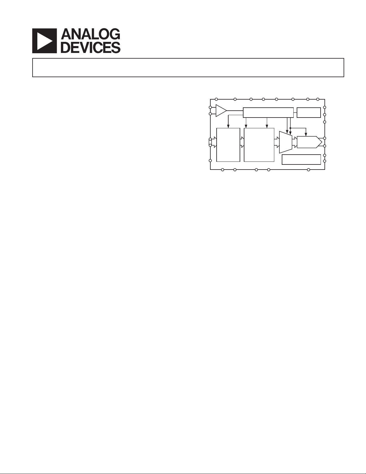
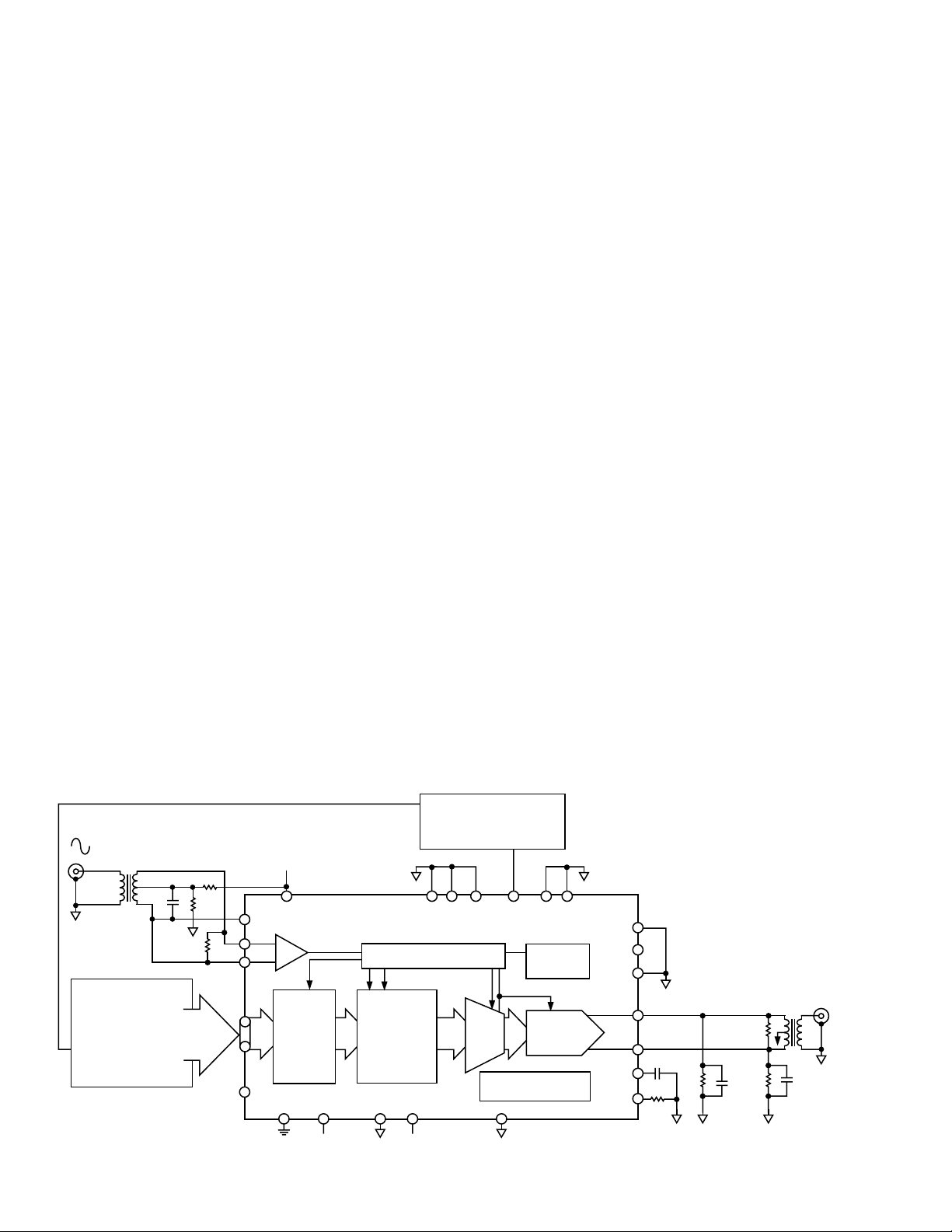
FUNCTIONAL BLOCK DIAGRAM
A
segmented current source architecture is combined with a
proprietary switching technique to reduce spurious components
and enhance dynamic performance. Matching between the two
current outputs ensures enhanced dynamic performance in a
differential output conguration. The differential current outputs
may be fed into a transformer or a differential op amp topology
to obtain a single-ended output voltage using an appropriate
resistive load.
The on-chip band gap reference and control amplier are congured for maximum accuracy and exibility. The AD9772A
can be driven by the on-chip reference or by a variety of external
reference voltages. The full-scale current of the AD9772A can be
adjusted over a 2 mA to 20 mA range, thus providing additional
gain ranging capabilities.
The AD9772A is available in a 48-lead LQFP package and is
specied for operation over the industrial temperature range of
–40°C to +85°C.
PRODUCT HIGHLIGHTS
1. A exible, low power 2 interpolation lter supporting recon-
struction bandwidths of up to 67.5 MHz can be congured
for a low- or high-pass response with 73 dB of image rejection
for traditional baseband or direct IF applications.
2. A zero-stufng option enhances direct IF applications.
3. A low glitch, fast settling 14-bit DAC provides exceptional
dynamic range for both baseband and direct IF waveform
reconstruction applications.
4. The AD9772A digital interface, consisting of edge-triggered
latches and a exible differential or single-ended clock input,
can support input data rates up to 160 MSPS.
5. On-chip PLL clock multiplier generates all of the internal high
speed clocks required by the interpolation lter and DAC.
6. The current output(s) of the AD9772A can easily be congured
for various single-ended or differential circuit topologies.
One Technology Way, P.O. Box 9106, Norwood, MA 02062-9106, U.S.A.
Tel: 781/329-4700 www.analog.com
Fax: 781/326-8703 © 2003 Analog Devices, Inc. All rights reserved.

AD9772A–SPECIFICATIONS
DC SPECIFICATIONS
(T
to T
MIN
, AVDD = 3.3 V, CLKVDD = 3.3 V, PLLVDD = 0 V, DVDD = 3.3 V, I
MAX
= 20 mA, unless otherwise noted.)
OUTFS
Parameter Min Typ Max Unit
RESOLUTION 14 Bits
DC ACCURACY
1
Integral Linearity Error (INL) ±3.5 LSB
Differential Nonlinearity (DNL) ±2.0 LSB
Monotonicity (12-Bit) Guaranteed over Specied Temperature Range
ANALOG OUTPUT
Offset Error –0.025 +0.025 % of FSR
Gain Error (without Internal Reference) –2 ±0.5 +2 % of FSR
Gain Error (with Internal Reference) –5 ±1.5 +5 % of FSR
Full-Scale Output Current2 20 mA
Output Compliance Range –1.0 +1.25 V
Output Resistance 200 kW
Output Capacitance 3 pF
REFERENCE OUTPUT
Reference Voltage 1.14 1.20 1.26 V
Reference Output Current
3
1 µA
REFERENCE INPUT
Input Compliance Range 0.1 1.25 V
Reference Input Resistance (REFLO = 3 V) 10 MW
Small Signal Bandwidth 0.5 MHz
TEMPERATURE COEFFICIENTS
Unipolar Offset Drift 0 ppm of FSR/°C
Gain Drift (without Internal Reference) ±50 ppm of FSR/°C
Gain Drift (with Internal Reference) ±100 ppm of FSR/°C
Reference Voltage Drift ±50 ppm/°C
POWER SUPPLY
AVDD
Voltage Range 3.1 3.3 3.5 V
Analog Supply Current (I
Analog Supply Current in SLEEP Mode (I
) 34 37 mA
AVDD
) 4.3 6 mA
AVDD
DVDD1, DVDD2
Voltage Range 3.1 3.3 3.5 V
Digital Supply Current (I
DVDD1
+ I
) 37 40 mA
DVDD2
CLKVDD, PLLVDD4 (PLLVDD = 3.3 V)
Voltage Range 3.1 3.3 3.5 V
Clock Supply Current (I
CLKVDD
+ I
) 25 30 mA
PLLVDD
CLKVDD (PLLVDD = 0 V)
Voltage Range 3.1 3.3 3.5 V
Clock Supply Current (I
) 6.0 mA
CLKVDD
Nominal Power Dissipation5 253 272 mW
Power Supply Rejection Ratio (PSRR)6 – AVDD –0.6 +0.6 % of FSR/V
Power Supply Rejection Ratio (PSRR)6 – DVDD –0.025 +0.025 % of FSR/V
OPERATING RANGE –40 +85 °C
NOTES
1
Measured at I
2
Nominal full-scale current, I
3
Use an external amplier to drive any external load.
4
Measured at f
5
Measured with PLL enabled at f
6
Measured over a 3.0 V to 3.6 V range.
Specications subject to change without notice.
driving a virtual ground.
OUTA
= 100 MSPS and f
DATA
OUTFS
, is 32 the I
OUT
= 50 MSPS and f
DATA
current.
REF
= 1 MHz, DIV1, DIV0 = 0 V.
= 1 MHz.
OUT
–2–
REV. B

AD9772A
(T
to T
, AVDD = 3.3 V, CLKVDD = 3.3 V, DVDD = 3.3 V, PLLVDD = 3.3 V, I
MAX
DYNAMIC SPECIFICATIONS
MIN
differential transformer-coupled output, 50 doubly terminated, unless otherwise noted.)
Parameter Min Typ Max Unit
DYNAMIC PERFORMANCE
Maximum DAC Output Update Rate (f
) 400 MSPS
DAC
Output Settling Time (tST) (to 0.025%) 11 ns
Output Propagation Delay1 (tPD) 17 ns
Output Rise Time (10% to 90%)2 0.8 ns
Output Fall Time (10% to 90%)2 0.8 ns
Output Noise (I
= 20 mA) 50 pAHz
OUTFS
AC LINEARITY—BASEBAND MODE
Spurious-Free Dynamic Range (SFDR) to Nyquist (f
f
f
f
f
f
f
Two-Tone Intermodulation (IMD) to Nyquist (f
f
f
f
f
f
f
= 65 MSPS; f
DATA
= 65 MSPS; f
DATA
= 65 MSPS; f
DATA
= 160 MSPS; f
DATA
= 160 MSPS; f
DATA
= 160 MSPS; f
DATA
= 65 MSPS; f
DATA
= 65 MSPS; f
DATA
= 65 MSPS; f
DATA
= 160 MSPS; f
DATA
= 160 MSPS; f
DATA
= 160 MSPS; f
DATA
= 1.01 MHz 82 dBc
OUT
= 10.01 MHz 75 dBc
OUT
= 25.01 MHz 73 dBc
OUT
= 5.02 MHz 82 dBc
OUT
= 20.02 MHz 75 dBc
OUT
= 50.02 MHz 65 dBc
OUT
= 5.01 MHz; f
OUT1
= 15.01 MHz; f
OUT1
= 24.1 MHz; f
OUT1
= 10.02 MHz; f
OUT1
= 30.02 MHz; f
OUT1
= 48.2 MHz; f
OUT1
OUT1
= 6.01 MHz 85 dBc
OUT2
= 17.51 MHz 75 dBc
OUT2
= 26.2 MHz 68 dBc
OUT2
= 12.02 MHz 85 dBc
OUT2
= 35.02 MHz 70 dBc
OUT2
= 52.4 MHz 65 dBc
OUT2
= 0 dBFS)
OUT
= f
OUT2
= –6 dBFS)
Total Harmonic Distortion (THD)
f
f
= 65 MSPS; f
DATA
= 78 MSPS; f
DATA
= 1.0 MHz; 0 dBFS –80 dB
OUT
= 10.01 MHz; 0 dBFS –74 dB
OUT
Signal-to-Noise Ratio (SNR)
f
f
= 65 MSPS; f
DATA
= 100 MSPS; f
DATA
= 16.26 MHz; 0 dBFS 71 dB
OUT
= 25.1 MHz; 0 dBFS 71 dB
OUT
Adjacent Channel Power Ratio (ACPR)
WCDMA with 4.1 MHz BW, 5 MHz Channel Spacing
IF = 16 MHz, f
IF = 32 MHz, f
= 65.536 MSPS 78 dBc
DATA
= 131.072 MSPS 68 dBc
DATA
Four-Tone Intermodulation
15.6 MHz, 15.8 MHz, 16.2 MHz, and 16.4 MHz at –12 dBFS 88 dBFS
f
= 65 MSPS, Missing Center
DATA
AC LINEARITY—IF MODE
Four-Tone Intermodulation at IF = 70 MHz
68.1 MHz, 69.3 MHz, 71.2 MHz, and 72.0 MHz at –20 dBFS 77 dBFS
f
NOTES
1
Propagation delay is delay from CLK input to DAC update.
2
Measured single-ended into 50 W load.
Specications subject to change without notice.
= 52 MSPS, f
DATA
= 208 MHz
DAC
OUTFS
= 20 mA,
REV. B
–3–
AD9772A
t
S
0.025%
0.025%
DB0–DB13
CLK+ – CLK–
IOUTA
OR
IOUTB
t
H
t
LPW
t
PD
t
ST
t
S
DB0–DB13
0.025%
0.025%
IOUTA
OR
IOUTB
t
OD
PLLLOCK
CLK+ – CLK–
t
H
t
LPW
t
PD
t
ST
(T
to T
, AVDD = 3.3 V, CLKVDD = 3.3 V, PLLVDD = 0 V, DVDD = 3.3 V, I
MAX
DIGITAL SPECIFICATIONS
MIN
otherwise noted.)
Parameter Min Typ Max Unit
DIGITAL INPUTS
Logic 1 Voltage 2.1 3 V
Logic 0 Voltage 0 0.9 V
Logic 1 Current* –10 +10 µA
Logic 0 Current –10 +10 µA
Input Capacitance 5 pF
CLOCK INPUTS
Input Voltage Range 0 3 V
Common-Mode Voltage 0.75 1.5 2.25 V
Differential Voltage 0.5 1.5 V
PLL CLOCK ENABLED—FIGURE 1a
Input Setup Time (tS), TA = 25°C 0.5 ns
Input Hold Time (tH), TA = 25°C 1.0 ns
Latch Pulsewidth (t
), TA = 25°C 1.5 ns
LPW
PLL CLOCK DISABLED—FIGURE 1b
Input Setup Time (tS), TA = 25°C –1.2 ns
Input Hold Time (tH), TA = 25°C 3.2 ns
Latch Pulsewidth (t
), TA = 25°C 1.5 ns
LPW
CLK/PLLLOCK Delay (tOD), TA = 25°C 2.8 3.2 ns
PLLLOCK (VOH), TA = 25°C 3.0 V
PLLLOCK (VOL), TA = 25°C 0.3 V
*MOD0, MOD1, DIV0, DIV1, SLEEP, RESET have typical input currents of 15 µA.
Specications subject to change without notice.
= 20 mA, unless
OUTFS
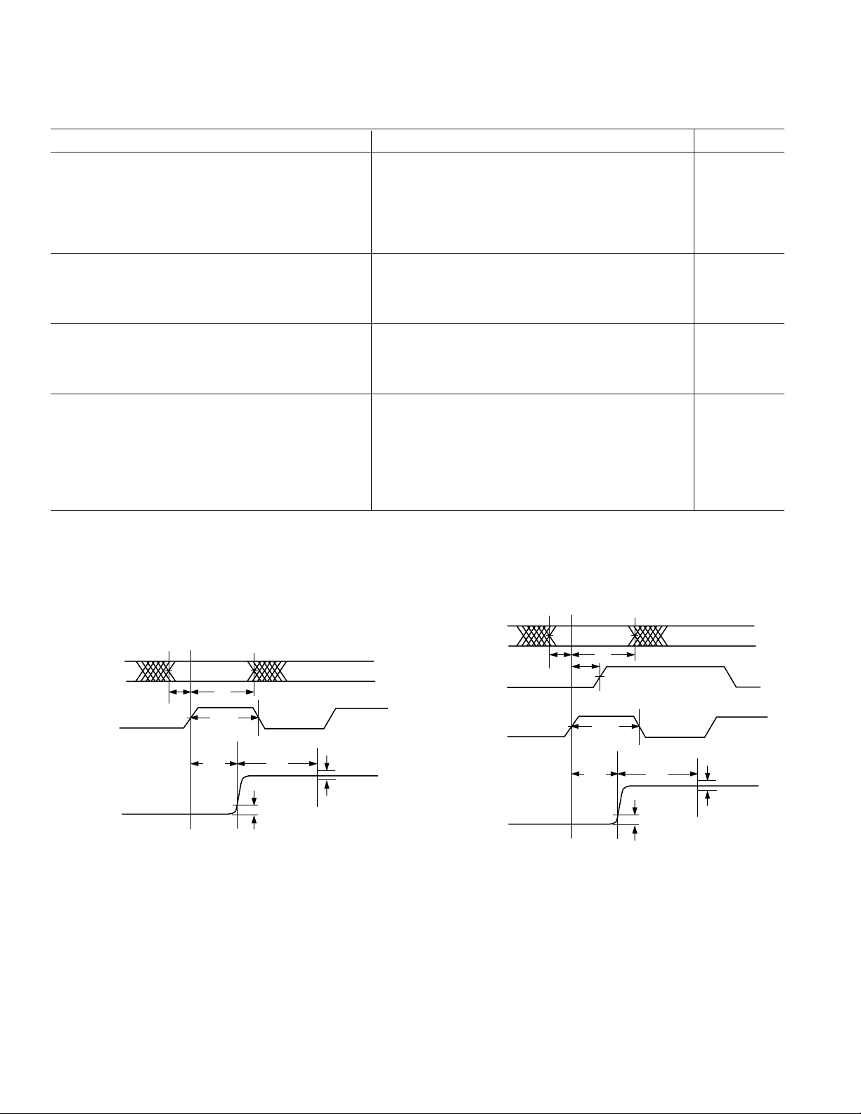
Figure 1a. Timing Diagram—PLL Clock Multiplier Enabled
Figure 1b. Timing Diagram—PLL Clock Multiplier Disabled
–4–
REV. B
AD9772A
FREQUENCY (DC TO f
DATA
)
0
–140
0
1.00.1
OUTPUT (dB)
0.2 0.3 0.4 0.5 0.6 0.7 0.8 0.9
–20
–40
–60
–80
–100
–120
TIME (Samples)
1.0
–0.4
0
5
NORMALIZED OUTPUT
10 15 20 25 30 35 40 45
0.8
0.6
0.4
0.2
0
–0.2
(T
to T
, AVDD = 3.3 V, CLKVDD = 3.3 V, PLLVDD = 0 V, DVDD = 3.3 V, I
MAX
DIGITAL FILTER SPECIFICATIONS
MIN
differential transformer-coupled output, 50 doubly terminated, unless otherwise noted.)
Parameter Min Typ Max Unit
MAXIMUM INPUT DATA RATE (f
) 150 MSPS
DATA
DIGITAL FILTER CHARACTERISTICS
Pass-Bandwidth1: 0.005 dB 0.401 f
Pass-Bandwidth: 0.01 dB 0.404 f
Pass-Bandwidth: 0.1 dB 0.422 f
Pass-Bandwidth: –3 dB 0.479 f
LINEAR PHASE (FIR IMPLEMENTATION)
STOP BAND REJECTION
0.606 f
GROUP DELAY
CLOCK
to 1.394 f
2
73 dB
CLOCK
11 Input Clocks
IMPULSE RESPONSE DURATION
–40 dB 36 Input Clocks
–60 dB 42 Input Clocks
NOTES
1
Excludes sin(x)/x characteristic of DAC.
2
Dened as the number of data clock cycles between impulse input and peak of output response.
Specications subject to change without notice.
= 20 mA,
OUTFS
OUT/fDATA
OUT/fDATA
OUT/fDATA
OUT/fDATA
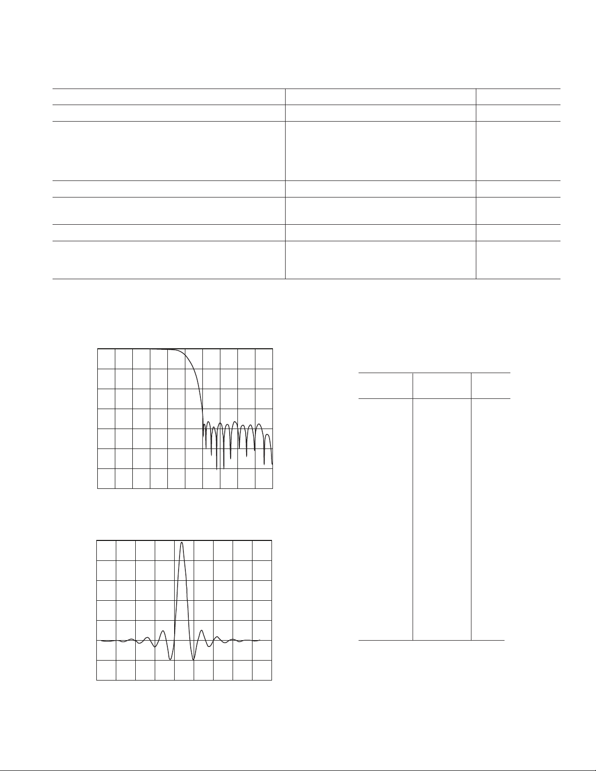
Table I. Integer Filter Coefcients for Interpolation Filter
(43-Tap Half-Band FIR Filter)
Lower Upper Integer
Coefcient Coefcient Value
H(1) H(43) 10
H(2) H(42) 0
H(3) H(41) –31
H(4) H(40) 0
H(5) H(39) 69
H(6) H(38) 0
H(7) H(37) –138
H(8) H(36) 0
H(9) H(35) 248
H(10) H(34) 0
H(11) H(33) –419
Figure 2a. FIR Filter Frequency Response—Baseband Mode
H(12) H(32) 0
H(13) H(31) 678
H(14) H(30) 0
H(15) H(29) –1083
H(16) H(28) 0
H(17) H(27) 1776
H(18) H(26) 0
H(19) H(25) –3282
H(20) H(24) 0
H(21) H(23) 10364
H(22) 16384
Figure 2b. FIR Filter Impulse Response—Baseband Mode
REV. B
–5–
AD9772A
AD9772A
–7–
REV. B
ABSOLUTE MAXIMUM RATINGS*
Parameter With Respect to Min Max Unit
AVDD, DVDD1-2, CLKVDD, PLLVDD ACOM, DCOM, CLKCOM, PLLCOM –0.3 +4.0 V
AVDD, DVDD1-2, CLKVDD, PLLVDD AVDD, DVDD1-2, CLKVDD, PLLVDD –4.0 +4.0 V
ACOM, DCOM1-2, CLKCOM, PLLCOM ACOM, DCOM1-2, CLKCOM, PLLCOM –0.3 +0.3 V
REFIO, REFLO, FSADJ, SLEEP ACOM –0.3 AVDD + 0.3 V
I
, I
OUTA
DB0–DB13, MOD0, MOD1, PLLLOCK DCOM1-2 –0.3 DVDD + 0.3 V
CLK+, CLK– CLKCOM –0.3 CLKVDD + 0.3 V
DIV0, DIV1, RESET CLKCOM –0.3 CLKVDD + 0.3 V
LPF PLLCOM –0.3 PLLVDD + 0.3 V
Junction Temperature 125 °C
Storage Temperature –65 +150 °C
Lead Temperature (10 sec) 300 °C
*Stresses above those listed under Absolute Maximum Ratings may cause permanent damage to the device. This is a stress rating only; functional operation of the device
at these or any other conditions above those indicated in the operational sections of this specication is not implied. Exposure to absolute maximum ratings for extended
periods may affect device reliability.
ACOM –1.0 AVDD + 0.3 V
OUTB
ORDERING GUIDE
Temperature Package Package
Model Range Description Option*
AD9772AAST –40°C to +85°C 48-Lead LQFP ST-48
AD9772AASTRL –40°C to +85°C 48-Lead LQFP ST-48
THERMAL CHARACTERISTIC
Thermal Resistance
48-Lead LQFP
qJA = 91°C/W
qJC = 28°C/W
AD9772A-EB Evaluation Board
*ST = Thin Plastic Quad Flatpack.
CAUTION
ESD (electrostatic discharge) sensitive device. Electrostatic charges as high as 4000 V readily accumulate
on the human body and test equipment and can discharge without detection. Although the AD9772A
features proprietary ESD protection circuitry, permanent damage may occur on devices subjected to high
energy electrostatic discharges. Therefore, proper ESD precautions are recommended to avoid performance
degradation or loss of functionality.
–6–
REV. B
36
35
34
33
32
31
30
29
28
27
26
25
13 14 15 16 17 18 19 20 21 22 23 24
1
2
3
4
5
6
7
8
9
10
11
12
48 47 46 45 44 39 38 3743 42 41 40
PIN 1
IDENTIFIER
TOP VIEW
(Not to Scale)
SLEEP
LPF
PLLVDD
PLLCOM
CLKVDD
CLKCOM
CLK–
DCOM
DCOM
(MSB) DB13
DB12
DB11
DB10
DB9
NC = NO CONNECT
DB8
DB7
DB6
DB5
CLK+
DIV0
DIV1
RESET
AD9772A
DB4
PLLLOCK
DVDD
DVDD
AVDD
AVDD
ACOM
I
OUTAIOUTB
ACOM
FSADJ
REFIO
REFLO
ACOM
DB3
DB2
DB1
(LSB) DB0
MOD0
MOD1
DCOM
DCOM
DVDD
DVDD
NC
NC
AD9772A
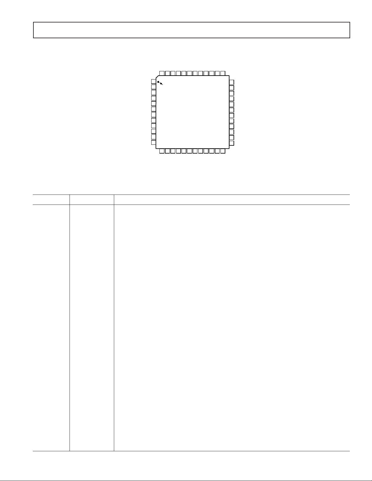
PIN CONFIGURATION
PIN FUNCTION DESCRIPTIONS
Pin No. Mnemonic Description
1, 2, 19, 20 DCOM Digital Common.
3 DB13 Most Signicant Data Bit (MSB).
4–15 DB12–DB1 Data Bits 1–12.
16 DB0 Least Signicant Data Bit (LSB).
17 MOD0 Invokes digital high-pass lter response (i. e., half-wave digital mixing mode). Active high.
18 MOD1 Invokes Zero-Stufng Mode. Active high. Note, quarter-wave digital mixing occurs with MOD0 also set high.
23, 24 NC No Connect, Leave Open.
21, 22, 47, 48 DVDD Digital Supply Voltage (3.1 V to 3.5 V).
25 PLLLOCK Phase-Lock Loop Lock Signal when PLL clock multiplier is enabled. High indicates PLL is locked to input
clock. Provides 1 clock output when PLL clock multiplier is disabled. Maximum fanout is 1 (i.e., <10 pF).
26 RESET Resets internal divider by bringing momentarily high when PLL is disabled to synchronize internal 1 clock
to the input data and/or multiple AD9772A devices.
27, 28 DIV1, DIV0 DIV1 along with DIV0 sets the PLL’s prescaler divide ratio (refer to Table III).
29 CLK+ Noninverting Input to Differential Clock. Bias to midsupply (i.e., CLKVDD/2).
30 CLK– Inverting Input to Differential Clock. Bias to midsupply (i.e., CLKVDD/2).
31 CLKCOM Clock Input Common.
32 CLKVDD Clock Input Supply Voltage (3.1 V to 3.5 V).
33 PLLCOM Phase-Lock Loop Common.
34 PLLVDD Phase-Lock Loop (PLL) Supply Voltage (3.1 V to 3.5 V). To disable PLL clock multiplier, connect PLLVDD
to PLLCOM.
35 LPF PLL Loop Filter Node. This pin should be left as a no connect (open) unless the DAC update rate is less
than 10 MSPS, in which case a series RC should be connected from LPF to PLLVDD as indicated on the
evaluation board schematic.
36 SLEEP Power-Down Control Input. Active high. Connect to ACOM if not used.
37, 41, 44 ACOM Analog Common.
38 REFLO Reference Ground when Internal 1.2 V Reference Used. Connect to AVDD to disable internal reference.
39 REFIO Reference Input/Output. Serves as reference input when internal reference disabled (i.e., tie REFLO to
AVDD). Serves as 1.2 V reference output when internal reference activated (i.e., tie REFLO to ACOM).
Requires 0.1 F capacitor to ACOM when internal reference activated.
40 FSADJ Full-Scale Current Output Adjust.
42 I
43 I
45, 46 AVDD Analog Supply Voltage (3.1 V to 3.5 V).
REV. B
–7–
Complementary DAC Current Output. Full-scale current when all data bits are 0s.
OUTB
DAC Current Output. Full-scale current when all data bits are 1s.
OUTA
AD9772A
PLLCLOCK
MULTIPLIER
EDGE-
TRIGGERED
LATCHES
2 FIR
INTERPOLATION
FILTER
AD9772A
3.3V3.3V
FROM HP8644A
SIGNAL GENERATOR
3.3V
CLKVDD
CLKCOM
CLK+
1
FILTER
CONTROL
MUX
CONTROL
MOD0
MOD1
RESET
PLLLOCK
DIV0
DIV1
PLLCOM
LPF
PLLVDD
I
OUTA
I
OUTB
REFIO
FSADJ
REFLOAVDDACOMDVDDDCOM
SLEEP
ZERO
STUFF
MUX
14-BIT DAC
100
MINI-CIRCUITS
T1–1T
20pF50
50
20pF
1.91k
0.1F
+1.2V REFERENCE
AND CONTROL AMP
AWG2021
OR
DG2020
DIGITAL
DATA
EXT.
CLOCK
HP8130
PULSE GENERATOR
CH1
CH2
EXT. INPUT
2/4
CLK–
1k
1k
1/2
CLOCK DISTRIBUTION
AND MODE SELECT
TO FSEA30
SPECTRUM
ANALYZER
DEFINITIONS OF SPECIFICATIONS
Linearity Error (Also Called Integral Nonlinearity or INL)
Linearity error is dened as the maximum deviation of the
actual analog output from the ideal output, determined by a
straight line drawn from zero to full scale.
Differential Nonlinearity (DNL)
DNL is the measure of the variation in analog value, normalized
to full scale, associated with a 1 LSB change in digital
input code.
Monotonicity
A D/A converter is monotonic if the output either increases
or remains constant as the digital input increases.
Offset Error
The deviation of the output current from the ideal of zero is
called offset error. For I
the inputs are all 0s. For I
, 0 mA output is expected when
OUTA
, 0 mA output is expected
OUTB
when all inputs are set to 1s.
Gain Error
The difference between the actual and ideal output span.
The actual span is determined by the output when all inputs
are set to 1s, minus the output when all inputs are set to 0s.
Output Compliance Range
The range of allowable voltage at the output of a currentoutput DAC. Operation beyond the maximum compliance
limits may cause either output stage saturation or breakdown,
resulting in nonlinear performance.
Temperature Drift
Temperature drift is specied as the maximum change from
the ambient (25°C) value to the value at either T
MIN
or T
MAX
For offset and gain drift, the drift is reported in ppm of fullscale range (FSR) per °C. For reference drift, the drift is
reported in ppm per °C.
Power Supply Rejection
The maximum change in the full-scale output as the supplies
are varied from minimum to maximum specied voltages.
Settling Time
The time required for the output to reach and remain within
a specied error band about its nal value, measured from
the start of the output transition.
Glitch Impulse
Asymmetrical switching times in a DAC give rise to unde
output transients that are quantied by a glitch impulse. It is
specied as the net area of the glitch in pV-s.
Spurious-Free Dynamic Range
The difference, in dB, between the rms amplitude of the output
signal and the peak spurious signal over the specied bandwidth.
Total Harmonic Distortion
THD is the ratio of the rms sum of the rst six harmonic
components to the rms value of the measured fundamental.
It is expressed as a percentage or in decibels (dB).
Signal-to-Noise Ratio (SNR)
S/N is the ratio of the rms value of the measured output
signal to the rms sum of all other spectral components below
the Nyquist frequency, excluding the rst six harmonics and
dc. The value for SNR is expressed in decibels.
Pass Band
Frequency band in which any input applied therein passes
unattenuated to the DAC output.
Stop-band Rejection
The amount of attenuation of a frequency outside the pass
band applied to the DAC, relative to a full-scale signal applied
at the DAC input within the pass band.
Group Delay
.
Number of input clocks between an impulse applied at the
device input and peak DAC output current.
Impulse Response
Response of the device to an impulse applied to the input.
Adjacent Channel Power Ratio (ACPR)
A ratio in dBc between the measured power within a channel
relative to its adjacent channel.
sired
Figure 3. Basic AC Characterization Test Setup
–8–
REV. B REV. B
Typical Performance Characteristics–AD9772A
f
OUT
(MHz)
0
–60
–100
120200
AMPLITUDE (dBm)
–40
–80
40 60 80 100
–20
OUT-OF-
BAND
IN-BAND
FREQUENCY (MHz)
0
–60
–100
1500
AMPLITUDE (dBm)
–40
–80
50 100
–20
OUT-OF-
BAND
IN-BAND
FREQUENCY (MHz)
0
–60
–100
300500
AMPLITUDE (dBm)
–40
–80
100 150 200 250
–20
OUT-OF-
BAND
IN-BAND
–12dBFS
0dBFS
–6dBFS
f
OUT
(MHz)
30150 20 25105
90
SFDR (dBc)
85
80
75
70
65
60
55
50
f
OUT
(MHz)
90
30150
SFDR (dBc)
85
80
75
70
65
60
55
50
20 25105
–12dBFS
0dBFS
35
–6dBFS
f
OUT
(MHz)
90
0
AMPLITUDE (dBm)
85
80
75
70
65
60
55
50
10 20 30 40 50 60
–12dBFS
–6dBFS
0dBFS
f
OUT
(MHz)
70
30150
SFDR (dBc)
65
60
55
50
45
40
35
30
20 25105
–12dBFS
0dBFS
–6dBFS
f
OUT
(MHz)
70
0
AMPLITUDE (dBm)
65
60
55
50
45
40
35
30
5 10 15 20 25 30 3
5
–12dBFS
–6dBFS
0dBFS
f
OUT
(MHz)
70
0
AMPLITUDE (dBm)
65
60
55
50
45
40
35
30
10 20 30 40 50 60 70
–12dBFS
–6dBFS
0dBFS
(AVDD = 3.3 V, CLKVDD = 3.3 V, PLLVDD = 0 V, DVDD = 3.3 V, I
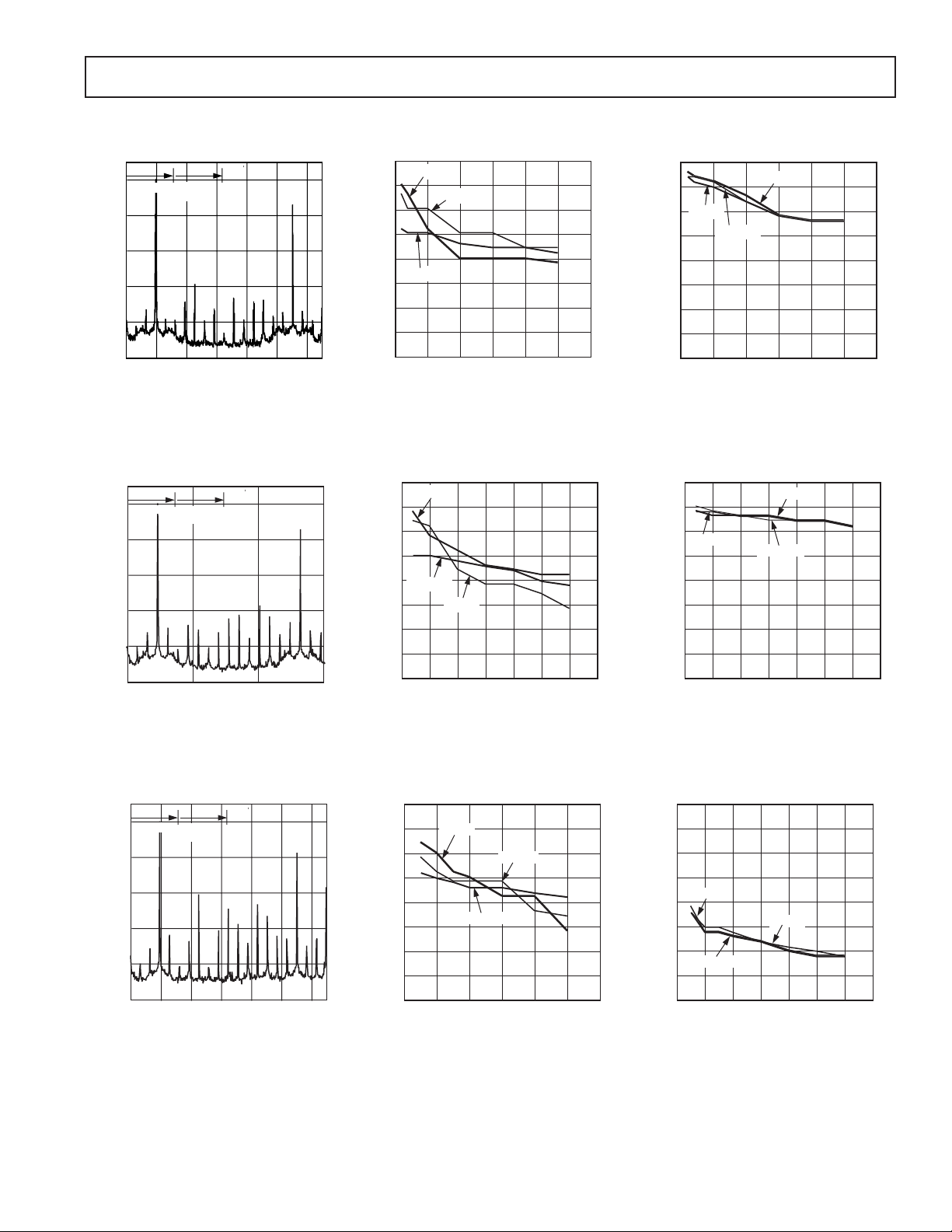
TPC 1. Single-Tone Spectral
Plot @ f
f
= f
OUT
= 65 MSPS with
DATA
/3
DATA
TPC 2. In-Band SFDR vs. f
@ f
= 20 mA. PLL disabled.)
OUTFS
= 65 MSPS
DATA
OUT
TPC 3. Out-of-Band SFDR vs.
f
OUT
@ f
= 65 MSPS
DATA
TPC 4. Single-Tone Spectral
Plot @ f
f
= f
OUT
TPC 7. Single-Tone Spectral
Plot @ f
f
= f
OUT
= 78 MSPS with
DATA
/3
DATA
= 160 MSPS with
DATA
/3
DATA
TPC 5. In-Band SFDR vs. f
@ f
= 78 MSPS
DATA
TPC 8. In-Band SFDR vs. f
@ f
= 160 MSPS
DATA
OUT
OUT
TPC 6. Out-of-Band SFDR vs.
f
OUT
@ f
= 78 MSPS
DATA
TPC 9. Out-of-Band SFDR vs.
f
OUT
@ f
= 160 MSPS
DATA
–9–
AD9772A AD9772A
f
OUT
(MHz)
90
0
IMD (dBc)
85
80
75
70
65
60
55
50
5 10 15 20 25 3
0
–3dBFS
0dBFS
–6dBFS
A
OUT
(dBFS)
90
–20
IMD (dBc)
85
80
75
70
65
60
–10 –5 0
f
DATA
= 160MSPS
f
DATA
= 65MSPS
f
DATA
= 78MSPS
–15
AVDD (Volts)
90
70
50
3.63.33.0
IMD (dBc)
80
60
85
75
65
55
3.1 3.2 3.4 3.5
–6dBFS
0dBFS
–3dBFS
f
OUT
(MHz)
90
0
IMD (dBc)
85
80
75
70
65
60
55
50
5 10 15 20 25 3
0
–3dBFS
0dBFS
–6dBFS
35
A
OUT
(dBFS)
90
–20
IMD (dBc)
85
80
75
70
65
60
–10 –5 0
f
DATA
= 160MSPS
f
DATA
= 65MSPS
f
DATA
= 78MSPS
–15
55
50
f
DAC
(MHz)
90
25
SNR (dBc)
85
80
75
70
65
60
125 175
75
55
50
PLL OFF
PLL ON, OPTIMUM DIV0/1 SETTINGS
f
OUT
(MHz)
90
0
IMD (dBc)
85
80
75
70
65
60
55
50
10 20 30 40 50 60 70
–3dBFS
0dBFS
–6dBFS
AVDD (Volts)
90
70
50
3.63.33.0
SFDR (dBc)
80
60
85
75
65
55
3.1 3.2 3.4 3.5
–6dBFS
0dBFS
–3dBFS
TEMPERATURE (C)
90
–40
SFDR (dBc)
85
80
75
70
65
60
0 8
0–20
55
50
f
DATA
= 160MSPS
f
DATA
= 78MSPS
f
DATA
= 65MSPS
20 40 60
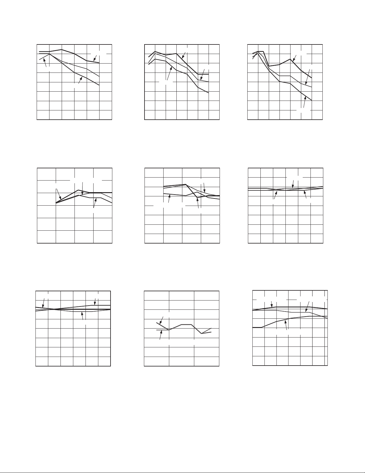
TPC 10. Third Order IMD Products vs.
f
OUT
@ f
= 65 MSPS
DATA
TPC 13. Third Order IMD Products vs.
A
OUT
@ f
OUT
= f
DAC
/11
TPC 11. Third Order IMD Products vs.
f
OUT
@ f
= 78 MSPS
DATA
TPC 14. Third Order IMD Products vs.
A
OUT
@ f
OUT
= f
DAC
/5
TPC 12. Third Order IMD Products vs.
f
@ f
OUT
TPC 15. SFDR vs. AVDD @ f
f
= 320 MSPS
DAC
= 160 MSPS
DATA
= 10 MHz,
OUT
TPC 16. Third Order IMD Products
vs. AVDD @ f
320 MSPS
= 10 MHz, f
OUT
TPC 18. In-Band SFDR vs.
Temperature @ f
OUT
= f
DATA
/11
REV. B REV. B
DAC
=
TPC 17. SNR vs. f
DAC
@ f
= 10 MHz
OUT
–10–
 Loading...