查询AD9696供应商
Ultrafast
a
FEATURES
4.5 ns Propagation Delay
200 ps Maximum Propagation Delay Dispersion
Single +5 V or 65 V Supply Operation
Complementary Matched TTL Outputs
APPLICATIONS
High Speed Line Receivers
Peak Detectors
Window Comparators
High Speed Triggers
Ultrafast Pulse Width Discriminators
GENERAL DESCRIPTION
The AD9696 and AD9698 are ultrafast TTL-compatible voltage comparators able to achieve propagation delays previously
possible only in high performance ECL devices. The AD9696 is
a single comparator providing 4.5 ns propagation delay, 200 ps
maximum delay dispersion and 1.7 ns setup time. The AD9698
is a dual comparator with equally high performance; both devices are ideal for critical timing circuits in such applications as
ATE, communications receivers and test instruments.
TTL Comparators
AD9696/AD9698
Both devices allow the use of either a single +5 V supply or
±5 V supplies. The choice of supplies determines the common
mode input voltage range available: –2.2 V to +3.7 V for ±5 V
operation, +1.4 V to +3.7 V for single +5 V supply operation.
The differential input stage features high precision, with offset
voltages that are less than 2 mV and offset currents less than
1 µA. A latch enable input is provided to allow operation in ei-
ther sample-and-hold or track-and-hold applications.
The AD9696 and AD9698 are both available as commercial
temperature range devices operating from ambient temperatures
of 0°C to +70°C, and as extended temperature range devices for
ambient temperatures from –55°C to +125°C. Both versions are
available qualified to MIL-STD-883 class B.
Package options for the AD9696 include a 10-pin TO-100 metal
can, an 8-pin ceramic DIP, an 8-pin plastic DIP, and an 8-lead
small outline plastic package. The AD9698 is available in a
16-pin ceramic DIP, a 16-lead ceramic gullwing, a 16-pin plastic
DIP and a 16-lead small outline plastic package. Military qualified versions of the AD9696 come in the TO-100 can and
ceramic DIP; the dual AD9698 comes in ceramic DIP.
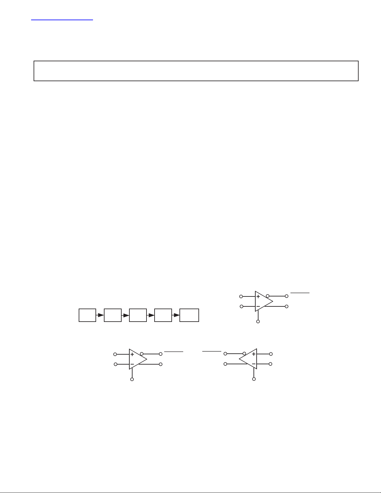
FUNCTIONAL BLOCK DIAGRAM
AD9696/AD9698 Architecture
LATCH
GAIN
LEVEL
SHIFT
OUTPUTINPUT
AD9698
NONINVERTING
INPUT
INVERTING
INPUT
#1
LATCH
ENABLE
Q OUTPUT
Q OUTPUT
REV. B
Information furnished by Analog Devices is believed to be accurate and
reliable. However, no responsibility is assumed by Analog Devices for its
use, nor for any infringements of patents or other rights of third parties
which may result from its use. No license is granted by implication or
otherwise under any patent or patent rights of Analog Devices.
AD9696
NONINVERTING
INPUT
INVERTING
INPUT
LATCH
ENABLE
Q OUTPUT
Q OUTPUT
One Technology Way, P.O. Box 9106, Norwood, MA 02062-9106, U.S.A.
Tel: 617/329-4700 World Wide Web Site: http://www.analog.com
Fax: 617/326-8703 © Analog Devices, Inc., 1997
#2
LATCH
ENABLE
Q OUTPUT
Q OUTPUT
NONINVERTING
INPUT
INVERTING
INPUT

AD9696/AD9698–SPECIFICATIONS
ABSOLUTE MAXIMUM RATINGS
1
Supply Voltage (+VS/–VS) . . . . . . . . . . . . . . . . . . . .+7 V/–7 V
Input Voltage Range . . . . . . . . . . . . . . . . . . . . . . . . . . . . ±5 V
Differential Input Voltage . . . . . . . . . . . . . . . . . . . . . . . 5.4 V
Latch Enable Voltage . . . . . . . . . . . . . . . . . . . . . –0.5 V to +V
Output Current (Continuous) . . . . . . . . . . . . . . . . . . . 20 mA
Power Dissipation . . . . . . . . . . . . . . . . . . . . . . . . . . . 600 mW
Operating Temperature Range
AD9696/AD9698KN/KQ/KR . . . . . . . . . . . . 0°C to +70°C
AD9696/AD9698TQ . . . . . . . . . . . . . . . . –55°C to +125°C
Storage Temperature Range . . . . . . . . . . . . –65°C to +150°C
Junction Temperature
S
KQ/TQ Suffixes . . . . . . . . . . . . . . . . . . . . . . . . . . . +175°C
KN/KR Suffixes . . . . . . . . . . . . . . . . . . . . . . . . . . . +150°C
2
Lead Soldering Temperature (10 sec) . . . . . . . . . . . . +300°C
(Supply Voltages = –5.2 V and +5.0 V; load as specified in Note 4,
ELECTRICAL CHARACTERISTICS
unless otherwise noted)
08C to +708C –558C to +1258C
AD9696/AD9698 AD9696/AD9698
Test KN/KQ/KR TQ
Parameter Temp Level Min Typ Max Min Typ Max Units
INPUT CHARACTERISTICS
Input Offset Voltage
4
+25°C I 1.0 2.0 1.0 2.0 mV
Full VI 3.0 3.0 mV
Input Offset Voltage Drift Full V 10 10 µV/°C
Input Bias Current +25°C I 16 55 16 55 µA
Full VI 110 110 µA
Input Offset Current +25°C I 0.4 1.0 0.4 1.0 µA
Full VI 1.3 1.3 µA
Input Capacitance +25°CV 3 3 pF
Input Voltage Range
±5.0 V Full VI –2.2 +3.7 –2.2 +3 7 V
+5.0 V Full VI +1.4 +3.7 +1.4 +3.7 V
Common Mode Rejection Ratio
±5.0 V Full VI 80 85 80 85 dB
+5.0 V Full VI 57 63 57 63 dB
LATCH ENABLE INPUT
Logic “1” Voltage Threshold Full VI 2.0 2.0 V
Logic “0” Voltage Threshold Full VI 0.8 0.8 V
Logic “1” Current Full VI 10 10 µA
Logic “0” Current Full VI 1 1 µA
DIGITAL OUTPUTS
Logic “1” Voltage (Source 4 mA) Full VI 2.7 3.5 2.7 3.5 V
Logic “0” Voltage (Sink 10 mA) Full VI 0.4 0.5 0.4 0.5 V
SWITCHING PERFORMANCE
Propagation Delay (t
PD
5
)
Input to Output HIGH Full IV 4.5 7.0 4.5 7.0 ns
Input to Output LOW Full IV 4.5 7.0 4.5 7.0 ns
Latch Enable to Output HIGH +25°C IV 6.5 8.5 6.5 8.5 ns
Latch Enable to Output LOW +25°C IV 6.5 8.5 6.5 8.5 ns
Delta Delay Between Outputs +25°C IV 0.5 1.5 0.5 1.5 ns
Propagation Delay Dispersion
20 mV to 100 mV Overdrive +25°C V 100 100 ps
100 mV to 1.0 V Overdrive +25°C IV 100 200 100 200 ps
Rise Time
Fall Time
10
10
+25°C V 1.85 1.85 ns
+25°C V 1.35 1.35 ns
Latch Enable
Pulse Width [t
Setup Time (t
] +25°C IV 3.5 2.5 3.5 2.5 ns
PW(E)
) +25°C IV 3 1.7 3 1.7 ns
S
Hold Time (tH) +25°C IV 3 1.9 3 1.9 ns
–2–
REV. B

AD9696/AD9698
08C to +708C –558C to +1258C
AD9696/AD9698 AD9696/AD9698
Test KN/KQ/KR TQ
Parameter Temp Level Min Typ Max Min Typ Max Units
POWER SUPPLY
Positive Supply Current
AD9696 Full VI 26 32 26 32 mA
AD9698 Full VI 52 64 52 64 mA
Negative Supply Current
AD9696 Full VI 2.5 4.0 2.5 4.0 mA
AD9698 Full VI 5.0 8.0 5.0 8.0 mA
Power Dissipation
AD9696 +5.0 V Full V 130 130 mW
AD9696 ±5.0 V Full V 146 146 mW
AD9698 +5.0 V Full V 260 260 mW
AD9698 ±5.0 V Full V 292 292 mW
Power Supply Rejection Ratio
NOTES
1
Absolute maximum ratings are limiting values, to be applied individually,
and beyond which the serviceability of the circuit may be impaired. Functional
operability is not necessarily implied. Exposure to absolute maximum rating
conditions for an extended period of time may affect device reliability.
2
Typical thermal impedances:
AD9696 Metal Can θJA = 170°C/W θJC = 50°C/W
AD9696 Ceramic DIP θJA = 110°C/W θJC = 20°C/W
AD9696 Plastic DIP θJA = 160°C/W θJC = 30°C/W
AD9696 Plastic SOIC θJA = 180°C/W θJC = 30°C/W
AD9698 Ceramic DIP θJA = 90°C/W θJC = 25°C/W
AD9698 Plastic DIP θJA = 100°C/W θJC = 20°C/W
AD9698 Plastic SOIC θJA = 120°C/W θJC = 20°C/W
6
7
8
9
+25°CVI 70 70 dB
(+5.0 V)
(–5.2 V)
Full VI 65 65 dB
3
Load circuit has 420 Ω from +VS to output; 460 Ω from output to ground.
4
RS ≤100 Ω.
5
Propagation delays measured with 100 mV pulse; 10 mV overdrive.
6
Supply voltages should remain stable within ±5% for normal operation.
7
Specification applies to both +5 V and ±5 V supply operation.
8
Specification applies to only ±5 V supply operation.
9
Measured with nominal values ±5% of +VS and –VS.
10
Although fall time is faster than rise time, the complementary outputs cross at
midpoint of logic swing because of delay on start of falling edge.
Specifications subject to change without notice.
EXPLANATION OF TEST LEVELS
Test Level
I – 100% production tested.
II – 100% production tested at +25°C, and sample tested at
specified temperatures.
III – Sample tested only.
IV – Parameter is guaranteed by design and characterization
testing.
V – Parameter is a typical value only.
VI – All devices are 100% production tested at +25°C.
100% production tested at temperature extremes for
extended temperature devices; sample tested at temp-
erature extremes for commercial/industrial devices.
ORDERING GUIDE
Package
Model Package Temperature Option
1
AD9696KN Plastic DIP 0°C to +70°C N-8
AD9696KR SOIC 0°C to +70°C R-8
AD9696KQ Cerdip 0°C to +70°C Q-8
AD9696TQ Cerdip –55°C to +125°C Q-8
AD9696TZ/883B
2
Gullwing –55°C to +125°C Z-8A
AD9698KN Plastic DIP 0°C to +70°C N-16
AD9698KR SOIC 0°C to +70°C R-16A
AD9698KQ Cerdip 0°C to +70°C Q-16
AD9698TQ Cerdip –55°C to +125°C Q-16
AD9698TZ/883B3Gullwing –55°C to +125°C Z-16
NOTES
1
N = Plastic DIP, Q = Cerdip, R = Small Outline (SOIC), Z = Ceramic Leaded
Chip Carrier.
2
Refer to AD9696TZ/883B military data sheet.
3
Refer to AD9698TZ/883B military data sheet.
REV. B
–3–
 Loading...