ANALOG DEVICES AD9662 Service Manual

3-Channel Laser Diode Driver
FEATURES
Current-controlled current source
with 3 input channels
Output current for Channel 3—315 mA
Output current for other channels—210 mA
Rise time/fall time of 0.8 ns
On-chip oscillator
Single 5 V power supply (±10%)
Low output overshoot
Low power consumption
APPLICATIONS
CD-RW drives
DVD-RW, DVD+RW, MO drives
Laser diode current switching
GENERAL DESCRIPTION
The AD9662 is a laser diode driver for high performance CD
and DVD recordable drives. It includes three channels for three
different optical power levels: the read channel generates a
continuous output power level, whereas Channel 2 and
Channel 3 are used as write channels having 0.8 ns rise/fall
times. All channel currents are summed at the I
channel’s output current is established by multiplying the
channel’s gain by the channel’s input current. The input current
for each of the input channels—INR, IN2, and IN3—can be set
either by using an external resistor that converts an input
voltage to a current or by directly using a current source.
pin. Each
OUT
with Oscillator
FUNCTIONAL BLOCK DIAGRAM
IN3
OUTEN3
IN2
OUTEN2
INR
OUTENR
OSCEN
CHANNEL 3
CHANNEL 2
READ CHANNEL
OSCILLATOR
R
R
S
F
Figure 1. AD9662 3-Channel Laser Diode Driver
AD9662
OUTPUT
ENABLE
I
OUT
04389-0-001
An on-chip oscillator is provided to allow output current
modulation (to reduce laser mode hopping). Two external
resistors control the frequency and the amplitude swing of the
oscillator. The push-pull oscillator can swing up to 100 mA p-p
and has a frequency range of 200 MHz to 500 MHz.
Rev. C
Information furnished by Analog Devices is believed to be accurate and reliable. However, no
responsibility is assumed by Anal og Devices for its use, nor for any infringements of patents or ot her
rights of third parties that may result from its use. Specifications subject to change without notice. No
license is granted by implication or otherwise under any patent or patent rights of Analog Devices.
Trademarks and registered trademarks are the property of their respective owners.
One Technology Way, P.O. Box 9106, Norwood, MA 02062-9106, U.S.A.
Tel: 781.329.4700 www.analog.com
Fax: 781.461.3113 © 2005 Analog Devices, Inc. All rights reserved.

AD9662
TABLE OF CONTENTS
Features .............................................................................................. 1
Pin Configuration and Function Descriptions..............................6
Applications....................................................................................... 1
General Description......................................................................... 1
Functional Block Diagram .............................................................. 1
Revision History ............................................................................... 2
Specifications..................................................................................... 3
Absolute Maximum Ratings............................................................ 5
ESD Caution.................................................................................. 5
REVISION HISTORY
11/05—Rev. SpB to Rev. C
Changes to Format ............................................................. Universal
7/04—Rev. Sp0 to Rev. SpB
Changes to Note 2 in Specifications............................................... 4
Changes to Absolute Maximum Ratings....................................... 5
Changes to Figure 17...................................................................... 12
12/03—Rev. SpA: Initial 2-Page Web Version
Typical Perf or m an c e Character i st ic s ..............................................7
Applications..................................................................................... 10
Temperature Considerations .................................................... 10
Evaluation Board ............................................................................ 12
Outline Dimensions ....................................................................... 13
Ordering Guide .......................................................................... 13
12/03—Rev. Sp0: Initial Full Version
Rev. C | Page 2 of 16

AD9662
SPECIFICATIONS
At T
, VCC = 5 V, ENABLE = 1, OSCEN = 0,
AMB
Table 1.
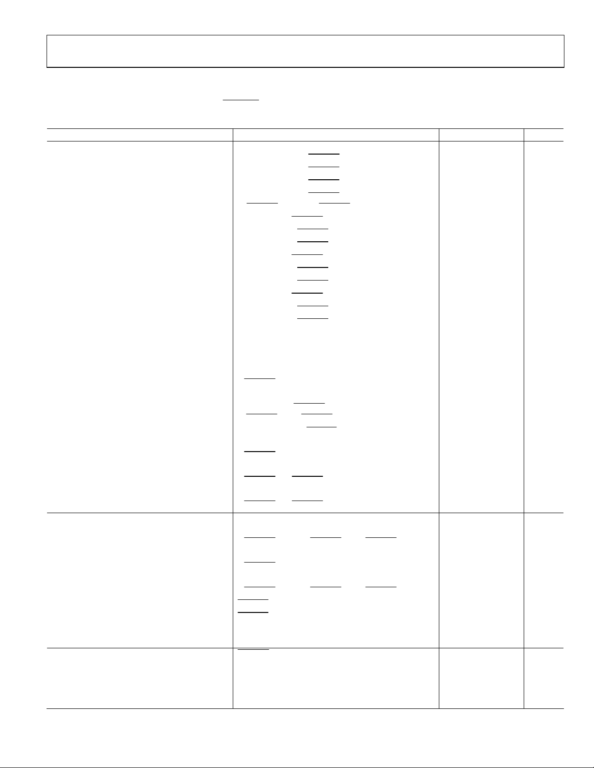
Parameter Conditions Min Typ Max Unit
LASER AMPLIFIER
Output Current Read Channel
Output Current Channel 2
Output Current Channel 3
Total Output Current
Output Current Linearity
Output Current Linearity
Output Current Linearity
Best-Fit Current Gain
Best-Fit Current Gain
Best-Fit Current Gain
Best-Fit Current Offset
Best-Fit Current Offset
Best-Fit Current Offset
I
Series Resistance Total R
OUT
1
1
1
1
1
1
1
1
1
Input Impedance (RIN), Channel R, Channel 2 RIN to GND 160 200 240 Ω
Input Impedance (RIN), Channel 3 RIN to GND 80 100 120 Ω
I
Supply Sensitivity (PSRR) I
OUT
Read Mode
I
Supply Sensitivity (PSRR) I
OUT
Write Mode
Output Current Noise
I
Temperature Sensitivity I
OUT
Read Mode
I
Temperature Sensitivity I
OUT
Write Mode Channel 2
I
Temperature Sensitivity I
OUT
Write Mode Channel 3
LASER AMPLIFIER AC SPECIFICATIONS
Write Rise Time
2
Write Fall Time
2
Output Current Overshoot I
I
ON Propagation Delay
OUT
I
OFF Propagation Delay
OUT
Disable Time ENABLE 50% H-L to I
Enable Time ENABLE 50% L-H to I
OSCILLATOR SPECIFICATIONS
Oscillator Frequency RF = 9.53 kΩ, RS = 23.7 kΩ 265 300 325 MHz
Oscillator Frequency Temperature Coefficient RF = 9.53 kΩ, RS = 23.7 kΩ 600 ppm/°C
Disable Time Oscillator OSCEN 50% H-L to amplitude at 50% of initial value 4 ns
Enable Time Oscillator OSCEN 50% L-H to amplitude at 50% of final value 6 ns
OUTENx
= 1, unless otherwise stated.
Output is sourcing,
Output is sourcing,
Output is sourcing,
Output is sourcing,
OUTENR
(
= 0 and/or
Read Channel,
Write2 Channel,
Write3 Channel,
Read Channel,
Write2 Channel,
Write3 Channel,
Read Channel,
Write2 Channel,
Write3 Channel,
to VCC rail 6.5 10 Ω
OUT
= 50 mA (read-only), VCC = 5 V ± 10% 10 15 %/V
OUT
OUTENR
OUT
= 0
= 100 mA (50 mA read, 50 mA write) 10 15 %/V
VCC = 5 V ± 10%,
OUTEN2
(
I
OUT
OUT
OUTENR
OUT
OUTENR
OUT
OUTENR
I
OUT
OUTENR
I
OUT
OUTENR
OUT
OUTENR
OUTENx
OUTENx
OUTENR
= 0 or
= 50 mA (Read),
= 50 mA (read-only) 100 ppm/°C
= 0
= 100 mA (50 mA Read, 50 mA Write2) 100 ppm/°C
= 0,
= 100 mA (50 mA Read, 50 mA Write3) 100 ppm/°C
= 0,
= 50 mA dc (Read), 50 mA pulse W2 or W3 0.8 1.8 ns
= 0 and (
= 50 mA dc (Read), 50 mA pulse W2 or W3 0.6 1.8 ns
= 0
= 50 mA dc (Read), 50 mA pulse W2 or W3 13 %
= 0 and (
50% H-L to I
50% L-H to I
= 0
OUTENR
OUTEN2
OUTEN3
OUTEN3
OUTENR
OUTEN2
OUTEN3
OUTENR
OUTEN2
OUTEN3
OUTENR
OUTEN2
OUTEN3
OUTENR
OUTEN3
OUTENR
OUTEN2
OUTEN3
OUTEN2
OUTEN2
OUT
OUT
OUT
OUT
= 0
= 0
= 0
= 0 and
OUTEN2
= 0)
= 0
= 0
= 0
= 0
= 0
= 0
= 0
= 0
= 0
= 0 and
= 0)
= 0, f = 300 MHz
= 0
= 0
OUTEN3
= 0 or
= 0 or
OUTEN3
= 0)
= 0)
at 50% of final value
at 50% of initial value
at 50% of initial value 5.4 ns
at 50% of final value 13.5 ns
210 235 mA
210 235 mA
315 340 mA
>550 mA
−4 ±0.6 +4 %
−4 ±0.6 +4 %
−4 ±0.1 +4 %
125 135 145 mA/mA
120 130 140 mA/mA
240 260 280 mA/mA
−7 ±0.6 +7 mA
−7 ±0.6 +7 mA
−30 −2 +15 mA
150 pA/√Hz
2.7 ns
2.7 ns
Rev. C | Page 3 of 16

AD9662
Parameter Conditions Min Typ Max Unit
LOGIC SPECIFICATIONS
Logic HI Threshold 2.0 V
Logic LO Threshold 0.8 V
Input Impedance
Input Leakage Current
SUPPLY CURRENT ENABLE OSCEN
OUTENx
OUTENx
, ENABLE, OSCEN
, ENABLE, OSCEN
OUTENR OUTEN2 OUTEN3
Power-Down 0 0 1 1 1 8.5 10 mA
Power-Up
Inputs Disabled 1 0 1 1 1 18 22 mA
Inputs Disabled, OSC Enabled 1 1 1 1 1 52 62 mA
Read Mode, OSC Enabled
I
= 50 mA
OUT
Write Mode
I
OUT
3
= 100 mA (50 mA W2, 50 mA W3)
3
1 1 0 1 1 55 65 mA
1 0 1 0 0 29 35 mA
OPERATING CONDITIONS
Supply Voltage Range 4.5 5.5 V
Operating Temperature Range 0 85 °C
1
Output linearity, offset current, and gain are calculated using a best-fit method at 30 mA, 45 mA, 60 mA, 75 mA, and 90 mA for the Read and Write2 Channels and
90 mA, 105 mA, 120 mA, 135 mA, and 150 mA for Write Channel 3. Each channel’s output current is given by I
2
This parameter is guaranteed by design and characterization using six sigma. Rise and fall times are measured electrically from the 10% to 90% points using a Sharp
GH0781JA2C diode as a load.
3
The values specified do not include the output current.
= (IIN × Gain) + IOS.
OUT
>10 MΩ
<1 μA
Rev. C | Page 4 of 16

AD9662
ABSOLUTE MAXIMUM RATINGS
Table 2.
Parameter Range
Supply Voltage +V
Pin 9, Pin 15, and Pin 16 5.5 V
Input Pins
Pin 1 and Pin 2 2.2 mA
Pin 5 1.6 mA
Pin 6, Pin 7, Pin 8, Pin 10, and Pin 11 −0.8 V to +5.5 V
Internal Power Dissipation
16-Lead QSOP 620 mW
Operating Temperature Range 0°C to +85°C
Storage Temperature Range −65°C to +150°C
Lead Temperature, Soldering 60 sec 300°C
1
Power dissipation is specified on SEMI standard 4-layer board.
S
1
Stresses above those listed under Absolute Maximum Ratings
may cause permanent damage to the device. This is a stress
rating only; functional operation of the device at these or any
other conditions above those indicated in the operational
section of this specification is not implied. Exposure to absolute
maximum rating conditions for extended periods may affect
device reliability.
ESD CAUTION
ESD (electrostatic discharge) sensitive device. Electrostatic charges as high as 4000 V readily accumulate on the
human body and test equipment and can discharge without detection. Although this product features
proprietary ESD protection circuitry, permanent damage may occur on devices subjected to high energy
electrostatic discharges. Therefore, proper ESD precautions are recommended to avoid performance
degradation or loss of functionality.
Rev. C | Page 5 of 16
 Loading...