Analog Devices AD9661AKR-REEL, AD9661AKR Datasheet

Laser Diode Driver
a
FEATURES
< 2 ns Rise/Fall Times
Output Current: 120 mA
Single +5 V Power Supply
Switching Rate: 200 MHz typ
Onboard Light Power Control Loop
APPLICATIONS
Laser Printers and Copiers
GENERAL DESCRIPTION
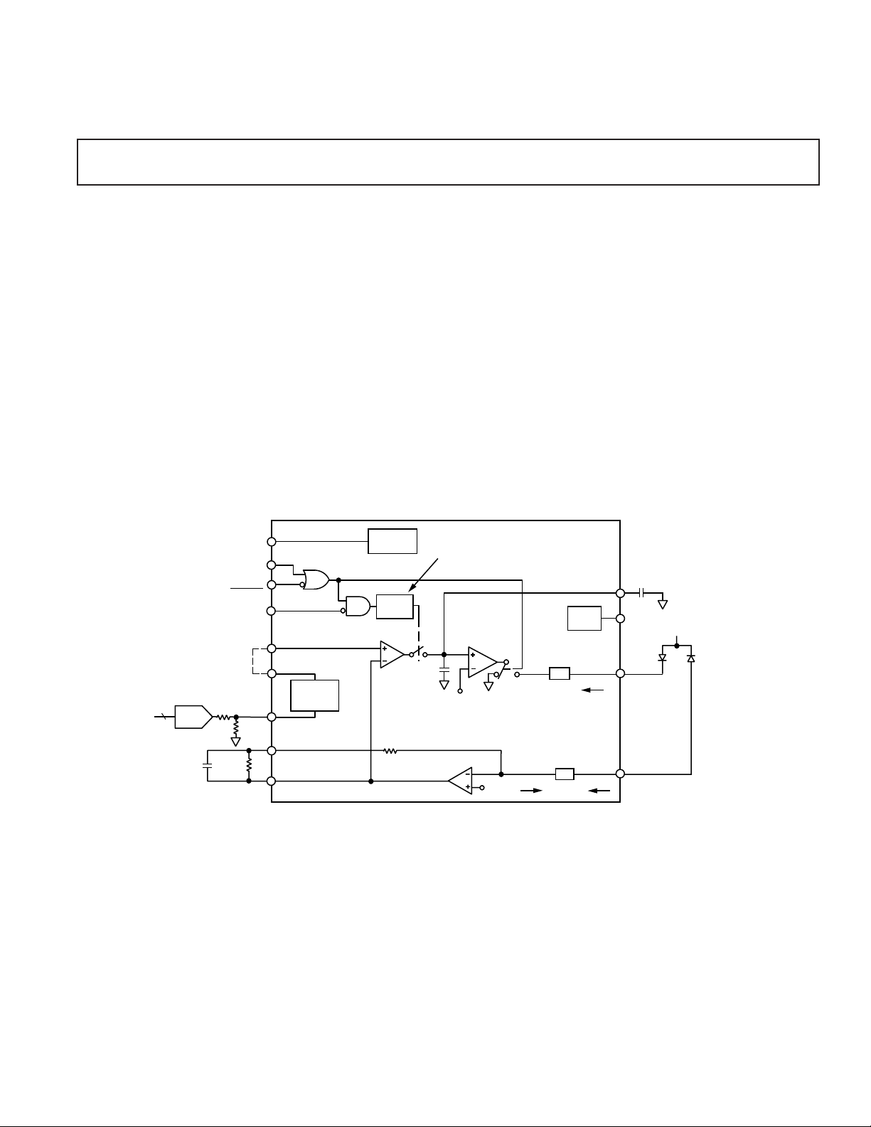
The AD9661A is a highly integrated driver for laser diode applications such as printers and copiers. The AD9661A gets feedback from an external photo detector and includes an analog
feedback loop to allow users to set the power level of the laser,
and switch the laser on and off at up to 100 MHz. Output rise
FUNCTIONAL BLOCK DIAGRAM
with Light Power Control
AD9661A
and fall times are 2 ns to complement printer applications that
use image enhancing techniques such as pulse width modulation to achieve gray scale and resolution enhancement. Control
signals are TTL/CMOS compatible.
The driver output provides up to 120 mA of current into an
infrared N type laser, and the onboard disable circuit turns off
the output driver and returns the light power control loop to a
safe state.
The AD9661A can also be used in closed-loop applications in
which the output power level follows an analog POWER LEVEL
voltage input. By optimizing the external hold capacitor and
the photo detector, the loop can achieve bandwidths as high as
25 MHz.
The AD9661A is offered in a 28-pin plastic SOIC for
operation over the commercial temperature range (0°C to
+70°C).
PULSE
CAL
LEVEL
GAIN
TTL
TTL
TTL
TTL
ANALOGPOWER
V
LEVEL SHIFT IN
LEVEL
SHIFT
CIRCUIT
0–1.6V
ANALOG
DISABLE
PULSE2
LEVEL
LEVEL
SHIFT OUT
8
DAC
C
GAIN
SHIFT IN
R
GAIN
POWER
MONITOR
DISABLE
CIRCUIT
*
DELAY
+ V
REF
*13ns DELAY ON RISING
EDGE; 0ns ON FALLING
5pF
V1
REF
1:10
VOLT
REF
3–120mA
I
OUT
HOLD
V
REF
LASER
DIODE
OUTPUT
+5V
PHOTO
DETECTOR
AD9661A
50Ω
1:1
I
MONITOR
V
REF
I
MONITOR
SENSE IN
1.0V
REV. 0
Information furnished by Analog Devices is believed to be accurate and
reliable. However, no responsibility is assumed by Analog Devices for its
use, nor for any infringements of patents or other rights of third parties
which may result from its use. No license is granted by implication or
otherwise under any patent or patent rights of Analog Devices.
© Analog Devices, Inc., 1995
One Technology Way, P.O. Box 9106, Norwood, MA 02062-9106, U.S.A.
Tel: 617/329-4700 Fax: 617/326-8703

AD9661A–SPECIFICA TIONS
(+VS = +5 V, Temperature = +258C unless otherwise noted)
Test AD9661AKR
Parameter Level Temp Min Typ Max Units Conditions
ANALOG INPUT
Input Voltage Range, POWER LEVEL IV Full V
Input Bias Current, POWER LEVEL I +25°C –50 +50 µA
Analog Bandwidth, Control Loop
1
V +25°C 25 MHz C
REF
V
REF
+ 1.6 V
= 33 pF, RF = 1 kΩ, CF = 2 pF
HOLD
Input Voltage Range, LEVEL SHIFT IN IV Full 0.1 1.6 V
Input Bias Current, LEVEL SHIFT IN I +25°C –10 0 µA
Analog Bandwidth, Level Shift
2
V Full 130 MHz
Level Shift Offset I +25°C –32 +32 mV
Level Shift Gain I +25°C 0.95 1.0 1.05 V/V
OUTPUTS
Output Current, I
OUT
I +25°C 120 mA V
OUT
= 2.5 V
Output Compliance Range IV +25°C 2.50 5.25 V
Idle Current I +25°C 2 5.0 mA PULSE = LOW, DISABLE = LOW
Disable Current IV +25°C 1.0 µA PULSE = LOW, DISABLE = HIGH
SWITCHING PERFORMANCE
Maximum Pulse Rate V +25°C 200 MHz Output Current –3 dB
Output Propagation Delay (tPD), Rising3IV Full 2.9 3.9 5.0 ns
Output Propagation Delay (tPD), Falling3IV Full 3.2 3.7 4.3 ns
Output Current Rise Time
Output Current Fall Time
CAL Aperture Delay
Disable Time
7
4
5
6
IV Full 1.5 2.0 ns
IV Full 1.5 2.0 ns
IV Full 13 ns
IV +25°C35ns
HOLD NODE
Input Bias Current I +25°C –200 200 nA V
Input Voltage Range IV Full V
REF
V
+ 1.6 V Open-Loop Application Only
REF
HOLD
= 2.5 V
Minimum External Hold Cap V Full 25 pF
TTL/CMOS INPUTS
8
Logic “1” Voltage I +25°C 2.0 V
Logic “1” Voltage IV Full 2.0 V
Logic “0” Voltage I +25°C 0.8 V
Logic “0” Voltage IV Full 0.8 V
Logic “1” Current I +25°C –10 10 µAV
Logic “0” Current I +25°C –1.5 mA V
HIGH
LOW
= 5.0 V
= 0.8 V
BANDGAP REFERENCE
Output Voltage (V
) I +25°C 1.6 1.8 1.9 V
REF
Temperature Coefficient V +25°C –0.1 mV/°C
Output Current V +25°C –0.5 1.0 mA
SENSE IN
Current Gain I +25°C 0.95 1 1.02 mA/mA
Voltage I +25°C 0.7 1.0 1.3 V
Input Resistance V +25°C <150 Ω
POWER SUPPLY
+VS Voltage I +25°C 4.75 5.00 5.25 V
+VS Current I +25°C 60 75 95 mA DISABLE = HIGH, V
HOLD
= V
REF
,
VS = 5.0 V
NOTES
1
Based on rise time of closed-loop pulse response. See Performance Curves.
2
Based on rise time of pulse response.
3
Propagation delay measured from the 50% of the rising/falling transition of WRITE PULSE to the 50% point of the rising/falling edge of the output modulation
current.
4
Rise time measured between the 10% and 90% points of the rising transition of the modulation current.
5
Fall time measured between the 10% and 90% points of the falling transition of the modulation current.
6
Aperture Delay is measured from the 50% point of the rising edge of WRITE PULSE to the time when the output modulation begins to recalibrate, WRITE CAL is
held during this test.
7
Disable Time is measured from the 50% point of the rising edge of DISABLE to the 50% point of the falling transition of the output current. Fall time during disable
is similar to fall time during normal operation.
8
PULSE, PULSE2, DISABLE, and CAL are TTL/CMOS compatible inputs.
Specifications subject to change without notice.
–2–
REV. 0

AD9661A
ABSOLUTE MAXIMUM RATINGS*
+VS . . . . . . . . . . . . . . . . . . . . . . . . . . . . . . . . . . . . . . . . . +6 V
POWER LEVEL, LEVEL SHIFT IN . . . . . . . . . . . 0 V to +V
TTL/CMOS INPUTS . . . . . . . . . . . . . . . . . . . . –0.5 V to +V
S
S
Output Current . . . . . . . . . . . . . . . . . . . . . . . . . . . . . . 200 mA
Operating Temperature
AD9661AKR . . . . . . . . . . . . . . . . . . . . . . . . . 0°C to +70°C
Storage Temperature . . . . . . . . . . . . . . . . . . –65°C to +150°C
Maximum Junction Temperature . . . . . . . . . . . . . . . . . +150°C
Lead Soldering Temp (10 sec) . . . . . . . . . . . . . . . . . . . +300°C
*Absolute maximum ratings are limiting values, to be applied individually, and
beyond which the serviceability of the circuit may be impaired. Functional
operability under any of these conditions is not necessarily implied. Exposure of
absolute maximum rating conditions for extended periods of time may affect
device reliability.
ORDERING GUIDE
Model Temperature Range Package Option
AD9661AKR 0°C to +70°C R-28
AD9661AKR-REEL 0°C to +70°C R-28 (1000/Reel)
+V
SENSE
1mA
IN
S
1mA
TTL
INPUT
+V
S
EXPLANATION OF TEST LEVELS
Test Level
I – 100% production tested.
II – 100% production tested at +25°C, and sample tested at
specified temperatures.
III – Sample tested only.
IV – Parameter is guaranteed by design and characterization
testing.
V – Parameter is a typical value only.
VI – All devices are 100% production tested at +25°C; 100%
production tested at temperature extremes for military
devices; sample tested at temperature extremes for
commercial/industrial devices.
+V
S
V
BANDGAP
100Ω
V
REF
450Ω
50Ω 50Ω
OUTPUT
HOLD
T/H
1250Ω
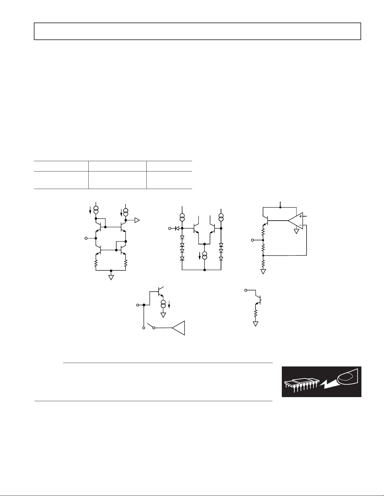
Equivalent Circuits
CAUTION
ESD (electrostatic discharge) sensitive device. Electrostatic charges as high as 4000 V readily
accumulate on the human body and test equipment and can discharge without detection.
Although the AD9661A features proprietary ESD protection circuitry, permanent damage may
occur on devices subjected to high energy electrostatic discharges. Therefore, proper ESD
precautions are recommended to avoid performance degradation or loss of functionality.
WARNING!
ESD SENSITIVE DEVICE
REV. 0
–3–

AD9661A
Pin Function
PIN DESCRIPTIONS
OUTPUT Analog laser diode current output. Connect to cathode of laser diode, anode connected to +V
to V
POWER LEVEL Analog voltage input, V
during calibration as follows:
REF
+ 1.6 V. Output current is set proportional to the POWER LEVEL
REF
I
MONITOR
V
POWER LEVEL
=
R
GAIN
–V
+ 50 Ω
REF
externally.
S
CAL TTL/CMOS compatible, feedback loop T/H control signal. Logic LOW enables calibration mode, and
the feedback loop T/H goes into track mode 13 ns after (the aperture delay) PULSE goes logic HIGH
(there is no aperture delay if PULSE goes high before CAL transitions to a LOW level). Logic HIGH disables the T/H and immediately places it in hold mode. PULSE should be held HIGH while calibrating.
Floats logic HIGH.
HOLD External hold capacitor for the bias loop T/H. Approximate droop in the output current while CAL is
logic HIGH is:
±∆I
OUT
18 ×10
=
Bandwidth of the loop is:
BW ≈
PULSE TTL/CMOS compatible, current control signal. Logic HIGH supplies I
LOW turns I
PULSE 2 TTL/CMOS compatible, current control signal. Logic LOW supplies I
HIGH turns I
SENSE IN Analog current input, I
anode of the PIN diode, with the PIN cathode connected to +V
off. Floats logic HIGH.
OUT
off. Floats logic HIGH.
OUT
MONITOR
–9
t
HOLD
C
HOLD
1
2 π(550 Ω)C
, from PIN photo detector diode. SENSE IN should be connected to the
HOLD
to the laser diode. Logic
OUT
to the laser diode. Logic
OUT
or another positive voltage. Voltage at
S
SENSE IN varies slightly with temperature and current, but is typically 1.0 V.
GAIN External connection for the feedback network of the transimpedance amplifier. External feedback network,
R
GAIN
and C
, should be connected between GAIN and POWER MONITOR. See text for choosing
GAIN
values.
POWER MONITOR Output voltage monitor of the internal feedback loop. Voltage is proportional to feedback current from
photo diode, I
MONITOR
.
DISABLE TTL/CMOS compatible, current output disable circuit. Logic LOW for normal operation; logic HIGH
disables the current outputs to the laser diode, and drives the voltage on the hold capacitors close to V
REF
(minimizes the output current when the device is re-enabled). DISABLE floats logic HIGH.
V
+V
REF
S
Analog Voltage output, internal bandgap voltage reference, ~1.8 V, provided to user for power level offset.
Power Supply, nominally +5 V. All +VS connections should be tied together externally.
GROUND Ground reference. All GROUND connections should be tied together externally.
LEVEL SHIFT IN Analog input to the on board level shift circuit. Input Range 0.1 V – 1.6 V.
LEVEL SHIFT OUT Voltage output from on board level shift circuit. Connect to POWER LEVEL externally to use the on
board level shift circuit. Output voltage is V
LEVEL SHIFT OUT
= V
LEVEL SHIFT IN
+V
REF
.
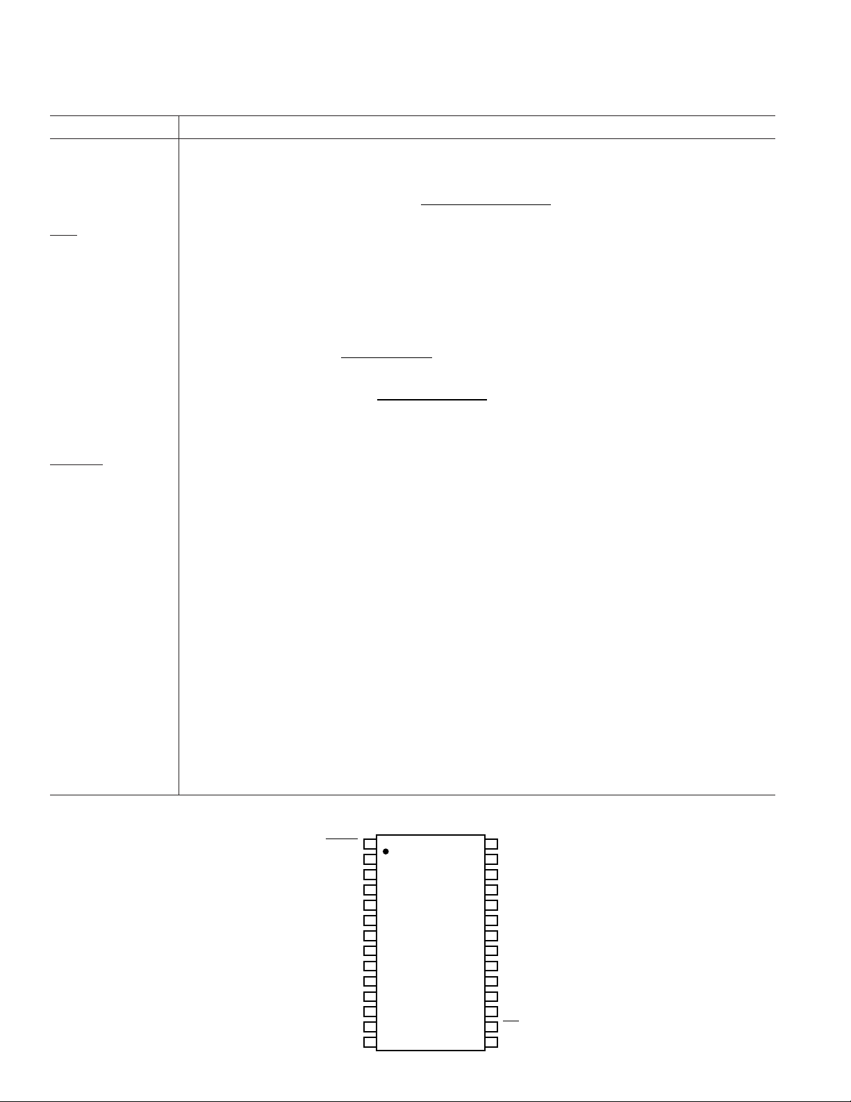
PIN ASSIGNMENTS
PULSE2
DNC
V
REF
LEVEL SHIFT IN
GAIN
POWER MONITOR
SENSE INPUT
GROUND
+V
GROUND
HOLD
POWER LEVEL
LEVEL SHIFT OUT
DISABLE
1
2
3
4
5
6
AD9661AKR
7
(Not to Scale)
8
9
S
10
11
12
13
14
–4–
28
27
26
25
24
23
22
21
20
19
18
17
16
15
+V
S
GROUND
OUTPUT
GROUND
OUTPUT
GROUND
OUTPUT
GROUND
OUTPUT
GROUND
+V
S
GROUND
CAL
PULSE1
REV. 0
