

Laser Diode Driver
a
FEATURES
< 2 ns Rise/Fall Times
Output Current: 120 mA
Single +5 V Power Supply
Switching Rate: 200 MHz typ
Onboard Light Power Control Loop
APPLICATIONS
Laser Printers and Copiers
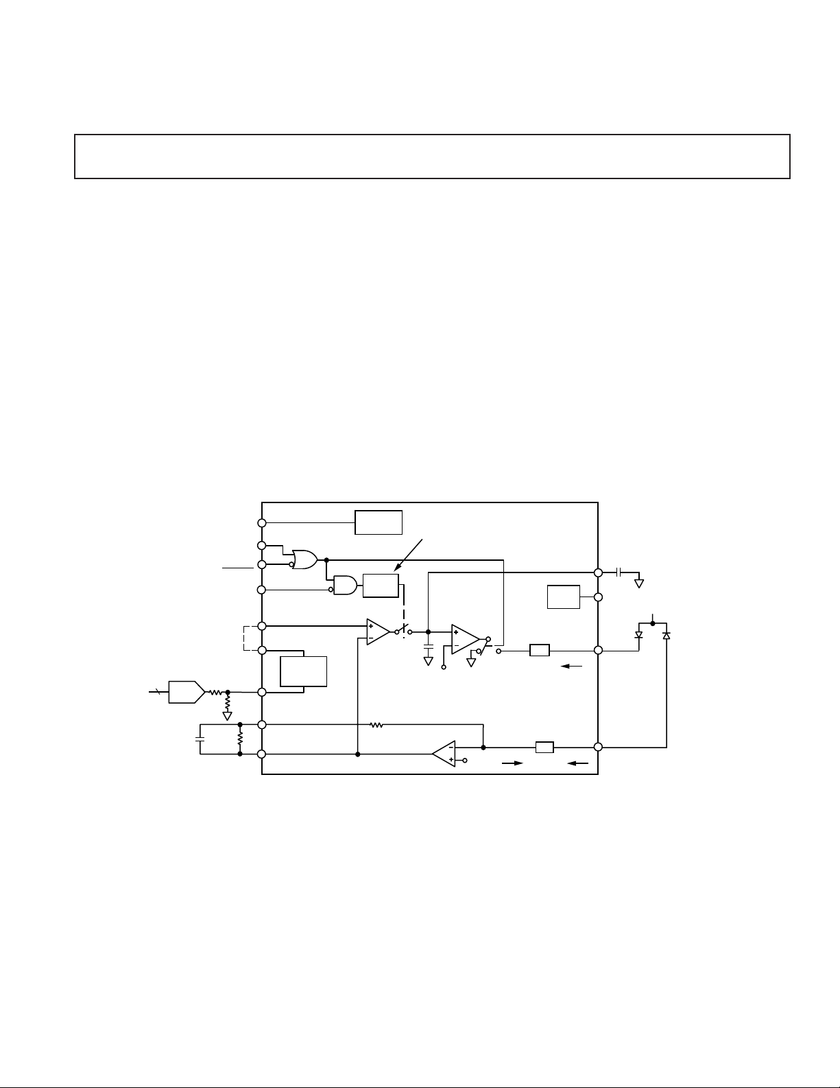
GENERAL DESCRIPTION
The AD9661A is a highly integrated driver for laser diode applications such as printers and copiers. The AD9661A gets feedback from an external photo detector and includes an analog
feedback loop to allow users to set the power level of the laser,
and switch the laser on and off at up to 100 MHz. Output rise
FUNCTIONAL BLOCK DIAGRAM
with Light Power Control
AD9661A
and fall times are 2 ns to complement printer applications that
use image enhancing techniques such as pulse width modulation to achieve gray scale and resolution enhancement. Control
signals are TTL/CMOS compatible.
The driver output provides up to 120 mA of current into an
infrared N type laser, and the onboard disable circuit turns off
the output driver and returns the light power control loop to a
safe state.
The AD9661A can also be used in closed-loop applications in
which the output power level follows an analog POWER LEVEL
voltage input. By optimizing the external hold capacitor and
the photo detector, the loop can achieve bandwidths as high as
25 MHz.
The AD9661A is offered in a 28-pin plastic SOIC for
operation over the commercial temperature range (0°C to
+70°C).
PULSE
CAL
LEVEL
GAIN
TTL
TTL
TTL
TTL
ANALOGPOWER
V
LEVEL SHIFT IN
LEVEL
SHIFT
CIRCUIT
0–1.6V
ANALOG
DISABLE
PULSE2
LEVEL
LEVEL
SHIFT OUT
8
DAC
C
GAIN
SHIFT IN
R
GAIN
POWER
MONITOR
DISABLE
CIRCUIT
*
DELAY
+ V
REF
*13ns DELAY ON RISING
EDGE; 0ns ON FALLING
5pF
V1
REF
1:10
VOLT
REF
3–120mA
I
OUT
HOLD
V
REF
LASER
DIODE
OUTPUT
+5V
PHOTO
DETECTOR
AD9661A
50Ω
1:1
I
MONITOR
V
REF
I
MONITOR
SENSE IN
1.0V
REV. 0
Information furnished by Analog Devices is believed to be accurate and
reliable. However, no responsibility is assumed by Analog Devices for its
use, nor for any infringements of patents or other rights of third parties
which may result from its use. No license is granted by implication or
otherwise under any patent or patent rights of Analog Devices.
© Analog Devices, Inc., 1995
One Technology Way, P.O. Box 9106, Norwood, MA 02062-9106, U.S.A.
Tel: 617/329-4700 Fax: 617/326-8703
AD9661A–SPECIFICA TIONS
(+VS = +5 V, Temperature = +258C unless otherwise noted)
Test AD9661AKR
Parameter Level Temp Min Typ Max Units Conditions
ANALOG INPUT
Input Voltage Range, POWER LEVEL IV Full V
Input Bias Current, POWER LEVEL I +25°C –50 +50 µA
Analog Bandwidth, Control Loop
1
V +25°C 25 MHz C
REF
V
REF
+ 1.6 V
= 33 pF, RF = 1 kΩ, CF = 2 pF
HOLD
Input Voltage Range, LEVEL SHIFT IN IV Full 0.1 1.6 V
Input Bias Current, LEVEL SHIFT IN I +25°C –10 0 µA
Analog Bandwidth, Level Shift
2
V Full 130 MHz
Level Shift Offset I +25°C –32 +32 mV
Level Shift Gain I +25°C 0.95 1.0 1.05 V/V
OUTPUTS
Output Current, I
OUT
I +25°C 120 mA V
OUT
= 2.5 V
Output Compliance Range IV +25°C 2.50 5.25 V
Idle Current I +25°C 2 5.0 mA PULSE = LOW, DISABLE = LOW
Disable Current IV +25°C 1.0 µA PULSE = LOW, DISABLE = HIGH
SWITCHING PERFORMANCE
Maximum Pulse Rate V +25°C 200 MHz Output Current –3 dB
Output Propagation Delay (tPD), Rising3IV Full 2.9 3.9 5.0 ns
Output Propagation Delay (tPD), Falling3IV Full 3.2 3.7 4.3 ns
Output Current Rise Time
Output Current Fall Time
CAL Aperture Delay
Disable Time
7
4
5
6
IV Full 1.5 2.0 ns
IV Full 1.5 2.0 ns
IV Full 13 ns
IV +25°C35ns
HOLD NODE
Input Bias Current I +25°C –200 200 nA V
Input Voltage Range IV Full V
REF
V
+ 1.6 V Open-Loop Application Only
REF
HOLD
= 2.5 V
Minimum External Hold Cap V Full 25 pF
TTL/CMOS INPUTS
8
Logic “1” Voltage I +25°C 2.0 V
Logic “1” Voltage IV Full 2.0 V
Logic “0” Voltage I +25°C 0.8 V
Logic “0” Voltage IV Full 0.8 V
Logic “1” Current I +25°C –10 10 µAV
Logic “0” Current I +25°C –1.5 mA V
HIGH
LOW
= 5.0 V
= 0.8 V
BANDGAP REFERENCE
Output Voltage (V
) I +25°C 1.6 1.8 1.9 V
REF
Temperature Coefficient V +25°C –0.1 mV/°C
Output Current V +25°C –0.5 1.0 mA
SENSE IN
Current Gain I +25°C 0.95 1 1.02 mA/mA
Voltage I +25°C 0.7 1.0 1.3 V
Input Resistance V +25°C <150 Ω
POWER SUPPLY
+VS Voltage I +25°C 4.75 5.00 5.25 V
+VS Current I +25°C 60 75 95 mA DISABLE = HIGH, V
HOLD
= V
REF
,
VS = 5.0 V
NOTES
1
Based on rise time of closed-loop pulse response. See Performance Curves.
2
Based on rise time of pulse response.
3
Propagation delay measured from the 50% of the rising/falling transition of WRITE PULSE to the 50% point of the rising/falling edge of the output modulation
current.
4
Rise time measured between the 10% and 90% points of the rising transition of the modulation current.
5
Fall time measured between the 10% and 90% points of the falling transition of the modulation current.
6
Aperture Delay is measured from the 50% point of the rising edge of WRITE PULSE to the time when the output modulation begins to recalibrate, WRITE CAL is
held during this test.
7
Disable Time is measured from the 50% point of the rising edge of DISABLE to the 50% point of the falling transition of the output current. Fall time during disable
is similar to fall time during normal operation.
8
PULSE, PULSE2, DISABLE, and CAL are TTL/CMOS compatible inputs.
Specifications subject to change without notice.
–2–
REV. 0
AD9661A
ABSOLUTE MAXIMUM RATINGS*
+VS . . . . . . . . . . . . . . . . . . . . . . . . . . . . . . . . . . . . . . . . . +6 V
POWER LEVEL, LEVEL SHIFT IN . . . . . . . . . . . 0 V to +V
TTL/CMOS INPUTS . . . . . . . . . . . . . . . . . . . . –0.5 V to +V
S
S
Output Current . . . . . . . . . . . . . . . . . . . . . . . . . . . . . . 200 mA
Operating Temperature
AD9661AKR . . . . . . . . . . . . . . . . . . . . . . . . . 0°C to +70°C
Storage Temperature . . . . . . . . . . . . . . . . . . –65°C to +150°C
Maximum Junction Temperature . . . . . . . . . . . . . . . . . +150°C
Lead Soldering Temp (10 sec) . . . . . . . . . . . . . . . . . . . +300°C
*Absolute maximum ratings are limiting values, to be applied individually, and
beyond which the serviceability of the circuit may be impaired. Functional
operability under any of these conditions is not necessarily implied. Exposure of
absolute maximum rating conditions for extended periods of time may affect
device reliability.
ORDERING GUIDE
Model Temperature Range Package Option
AD9661AKR 0°C to +70°C R-28
AD9661AKR-REEL 0°C to +70°C R-28 (1000/Reel)
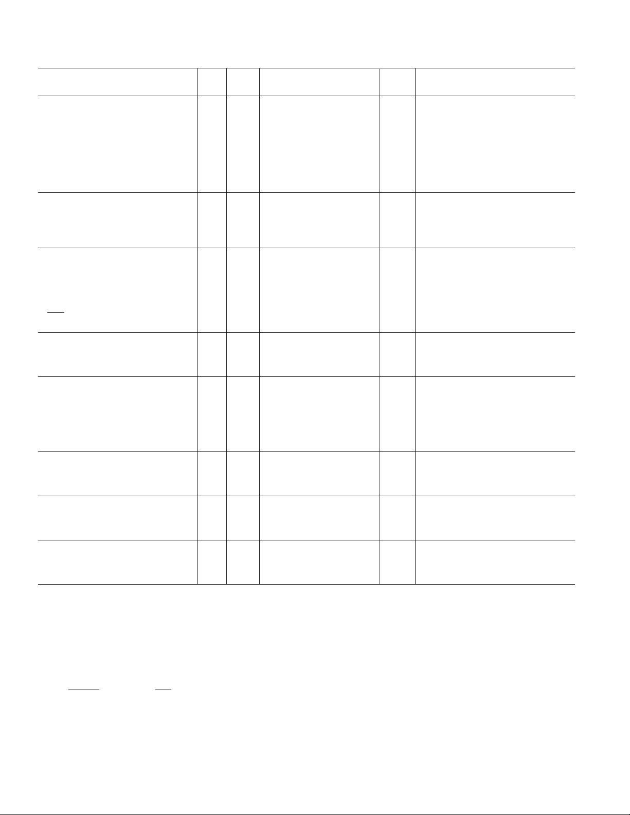
+V
SENSE
1mA
IN
S
1mA
TTL
INPUT
+V
S
EXPLANATION OF TEST LEVELS
Test Level
I – 100% production tested.
II – 100% production tested at +25°C, and sample tested at
specified temperatures.
III – Sample tested only.
IV – Parameter is guaranteed by design and characterization
testing.
V – Parameter is a typical value only.
VI – All devices are 100% production tested at +25°C; 100%
production tested at temperature extremes for military
devices; sample tested at temperature extremes for
commercial/industrial devices.
+V
S
V
BANDGAP
100Ω
V
REF
450Ω
50Ω 50Ω
OUTPUT
HOLD
T/H
1250Ω
Equivalent Circuits
CAUTION
ESD (electrostatic discharge) sensitive device. Electrostatic charges as high as 4000 V readily
accumulate on the human body and test equipment and can discharge without detection.
Although the AD9661A features proprietary ESD protection circuitry, permanent damage may
occur on devices subjected to high energy electrostatic discharges. Therefore, proper ESD
precautions are recommended to avoid performance degradation or loss of functionality.
WARNING!
ESD SENSITIVE DEVICE
REV. 0
–3–
AD9661A
Pin Function
PIN DESCRIPTIONS
OUTPUT Analog laser diode current output. Connect to cathode of laser diode, anode connected to +V
to V
POWER LEVEL Analog voltage input, V
during calibration as follows:
REF
+ 1.6 V. Output current is set proportional to the POWER LEVEL
REF
I
MONITOR
V
POWER LEVEL
=
R
GAIN
–V
+ 50 Ω
REF
externally.
S
CAL TTL/CMOS compatible, feedback loop T/H control signal. Logic LOW enables calibration mode, and
the feedback loop T/H goes into track mode 13 ns after (the aperture delay) PULSE goes logic HIGH
(there is no aperture delay if PULSE goes high before CAL transitions to a LOW level). Logic HIGH disables the T/H and immediately places it in hold mode. PULSE should be held HIGH while calibrating.
Floats logic HIGH.
HOLD External hold capacitor for the bias loop T/H. Approximate droop in the output current while CAL is
logic HIGH is:
±∆I
OUT
18 ×10
=
Bandwidth of the loop is:
BW ≈
PULSE TTL/CMOS compatible, current control signal. Logic HIGH supplies I
LOW turns I
PULSE 2 TTL/CMOS compatible, current control signal. Logic LOW supplies I
HIGH turns I
SENSE IN Analog current input, I
anode of the PIN diode, with the PIN cathode connected to +V
off. Floats logic HIGH.
OUT
off. Floats logic HIGH.
OUT
MONITOR
–9
t
HOLD
C
HOLD
1
2 π(550 Ω)C
, from PIN photo detector diode. SENSE IN should be connected to the
HOLD
to the laser diode. Logic
OUT
to the laser diode. Logic
OUT
or another positive voltage. Voltage at
S
SENSE IN varies slightly with temperature and current, but is typically 1.0 V.
GAIN External connection for the feedback network of the transimpedance amplifier. External feedback network,
R
GAIN
and C
, should be connected between GAIN and POWER MONITOR. See text for choosing
GAIN
values.
POWER MONITOR Output voltage monitor of the internal feedback loop. Voltage is proportional to feedback current from
photo diode, I
MONITOR
.
DISABLE TTL/CMOS compatible, current output disable circuit. Logic LOW for normal operation; logic HIGH
disables the current outputs to the laser diode, and drives the voltage on the hold capacitors close to V
REF
(minimizes the output current when the device is re-enabled). DISABLE floats logic HIGH.
V
+V
REF
S
Analog Voltage output, internal bandgap voltage reference, ~1.8 V, provided to user for power level offset.
Power Supply, nominally +5 V. All +VS connections should be tied together externally.
GROUND Ground reference. All GROUND connections should be tied together externally.
LEVEL SHIFT IN Analog input to the on board level shift circuit. Input Range 0.1 V – 1.6 V.
LEVEL SHIFT OUT Voltage output from on board level shift circuit. Connect to POWER LEVEL externally to use the on
board level shift circuit. Output voltage is V
LEVEL SHIFT OUT
= V
LEVEL SHIFT IN
+V
REF
.
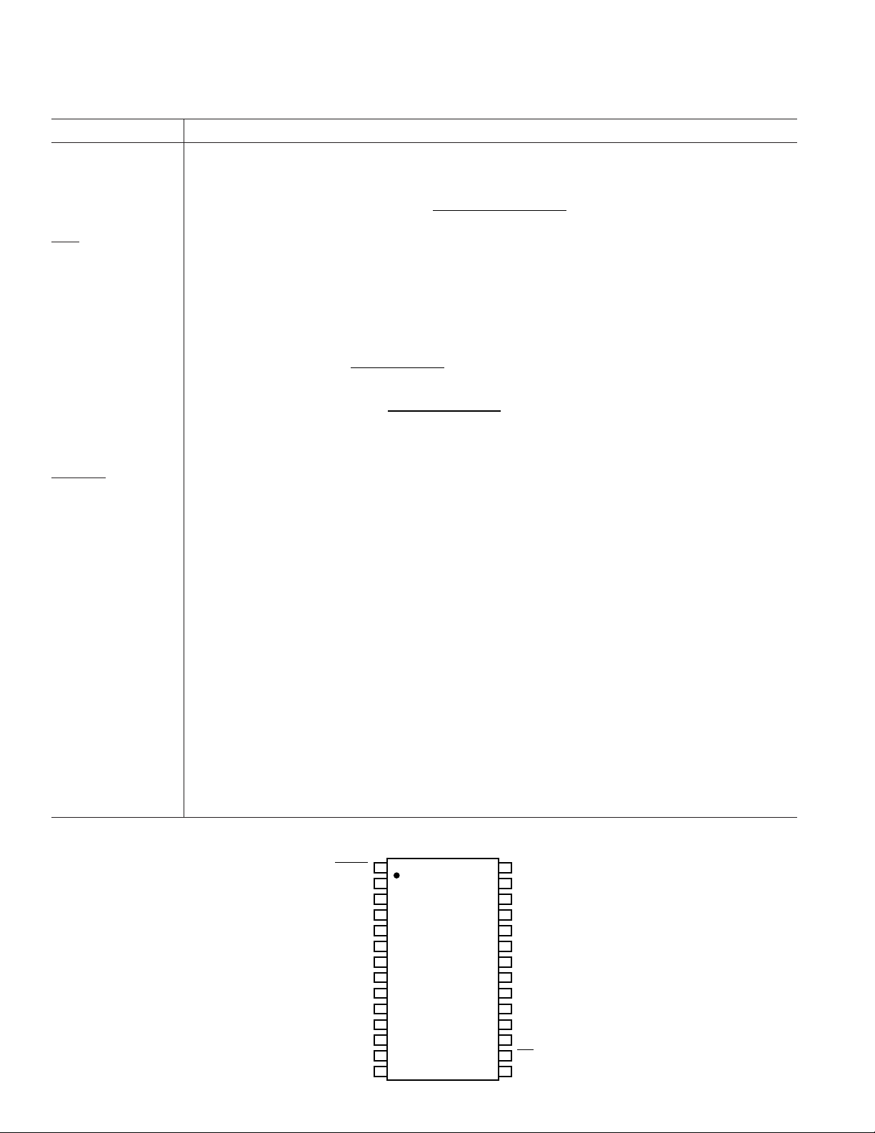
PIN ASSIGNMENTS
PULSE2
DNC
V
REF
LEVEL SHIFT IN
GAIN
POWER MONITOR
SENSE INPUT
GROUND
+V
GROUND
HOLD
POWER LEVEL
LEVEL SHIFT OUT
DISABLE
1
2
3
4
5
6
AD9661AKR
7
(Not to Scale)
8
9
S
10
11
12
13
14
–4–
28
27
26
25
24
23
22
21
20
19
18
17
16
15
+V
S
GROUND
OUTPUT
GROUND
OUTPUT
GROUND
OUTPUT
GROUND
OUTPUT
GROUND
+V
S
GROUND
CAL
PULSE1
REV. 0

AD9661A
THEORY OF OPERATION
The AD9661A combines a very fast output current switch with
an onboard analog light power control loop to provide the user
with a complete laser diode driver solution. The block diagram
illustrates the key internal functions. The control loop of the
AD9661A adjusts the output current level, I
photo diode feedback current, I
MONITOR
, into SENSE IN is pro-
, so that the
OUT
portional to the analog input voltage at POWER LEVEL. Since
the monitor current is proportional to the laser diode light
power, the loop effectively controls laser power to a level proportional to the analog input. The control loop should be periodically calibrated (see Choosing C
The disable circuit turns off I
OUT
).
HOLD
and returns the hold capacitor
voltages to their minimum levels (minimum output current)
when DISABLE = logic HIGH. It is used during initial power
up of the AD9661A or during time periods where the laser is
inactive. When the AD9661A is re-enabled the control loop
must be recalibrated.
Normal operation of the AD9661A involves the following (in
order, see Figure 1):
1. The AD9661A is enabled (DISABLE = logic LOW).
2. The input voltage (POWER LEVEL) is driven to the
appropriate level to set the calibrated laser diode output
power level.
3. The feedback loop is closed for calibration (
LOW, and PULSE = logic HIGH), and then opened (
CAL = logic
CAL
= logic HIGH).
4. While the feedback loop is open, the laser is pulsed on and
off by PULSE.
5. The feedback loop is periodically recalibrated as needed.
6. The AD9661A is disabled when the laser will not be pulsed
for an indefinite period of time.
Control Loop Transfer Function
The relationship between I
I
MONITOR
MONITOR
=
and V
POWER LEVEL
V
POWER LEVEL–VREF
(R
GAIN
+50 Ω)
is
once the loop is calibrated. When the loop is open (CAL = logic
HIGH), the output current, I
, is proportional to the held
OUT
voltage at HOLD; the external hold capacitor on this pin
determines the droop error in the output current between
calibrations.
The sections below discuss choosing the external components in
the feedback loop for a particular application.
Choosing R
The gain resistor, R
GAIN
, allows the user to match the feedback
GAIN
loop’s transfer function to the laser diode/photo diode
combination.
The user should define the maximum laser diode output power
for the intended application, P
photo diode monitor current, I
diode transfer function is illustrated below. R
, and the corresponding
LD MAX
MONITOR MAX
. A typical laser
GAIN
should be
chosen as:
R
GAIN
4
3
CONSTANT WRITE POWER
2
OPTICAL OUTPUT – mW
1
1.6 V
=
I
MONITOR MAX
–50Ω
0°C CASE
25°C
CASE
50°C CASE
DISABLE
CAL
PULSE
CALIBRATED LEVEL
LASER
OUTPUT POWER
Figure 2. Laser Diode Current-to-Optical Power Curve
POWER-UP
OR LASER
NOT IN USE
CAL
TIME
RECALIBRATE
HOLD TIME
LASER POWER
MODULATED
Figure 1. Normal Operating Mode
0
0 12020 40 60 80 100
FORWARD CURRENT – mA
I
OUT
REV. 0
–5–

AD9661A
The laser diode’s output power will then vary from 0 to P
for an input range of V
REF
to V
+1.6 V @ the POWER
REF
LD MAX
LEVEL input.
Minimum specifications for I
choosing R
. Users are cautioned that laser diode/photo
GAIN
MONITOR MAX
should be used when
diode combinations that produce monitor currents that are less
than I
MONITOR MAX
in the equation above will produce higher laser output power than predicted, which may damage the laser
diode. Such a condition is possible if R
is calculated using
GAIN
typical instead of minimum monitor current specifications. In
that case the input range to the AD9661A POWER LEVEL
input should be limited to avoid damaging laser diodes.
Another approach would be to use a potentiometer for R
This allows users to optimize the value of R
for each laser
GAIN
GAIN
.
diode/photo diode combination’s monitor current. The drawback to this approach is that potentiometers’ stray inductance
and capacitance may cause the transimpedance amplifier to
overshoot and degrade its settling, and the value of C
GAIN
may
not be optimized for the entire potentiometer’s range.
C
optimizes the response of the transimpedance amplifier
GAIN
and should be chosen as from the table below. Choosing C
GAIN
larger than the recommended value will slow the response of the
amplifier. Lower values improve TZA bandwidth but may cause
the amplifier to oscillate.
Table I.
Recommended
R
GAIN
C
GAIN
To choose a value, the user will need to determine the amount
of time the loop will be in hold mode, t
, the maximum
HOLD
change in laser output power the application can tolerate, and
the laser efficiency (defined as the change in laser output power
to the change in laser diode current). As an example, if an application requires 5 mW of laser power ± 5%, and the laser diode
efficiency is 0.25 mW/mA, then
∆I
=5mW ×(5%)/ 0.25
MAX
mW
mA
=1.0 mA
If the same application had a hold time requirement of 250 µs,
then the minimum value of the hold capacitor would be:
–9
C
HOLD
18×10
=
×250 µs
1.0 mA
=4.5 nF
When determining the calibration time, the T/H and the external hold capacitor can be modeled using the simple RC circuit
illustrated below.
AD9661A
POWER LEVEL
POWER MONITOR
T/H
TZA
R
HOLD
EXTERNAL HOLD
C
HOLD
CAPACITOR
2.5 kΩ 2 pF
1.5 kΩ 3 pF
1 kΩ 4 pF
500 Ω 8 pF
Choosing C
Choosing values for the hold capacitor, C
HOLD
, is a tradeoff
HOLD
between output current droop when the control loop is open,
and the time it takes to calibrate and recalibrate the laser power
when the loop is closed.
The amount of output current droop is determined by the value
of the hold capacitor and the leakage current at that node.
When the control loop is open (
CAL logic HIGH), the pin connection for the hold capacitor (HOLD) is a high impedance input. Leakage current will range from ± 200; this low current
minimizes the droop in the output power level. Assuming the
worst case current of ±200 nA, the output current will change
as follows:
±∆I
OUT
18 ×10
=
C
–9
HOLD
Figure 3. Circuitry Model for Determining Calibration Times
Using this model, the voltage at the hold capacitor is
C
V
HOLD
=V
t =0
+(V
–V
t =
t =0
∞
)1–e
–t
τ
where t = 0 is when the calibration begins (CAL goes logic
LOW), V
is the voltage on the hold cap at t = 0, V
t = 0
t = ∞
is the
steady state voltage at the hold cap with the loop closed, and
τ = R
V
C
HOLD
be estimated from the following table and chart:
is the time constant. With this model the error in
C
HOLD
for a finite calibration time, as compared to V
t = ∞
, can
Table II.
t
CALIBRATION
% Final Value Error %
7τ 99.9 0.09
6τ 99.7 0.25
5τ 99.2 0.79
4τ 98.1 1.83
3τ 95.0 4.97
2τ 86.5 13.5
τ 63.2 36.8
–6–
REV. 0
AD9661A
100
90
80
70
60
50
40
30
% FINAL VALUE – % of Volts
20
10
0
051
24
TIME CONSTANTS – t
3
Figure 4. Calibration Time
Initial calibration is required after power-up or any other time
the laser has been disabled. Disabling the AD9661A drives the
hold capacitor to ≈V
. In this case, or in any case where the
REF
output current is more than 10% out of calibration, R will range
from 300 Ω to 550 Ω for the model above; the higher value should
be used for calculating the worst case calibration time. Following
the example above, if C
were chosen as 4.5 nF, then
HOLD
τ = RC = 550 Ω × 4.5 nF would be 2.48 µs. For an initial
calibration error < 1%, the initial calibration time should be
> 5 τ = 12.36 µs.
Initial calibration time will actually be better than this calculation indicates, as a significant portion of the calibration time will
be within 10% of the final value, and the output resistance in
the AD9660’s T/H decreases as the hold voltage approaches its
final value.
Recalibration is functionally identical to initial calibration, but
the loop need only correct for droop. Because droop is assumed
to be a small percentage of the initial calibration (< 10%), the
resistance for the model above will be in the range of 75 Ω to
140 Ω. Again, the higher value should be used to estimate the
worst case time needed for recalibration.
Continuing with the example above, since the droop error during hold time is < 5%, we meet the criteria for recalibration and
τ = RC = 140 Ω × 4.5 nF = 0.64 µs. To get a final error of 1%
after recalibration, the 5% droop must be corrected to within a
20% error (20% × 5% = 1%). A 2 τ recalibration time of 1.2 µs
is sufficient.
Continuous Recalibration
In applications where the hold capacitor is small (< 500 pF) and
the WRITE PULSE signals always have a pulse width > 25 ns,
the user may continuously calibrate the feedback loop. In such
an application, the
CAL signal should be held logic LOW, and
the PULSE signal will control loop calibration via the internal
AND gate. In such application, it is important to optimize the
layout for the TZA (POWER MONITOR, GAIN, R
C
).
GAIN
GAIN
and
Driving the Analog Inputs
The POWER LEVEL input of the AD9661A drives the track
and hold amplifier and allows the user to adjust the amount of
output current as described above. The input voltage range is
V
to V
REF
V
for a ground based signal (see below for description of the
REF
+ 1.6 V, requiring the user to create an offset of
REF
on board level shift circuit). The circuit below will perform the
level shift and scale the output of a DAC whose output is from
ground to a positive voltage. This solution is especially attractive because both the DAC and the op amp can run off a single
+5 V supply, and the op amp doesn’t have to swing rail to rail.
R2
V
= V
+
DAC
R1
R2
+5V
OP191
POWER LEVEL
AD9661A
BIAS LEVEL
V
REF
DAC
V
REF
V
DAC
R1
R1
R2
Figure 5. Driving the Analog Inputs
Using the Level Shift Circuit
The AD9661A includes an on board level shift circuit to provide
the offset described above. The input, LEVEL SHIFT IN, has
an input range from 0.1 V to 1.6 V. The output, LEVEL
SHIFT OUT, has a range from V
REF
to V
+1.6 V, and can
REF
drive POWER MONITOR. The linearity of the level shift circuit is poor for inputs below 100 mV. Between 100 mV and
1.6 V it is about 7 bits accurate.
Layout Considerations
As in all high speed applications, proper layout is critical; it is
particularly important when both analog and digital signals are
involved. Analog signal paths should be kept as short as
possible, and isolated from digital signals to avoid coupling in
noise. In particular, digital lines should be isolated from
OUTPUT, SENSE IN, POWER LEVEL, LEVEL SHIFT IN
POWER MONITOR, and HOLD traces. Digital signal paths
should also be kept short, and run lengths matched to avoid
propagation delay mismatch.
Layout of the ground and power supply circuits is also critical.
A single, low impedance ground plane will reduce noise on the
circuit ground. Power supplies should be capacitively coupled
to the ground plane to reduce noise in the circuit. 0.1 µF
surface mount capacitors, placed as close as possible to the
AD9661A +V
connections, and the +VS connection to the laser
S
diode meet this requirement. Multilayer circuit boards allow
designers to lay out signal traces without interrupting the ground
plane, and provide low impedance power planes to further
reduce noise.
REV. 0
–7–

AD9661A
Minimizing the Impedance of the Output Current Path
Because of the very high current slew that the AD9661A is
capable of producing (120+ mA in 1.5 ns), the inductance of
the output current path to and from the laser diode is critical.
A good layout of the output current path will yield high quality
light pulses with rise times of about 1.5 ns and less than 5%
overshoot. A poor layout can result in significant overshoot and
ringing. The most important guideline for the layout is to minimize the impedance (mostly inductance) of the output current
path to the laser.
It is important to recognize that the laser current path is a
closed loop. The figure illustrates the path that current travels:
(1) from the +V
connection at the anode of the laser to the
S
cathode (2) from the cathode to the output pins of the
AD9661A (3) through the output drive circuit of the
AD9661A, (4) through the return path (GROUND plane in the
illustration) (5) through the bypass capacitors back to the +V
S
connection of the laser diode. The inductance of this loop can
be minimized by placing the laser as close to the AD9661A as
possible to keep the loop short, and by placing the send and return paths on adjacent layers of the PC board to take advantage
of mutual coupling of the path inductances. This mutual coupling effect is the most important factor in reducing inductance
in the current path.
The trace from the output pins of the AD9661A to the cathode
of the laser should be several millimeters wide and should be as
direct as possible. The return current will choose the path of
least resistance. If the return path is the GROUND plane, it
should have an unbroken path, under the output trace, from the
laser anode back to a the AD9661A. If the return path is not
the ground plane (such as on a two layer board, or on the +V
S
plane), it should still be on the board plane adjacent to the
plane of the output trace. If the current cannot return along a
path that follows the output trace, the inductance will be drastically increased and performance will be degraded.
OUTPUT PIN
CONNECTIONS
26
25
AD9661A
24
23
22
Optimizing the Feedback Layout
In applications where the dynamic performance of the analog
feedback loop is important, it is necessary to optimize the layout
of the gain resistor, R
, as well as the monitor current path to
GAIN
SENSE IN. Such applications include systems which recalibrate the write loop on pulses as short as 25 ns, and closed-loop
applications.
The best possible TZA settling will be achieved by using a single
carbon surface mount resistor (usually 5% tolerance) for R
and small surface mount capacitor for C
. Because the
GAIN
GAIN
GAIN pin (Pin 5) is essentially connected to the inverting input
of the TZA, it is very sensitive to stray capacitance. R
GAIN
should be placed between Pin 5 and Pin 6, as close as possible
to Pin 5. Small traces should be used, and the ground and +V
S
planes adjacent to the trace should be removed to further minimize stray capacitance.
The trace from SENSE IN to the anode of the PIN photodetector should be thin and routed away from the laser cathode trace.
Example Calculations
The example below (in addition to the one included in the sections above) should guide users in choosing R
GAIN
, C
GAIN
, the
hold capacitor values, and worst case calibration times.
System Requirements:
• Laser power: 4 mW ± 2%
• Hold Time: 0.5 ms
Laser diode/photo diode characteristics:
• Laser efficiency 0.3 mW/mA
• Monitor current : 0.2 mA/mW
• From the laser power requirements and efficiency we can
estimate:
∆I
OUT MAX
PIN ASSIGNMENTS
2
1
+VS PLANE
= 4 mW ×(2.0%)/ 0.3
BYPASS CAPS
MUTUAL COUPLING
REDUCES INDUCTANCE
mW
mA
= 266.6 µA.
5
3
GROUND PIN
CONNECTIONS
21
20
19
LASER DIODE CURRENT
PATH SEGMENTS (See Text)
Figure 6. Laser Diode Current Loop
–8–
GROUND PLANE
4
REV. 0

AD9661A
• Choosing a hold caps based on this:
–9
C
HOLD
18×10
=
×0.5ms
266.6µA
=0.034µF
• The initial calibration time for < 0.1% error:
7 τ=7×RC = 7× 550 Ω×0.034 µF =130.9 µs
• Recalibration for a 0.1% error after 2% droop (need to
correct within 5%):
3 τ = 3 RC = 3 × 140 Ω × 0.034 µF = 14.28 µs
Typical Performance Characteristics
PULSE INPUT (TTL)
• From the monitor current specification and the max power
specified:
I
MONITOR MAX
= 4 mW
0.2 mA
mW
= 800 µA
and
1.6 V
=
I
MONITOR MAX
–50Ω=2.0 kΩ
•C
GAIN
R
GAIN
would be chosen from the table as 3 pF for safe
compensation.
LASER POWER
20mV/DIV
LASER POWER
20mV/DIV
20ns/DIV
REV. 0
1ns/DIV
Figure 7. Driving 78N20 Laser Diode @ 5 mW
–9–

AD9661A–Typical Performance Characteristics
180
160
140
120
100
– mA
OUT
I
80
60
40
20
0
1.7 3.22
2.3 2.9
2.6
V
HOLD
3.5 3.8 4.1 4.4
– V
4.2
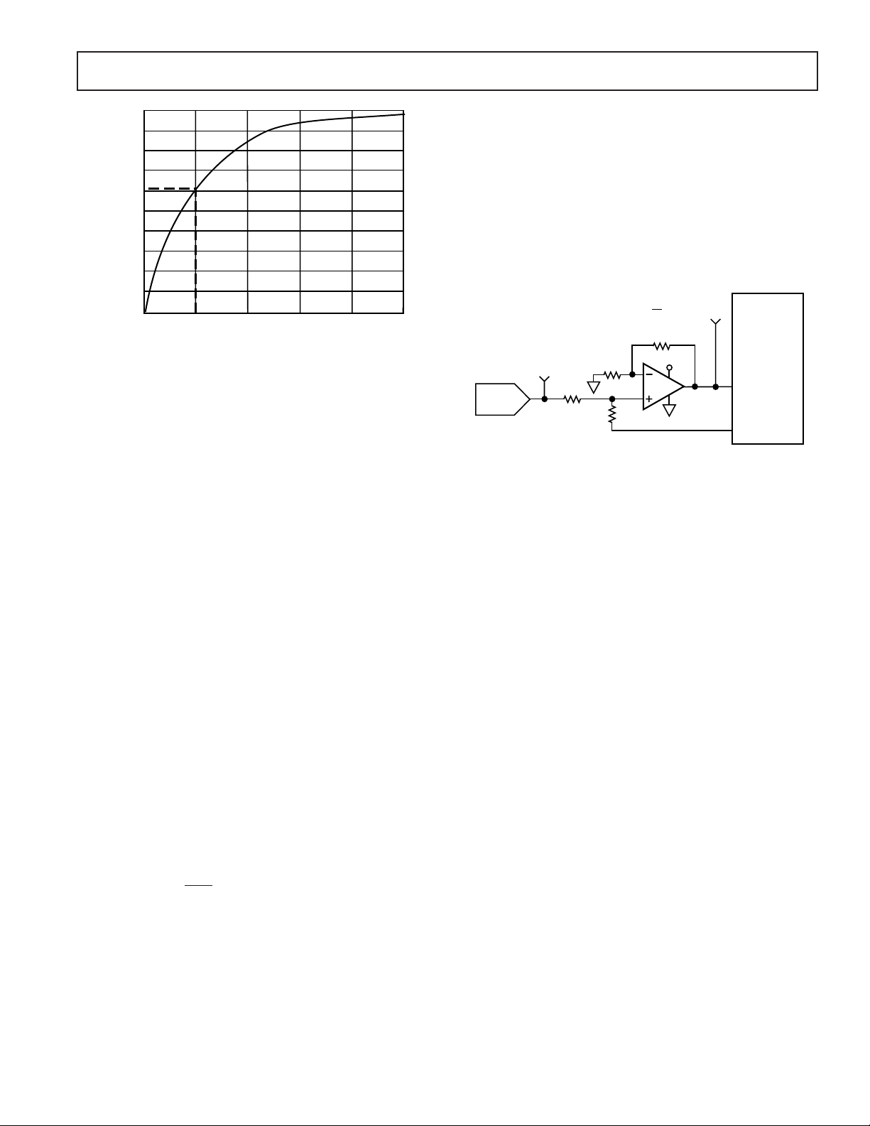
Figure 8. Typical AD9661A V/I Transfer Function
10mV
AD9661A
POWER MONITOR
1kΩ
2pF
3V
2V
LOW
HIGH
GAIN
POWER LEVEL
PULSEL
SENSE IN
OUTPUT
HOLD
20ns
+5V
1kΩ 10Ω
33pF
MPSH81
TO
SCOPE
Figure 9. Typical AD9661A Closed-Loop Pulse Response
–10–
REV. 0

AD9661A
AD9661A EVALUATION BOARD
The AD9661A Evaluation Board is comprised of two printed
circuit boards. The Laser Diode Driver (LDD) Resource Board
is both a digital pattern generator and an analog reference generator (see LDD Resource Board Block Diagram.) The board is
controlled by an IBM compatible personal computer through a
standard printer cable. The resource board interfaces to the
AD9661A DUT board, which contains the AD9661A, a level
shift circuit for the analog input, and a socket for an N type
STANDARD PARALLEL
PRINTER CABLE
IBM-COMPATIBLE
PC
WITH WINDOWS
PARALLEL
PRINTER PORT
40MHz
CLOCK
OSCILLATOR
P1
CENTRONICS
CONNECTOR
LASER DIODE DRIVER RESOURCE BOARD
READBACK
LATCH
DIGITAL PATTERN GENERATOR
8
DAC 1
8
DAC 2
ANALOG REFERENCE
32K x 16
MEMORY
ADDRESS
COUNTER
AND
RESOURCE
CONTROLLER
0–2.55V
X1
0–2.55V
X1
laser diode. A dummy load circuit for the laser diode is included for evaluation. Power for all the boards is provided
through the banana jacks on the AD9661A DUT board.
These should be connected to a linear, +5 V power supply.
Schematics for the LDD Resource Board, AD9661A DUT,
and Dummy Load are included, along with a bill of material and layout information. Please contact Applications for
additional information.
OUTPUT
SMB
CONNECTORS
PULSE
WIDTH
MODULATOR
(AD9560)
OUTPUT
BUFFER
J4
J5
J7
J8
J6
J2
J3
20-PIN
HEADER
12
11
PULSE1 (JPUL)
CAL (JCALB)
DISABLE (JDIS)
(JPULB)
PULSE2
UNUSED
TRIGGER
EXTERNAL LEVEL SHIFT CIRCUIT
R9
17–20
1–10
INTERFACE TO
AD9661A
EVALUATION
BOARD
AD9661A
LEVEL SHIFT IN
R8
+5V POWER SUPPLY
GROUND
Figure 10. LDD Resource Board Block Diagram
INPUT SMB CONNECTORS
FOR DIGITAL CONTROLS
5
20
20-PIN HEADER
FOR ANALOG
CONTROLS
OPTIONAL
LEVEL SHIFT
CIRCUIT
AD9661A
DUMMY LOAD CIRCUIT/
LASER DIODE SOCKET
AD9661A
EVALUATION BOARD
Figure 11. Evaluation Board Block Diagram
REV. 0
–11–

AD9661A
OUTLINE DIMENSIONS
Dimensions shown in inches and (mm).
28-Pin Plastic SOIC
(R-28)
0.712 (18.08)
0.700 (17.78)
28 15
0.300 (7.60)
0.292 (7.40)
0.012 (0.30)
0.004 (0.10)
PIN 1
0.0500
(1.27)
BSC
0.019 (0.48)
0.014 (0.36)
0.419 (10.64)
0.393 (9.98)
141
SEATING
PLANE
0.104 (2.64)
0.093 (2.36)
0.013 (0.33)
0.009 (0.23)
C2079–6–10/95PRINTED IN U.S.A.
0.04 (1.02)
0.024 (0.61)
–12–
REV. 0
 Loading...