A
D
F
E
e
o
o
6
-
D
n
6
a
f
Sof
e
a
C
A
u
u
o
i
L
e
o
C
g
t
B
t
t
(
a
o
D
G
a
S
w
l
o
l
U
,
r
e
e
C
D
u
g
A
L
Z
u
C
u
r
e
9642
Quick
nalog-
Start
o-Digit
uide fo
l Conv
testin
rter (
the
DC) C
stome
Eval
ation
oard U
B
ard H
sing th
C-AD
FPGA
-EVA
based
CZ
aptur
quipm
► Anal
► Anal
► PC
► USB
► AD9
► HSC
ocume
► AD9
► Visu
► High
► Inter
twar
► Visu
► SPI
igure 1: AD
nt Needed
g signal so
g Clock S
2.0 port rec
42 evaluat
ADC-EVA
ts Needed
42 Datash
lAnalog C
Speed AD
acing to Hi
Needed
lAnalog
ontroller
9642 Evalua
rce and an
urce
ommended
on board
CZ FPGA
et
nverter Ev
SPI Contr
h Speed A
ion Board
i-aliasing fi
USB 1.1-c
Based Data
luation Too
l Software
Cs via SPI
ith HSC-A
ter
mpatible)
Capture Bo
User Man
ser Manua
AN-877
C_EVALC
ard
al, AN-905
l, AN-878
Data Capt
re Board
1

All documents and software are available at http://www.analog.com/fifo.
For any questions please send an email to highspeed.converters@analog.com.
Testing
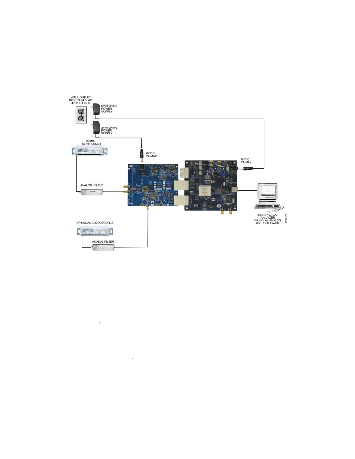
1. Connect the AD9642 evaluation board and the HSC-ADC-EVALCZ board together as
shown in Figure 1.
2. Connect one 6V, 2A switching power supply (such as the CUI EPS060250UH-PHP-SZ
supplied) to the AD9642 board.
3. Make sure a jumper is installed on header J9 at the 2.5V position on the HSC-ADC-
EVALCZ evaluation board to set the FPGA I/O voltage to 2.5V. Connect one 6V, 2A
switching power supply (such as the CUI EPS060250UH-PHP-SZ supplied) to the HSCADC-EVALCZ board.
4. Connect the HSC-ADC-EVALCZ board to the PC with a USB cable. (Connect to J6.)
5. On the ADC evaluation board, make sure that jumpers are installed on headers P105, P108,
P107, P110, and P104 for the default setup.
6. On the ADC evaluation board, provide a clean, low jitter clock source to connector J506 at
the desired ADC conversion rate. If the AD9642 input clock divider is used provide a clock
into connector J506 at the appropriate rate which will be divided to your desired clock rate.
The input clock level should be between 10dBm and 14dBm.
7. On the ADC evaluation board, use a clean signal generator with low phase noise to provide
an input signal to the analog input at connector J301 (Channel A). Use a 1 m, shielded,
RG-58, 50 Ω coaxial cable to connect the signal generator. For best results use a narrow-
band, band-pass filter with 50 Ω terminations and an appropriate center frequency. (ADI uses
TTE, Allen Avionics, and K&L band-pass filters.) In order for the input level to be near the
ADC’s full scale, the generator level should be set to 8dBm to 12dBm – this level depends on
the input frequency and any losses in bandpass filters.
8. Open VisualAnalog on the PC. “AD9642” should be listed in the status bar of the “New
Canvas” window. Select the template that corresponds to the type of testing that you are
performing. Select ‘Yes’ when VisualAnalog prompts for programming the FPGA. The
‘DONE’ LED should illuminate on the HSC-ADC-EVALCZ board indicating that the FPGA
has been correctly programmed. (If Visual Analog does not prompt for programming the
FPGA select the ADC Data Capture Settings window and click on the ‘Capture Board’ tab.
In the FPGA box select program to configure the FPGA. If using parts that are branded
“XCPZ” with a date code other than 1126, select the AD9642_0.bin file to program the
FPGA.)
9. Next open the SPI Controller software. If prompted for a configuration file, select the
configuration file titled AD9642_14Bit_250MSspiR03.cfg. If not, check the title bar of the
window to see which configuration is loaded. If necessary, choose “Cfg Open” from the
“File” menu and select one of the configuration files named above. Note that the CHIP ID(1)
field may be filled whether the correct SPI Controller configuration file is loaded or not.
2
 Loading...