Quad, 12-Bit, 170 MSPS/210 MSPS
A
T
FEATURES
4 ADCs in one package
JESD204 coded serial digital outputs
On-chip temperature sensor
−95 dB channel-to-channel crosstalk
SNR: 65 dBFS with AIN = 85 MHz at 210 MSPS
SFDR: 77 dBc with AIN = 85 MHz at 210 MSPS
Excellent linearity
DNL: ±0.28 LSB (typical)
INL: ±0.7 LSB (typical)
780 MHz full power analog bandwidth
Power dissipation: 325 mW per channel at 210 MSPS
1.25 V p-p input voltage range, adjustable up to 1.5 V p-p
1.8 V supply operation
Clock duty cycle stabilizer
Serial port interface features
Power-down modes
Digital test pattern enable
Programmable header
Programmable pin functions (PGMx, PDWN)
Serial Output 1.8 V ADC
AD9639
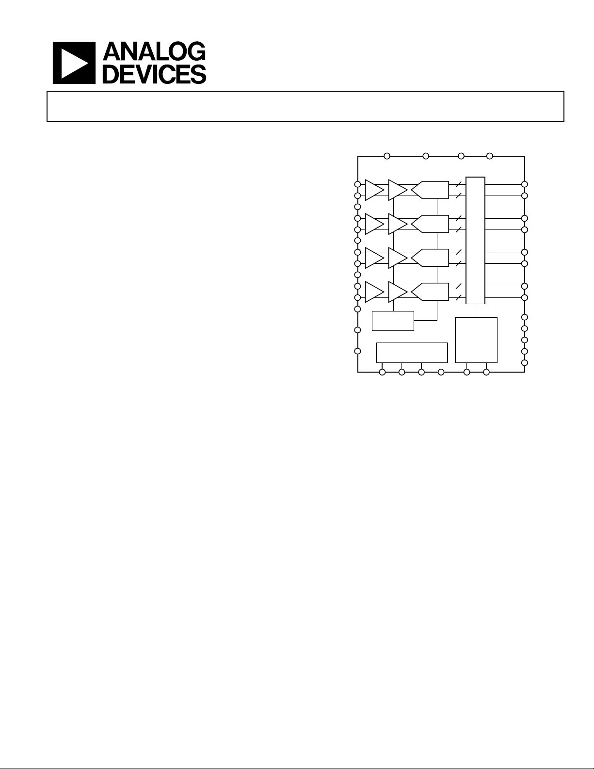
FUNCTIONAL BLOCK DIAGRAM
VDD PDWN DRVDD DRGND
AD9639
VIN + A DOUT + A
VIN – A
VCM A
VIN + B
VIN – B
VCM B
VIN + C DOUT + C
VIN – C
VCM C
VIN + D
VIN – D
VCM D
RBIAS
EMPOUT
BUF
BUF
BUF
BUF
REFERENCE
SHA
SHA
SHA
SHA
SERIAL
PORT
PIPELINE
ADC
PIPELINE
ADC
PIPELINE
ADC
PIPELINE
ADC
12
12
12
DATA SERIALI ZER, ENCODER, AND
12
DATA RATE
MULTIPLIER
CHANNEL A
CHANNEL B
CHANNEL C
CML DRIVERS
CHANNEL D
DOUT – A
DOUT + B
DOUT – B
DOUT – C
DOUT + D
DOUT – D
PGM3
PGM2
PGM1
PGM0
RESET
APPLICATIONS
Communication receivers
Cable head end equipment/M-CMTS
Broadband radios
Wireless infrastructure transceivers
Radar/military-aerospace subsystems
Test equipment
GENERAL DESCRIPTION
The AD9639 is a quad, 12-bit, 210 MSPS analog-to-digital converter (ADC) with an on-chip temperature sensor and a high
speed serial interface. It is designed to support the digitizing
of high frequency, wide dynamic range signals with an input
bandwidth of up to 780 MHz. The output data is serialized
and presented in packet format, consisting of channel-specific
information, coded samples, and error code correction.
The ADC requires a single 1.8 V power supply. The input clock
can be driven differentially with a sine wave, LVPECL, CMOS,
or LVDS. A clock duty cycle stabilizer allows high performance
at full speed with a wide range of clock duty cycles. The on-chip
reference eliminates the need for external decoupling and can
be adjusted by means of SPI control.
Various power-down and standby modes are supported. The
ADC typically consumes 150 mW per channel with the digital
link still in operation when standby operation is enabled.
SCLK SDI/
SDIO
SDO CSB
CLK+ CLK–
Figure 1.
Fabricated on an advanced CMOS process, the AD9639 is available in a Pb-free/RoHS-compliant, 72-lead LFCSP package. It is
specified over the industrial temperature range of −40°C to +85°C.
PRODUCT HIGHLIGHTS
1. Four ADCs are contained in a small, space-saving package.
2. An on-chip PLL allows users to provide a single ADC
sampling clock; the PLL distributes and multiplies up to
produce the corresponding data rate clock.
3. The JESD204 coded data rate supports up to 4.2 Gbps
per channel.
4. The AD9639 operates from a single 1.8 V power supply.
5. Flexible synchronization schemes and programmable
mode pins are available.
6. An on-chip temperature sensor is included.
7973-001
Rev. A
Information furnished by Analog Devices is believed to be accurate and reliable. However, no
responsibility is assumed by Analog Devices for its use, nor for any infringements of patents or other
rights of third parties that may result from its use. Specifications subject to change without notice. No
license is granted by implication or otherwise under any patent or patent rights of Analog Devices.
Trademarks and registered trademarks are the property of their respective owners.
One Technology Way, P.O. Box 9106, Norwood, MA 02062-9106, U.S.A.
Tel: 781.329.4700 www.analog.com
Fax: 781.461.3113 ©2009–2010 Analog Devices, Inc. All rights reserved.

AD9639
TABLE OF CONTENTS
Features .............................................................................................. 1
Applications ....................................................................................... 1
Functional Block Diagram .............................................................. 1
General Description ......................................................................... 1
Product Highlights ........................................................................... 1
Revision History ............................................................................... 2
Specifications ..................................................................................... 3
AC Specifications .......................................................................... 4
Digital Specifications ................................................................... 5
Switching Specifications .............................................................. 6
Timing Diagram ........................................................................... 7
Absolute Maximum Ratings ............................................................ 8
Thermal Resistance ...................................................................... 8
ESD Caution .................................................................................. 8
Pin Configuration and Function Descriptions ............................. 9
Typical Performance Characteristics ........................................... 11
Equivalent Circuits ......................................................................... 15
Theory of Operation ...................................................................... 17
Analog Input Considerations ................................................... 17
Clock Input Considerations ...................................................... 19
Digital Outputs ........................................................................... 21
Serial Port Interface (SPI) .............................................................. 29
Hardware Interface ..................................................................... 29
Memory Map .................................................................................. 31
Reading the Memory Map Table .............................................. 31
Reserved Locations .................................................................... 31
Default Values ............................................................................. 31
Logic Levels ................................................................................. 31
Applications Information .............................................................. 35
Power and Ground Recommendations ................................... 35
Exposed Paddle Thermal Heat Slug Recommendations ...... 35
Outline Dimensions ....................................................................... 36
Ordering Guide .......................................................................... 36
REVISION HISTORY
2/10—Rev. 0 to Rev. A
Changes to Differential Input Voltage Range Parameter,
Table 1 ................................................................................................ 3
Changes to Table 7 ............................................................................ 9
Changes to Digital Outputs and Timing Section ....................... 25
Change to Addr. (Hex) 0x01, Table 15 ......................................... 32
5/09—Revision 0: Initial Version
Rev. A | Page 2 of 36

AD9639
SPECIFICATIONS
AVDD = 1.8 V, DRVDD = 1.8 V, T
otherwise noted.
Table 1.
AD9639BCPZ-170 AD9639BCPZ-210
Parameter1 Temp Min Typ Max Min Typ Max Unit
RESOLUTION 12 12 Bits
ACCURACY
No Missing Codes Full Guaranteed Guaranteed
Offset Error 25°C −2 ±12 −2 ±12 mV
Offset Matching 25°C 4 12 4 12 mV
Gain Error 25°C −2.8 +1 +4.7 −2.8 +1 +4.7 % FS
Gain Matching 25°C 0.9 2.7 0.9 2.7 % FS
Differential Nonlinearity (DNL) Full ±0.28 ±0.6 ±0.28 ±0.6 LSB
Integral Nonlinearity (INL) Full ±0.45 ±0.9 ±0.7 ±1.3 LSB
ANALOG INPUTS
Differential Input Voltage Range2 Full 1.0 1.25 1.5 1.0 1.25 1.5 V p-p
Common-Mode Voltage Full 1.4 1.4 V
Input Capacitance 25°C 2 2 pF
Input Resistance Full 4.3 4.3 kΩ
Analog Bandwidth, Full Power Full 780 780 MHz
Voltage Common Mode (VCM x Pins)
Voltage Output Full 1.4 1.44 1.5 1.4 1.44 1.5 V
Current Drive Full 1 1 mA
TEMPERATURE SENSOR OUTPUT −1.12 −1.12 mV/°C
Voltage Output Full 739 737 mV
Current Drive Full 10 10 µA
POWER SUPPLY
AVDD Full 1.7 1.8 1.9 1.7 1.8 1.9 V
DRVDD Full 1.7 1.8 1.9 1.7 1.8 1.9 V
I
Full 535 570 610 650 mA
AVDD
I
Full 98 105 111 120 mA
DRVDD
Total Power Dissipation
(Including Output Drivers)
Power-Down Dissipation Full 3 3 mW
Standby Dissipation2 Full 152 173 mW
CROSSTALK Full −95 −95 dB
Overrange Condition3 Full −90 −90 dB
1
See the AN-835 Application Note, Understanding High Speed ADC Testing and Evaluation, for definitions and details on how these tests were completed.
2
AVDD/DRVDD, with link established.
3
Overrange condition is specified as 6 dB above the full-scale input range.
= −40°C, T
MIN
= +85°C, 1.25 V p-p differential input, AIN = −1.0 dBFS, DCS enabled, unless
MAX
Full 1.139 1.215 1.298 1.386 W
Rev. A | Page 3 of 36

AD9639
AC SPECIFICATIONS
AVDD = 1.8 V, DRVDD = 1.8 V, T
otherwise noted.
Table 2.
AD9639BCPZ-170 AD9639BCPZ-210
Parameter1 Temp Min Typ Max Min Typ Max Unit
SIGNAL-TO-NOISE RATIO (SNR)
fIN = 84.3 MHz Full 63.5 64.5 63.2 64.2 dB
fIN = 240.3 MHz 25°C 64.1 63.2 dB
SIGNAL-TO-(NOISE + DISTORTION) (SINAD) RATIO
fIN = 84.3 MHz Full 63.3 64.4 62.8 63.9 dB
fIN = 240.3 MHz 25°C 63.9 63 dB
EFFECTIVE NUMBER OF BITS (ENOB)
fIN = 84.3 MHz Full 10.2 10.4 10.1 10.3 Bits
fIN = 240.3 MHz 25°C 10.3 10.2 Bits
WORST HARMONIC (SECOND)
fIN = 84.3 MHz Full 87.5 78.6 86 77 dBc
fIN = 240.3 MHz 25°C 82 80 dBc
WORST HARMONIC (THIRD)
fIN = 84.3 MHz Full 79 74 76 72.6 dBc
fIN = 240.3 MHz 25°C 84 77 dBc
WORST OTHER (EXCLUDING SECOND OR THIRD)
fIN = 84.3 MHz Full 96 86 90 83.7 dBc
fIN = 240.3 MHz 25°C 88 88 dBc
TWO-TONE INTERMODULATION DISTORTION (IMD)
f
= 140.2 MHz, f
IN1
= 141.3 MHz,
IN2
AIN1 and AIN2 = −7.0 dBFS
f
= 170.2 MHz, f
IN1
= 171.3 MHz,
IN2
AIN1 and AIN2 = −7.0 dBFS
1
See the AN-835 Application Note, Understanding High Speed ADC Testing and Evaluation, for definitions and details on how these tests were completed.
2
Tested at 170 MSPS and 210 MSPS.
MIN
2
= −40°C, T
= +85°C, 1.25 V p-p differential input, AIN = −1.0 dBFS, DCS enabled, unless
MAX
25°C 78 77 dBc
25°C 77 dBc
Rev. A | Page 4 of 36

AD9639
DIGITAL SPECIFICATIONS
AVDD = 1.8 V, DRVDD = 1.8 V, T
otherwise noted.
Table 3.
Parameter1 Temp Min Typ Max Min Typ Max Unit
CLOCK INPUTS (CLK+, CLK−)
Logic Compliance Full LVPECL/LVDS/CMOS LVPECL/LVDS/CMOS
Differential Input Voltage Full 0.2 6 0.2 6 V p-p
Input Voltage Range Full
Internal Common-Mode Bias Full 1.2 1.2 V
Input Common-Mode Voltage Full 1.1 AVDD 1.1 AVDD V
High Level Input Voltage (VIH) Full 1.2 3.6 1.2 3.6 V
Low Level Input Voltage (VIL) Full 0 0.8 0 0.8 V
High Level Input Current (IIH) Full −10 +10 −10 +10 µA
Low Level Input Current (IIL) Full −10 +10 −10 +10 µA
Differential Input Resistance 25°C 16 20 24 16 20 24 kΩ
Input Capacitance 25°C 4 4 pF
LOGIC INPUTS (PDWN, CSB, SDI/SDIO,
SCLK, RESET, PGMx)
2
Logic 1 Voltage Full
Logic 0 Voltage Full
Logic 1 Input Current (CSB) Full 0 0 µA
Logic 0 Input Current (CSB) Full −60 −60 µA
Logic 1 Input Current
(PDWN, SDI/SDIO, SCLK,
RESET, PGMx)
Logic 0 Input Current
(PDWN, SDI/SDIO, SCLK,
RESET, PGMx)
Input Resistance 25°C 30 30 kΩ
Input Capacitance 25°C 4 4 pF
LOGIC OUTPUT (SDO)
Logic 1 Voltage Full 1.2
Logic 0 Voltage Full 0 0.3 0 0.3 V
DIGITAL OUTPUTS (DOUT + x, DOUT − x)
Logic Compliance CML CML
Differential Output Voltage Full 0.8 0.8 V
Common-Mode Voltage Full DRVDD/2 DRVDD/2 V
1
See the AN-835 Application Note, Understanding High Speed ADC Testing and Evaluation, for definitions and details on how these tests were completed.
2
Specified for 13 SDI/SDIO pins on the same SPI bus.
= −40°C, T
MIN
= +85°C, 1.25 V p-p differential input, AIN = −1.0 dBFS, DCS enabled, unless
MAX
AD9639BCPZ-170 AD9639BCPZ-210
AVDD −
0.3
AVDD +
1.6
AVDD −
0.3
AVDD +
1.6
0.8 ×
AVD D
0.2 ×
AVD D
0.8 ×
AVD D
V
0.2 ×
V
AVD D
Full 55 55 µA
Full 0 0 µA
AVDD +
0.3
1.2
AVDD +
0.3
V
Rev. A | Page 5 of 36

AD9639
SWITCHING SPECIFICATIONS
AVDD = 1.8 V, DRVDD = 1.8 V, T
otherwise noted.
Table 4.
Parameter1 Temp Min Typ Max Min Typ Max Unit
CLOCK
Clock Rate Full 100 170 100 210 MSPS
Clock Pulse Width High (tEH) Full 2.65 2.9 2.15 2.4 ns
Clock Pulse Width Low (tEL) Full 2.65 2.9 2.15 2.4 ns
DATA OUTPUT PARAMETERS
Data Output Period or UI
(DOUT + x, DOUT − x)
Data Output Duty Cycle 25°C 50 50 %
Data Valid Time 25°C 0.8 0.8 UI
PLL Lock Time (t
) 25°C 4 4 µs
LOCK
Wake-Up Time (Standby) 25°C 250 250 ns
Wake-Up Time (Power-Down)2 25°C 50 50 s
Pipeline Latency Full 40 40 CLK cycles
Data Rate per Channel (NRZ) 25°C 3.4 4.2 Gbps
Deterministic Jitter 25°C 10 10 ps
Random Jitter 25°C 6 6 ps rms
Channel-to-Channel Bit Skew 25°C 0 0 Seconds
Channel-to-Channel Packet Skew3 25°C ±1 ±1 CLK cycles
Output Rise/Fall Time 25°C 50 50 ps
TERMINATION CHARACTERISTICS
Differential Termination Resistance 25°C 100 100 Ω
APERTURE
Aperture Delay (tA) 25°C 1.2 1.2 ns
Aperture Uncertainty (Jitter) 25°C 0.2 0.2 ps rms
OUT-OF-RANGE RECOVERY TIME 25°C 1 1 CLK cycles
1
See the AN-835 Application Note, Understanding High Speed ADC Testing and Evaluation, for definitions and details on how these tests were completed.
2
Receiver dependent.
3
See the Serial Data Frame section.
= −40°C, T
MIN
= +85°C, 1.25 V p-p differential input, AIN = −1.0 dBFS, DCS enabled, unless
MAX
Full 1/(20 × f
AD9639BCPZ-170 AD9639BCPZ-210
) 1/(20 × f
CLK
) Seconds
CLK
Rev. A | Page 6 of 36
AD9639
L
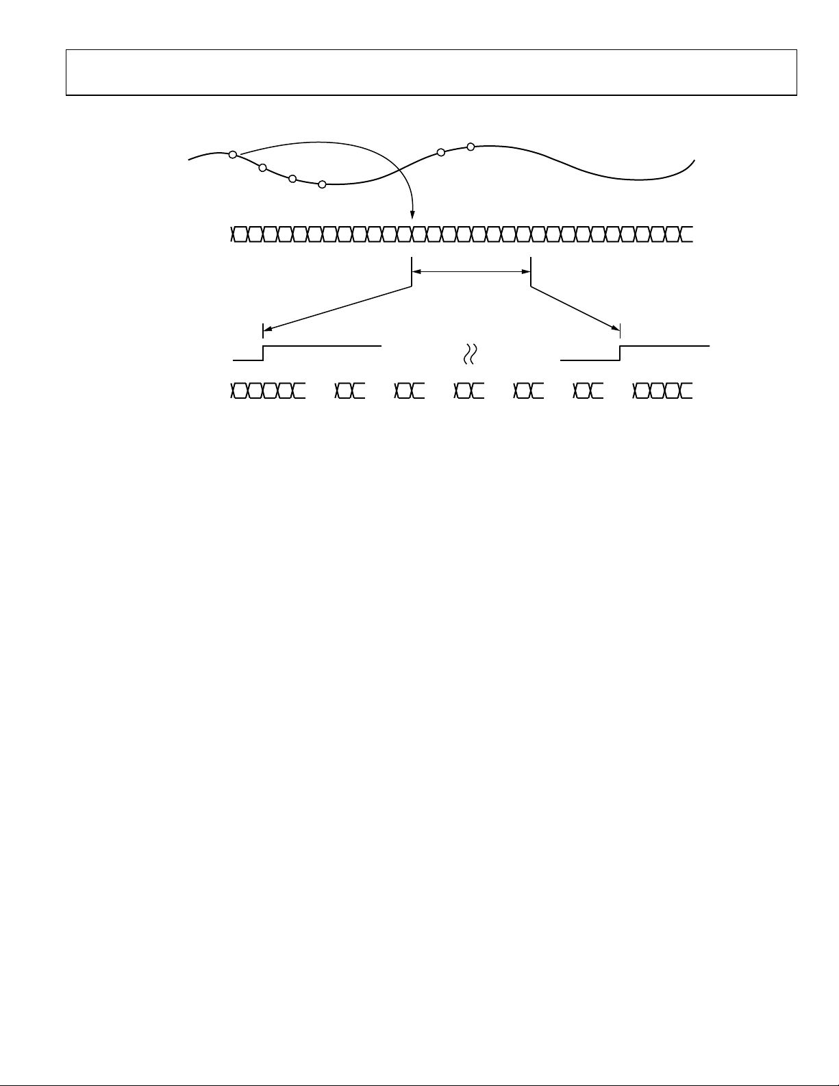
TIMING DIAGRAM
SAMPLE
N + 1
N
ANALOG
INPUT SIGNA
RATE CLOCK
SAMPLE
N – 40
N – 39
N – 38
N – 37
SAMPLE
RATE CLOCK
SERIAL
DATA OUTPUT
SERIAL CO DED SAMPLES : N – 40, N – 39, N – 38, N – 37 ...
... ... ...
...
...
...... ...
07973-002
Figure 2. Timing Diagram
Rev. A | Page 7 of 36
AD9639
ABSOLUTE MAXIMUM RATINGS
Table 5.
Parameter Rating
AVDD to AGND −0.3 V to +2.0 V
DRVDD to DRGND −0.3 V to +2.0 V
AGND to DRGND −0.3 V to +0.3 V
AVDD to DRVDD −2.0 V to +2.0 V
DOUT + x/DOUT − x to DRGND −0.3 V to DRVDD + 0.3 V
SDO, SDI/SDIO, CLK±, VIN ± x, VCM x,
TEMPOUT, RBIAS to AGND
SCLK, CSB, PGMx, RESET, PDWN
to AGND
Storage Temperature Range −65°C to +125°C
Operating Temperature Range −40°C to +85°C
Lead Temperature (Soldering, 10 sec) 300°C
Junction Temperature 150°C
−0.3 V to AVDD + 0.3 V
−0.3 V to AVDD + 0.3 V
Stresses above those listed under Absolute Maximum Ratings
may cause permanent damage to the device. This is a stress
rating only; functional operation of the device at these or any
other conditions above those indicated in the operational
section of this specification is not implied. Exposure to absolute
maximum rating conditions for extended periods may affect
device reliability.
THERMAL RESISTANCE
The exposed paddle must be soldered to the ground plane for the
LFCSP package. Soldering the exposed paddle to the printed
circuit board (PCB) increases the reliability of the solder joints,
maximizing the thermal capability of the package.
Table 6. Thermal Resistance
Package Type θJA θJB θJC Unit
72-Lead LFCSP (CP-72-3) 16.2 7.9 0.6 °C/W
Typical θJA, θJB, and θJC values are specified for a 4-layer board in
still air. Airflow increases heat dissipation, effectively reducing
θ
. In addition, metal in direct contact with the package leads
JA
from metal traces, through holes, ground, and power planes
reduces θ
.
JA
ESD CAUTION
Rev. A | Page 8 of 36
AD9639
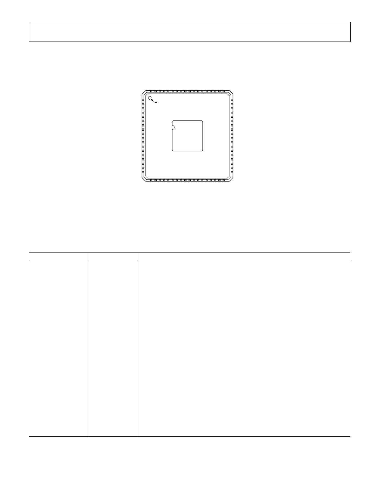
PIN CONFIGURATION AND FUNCTION DESCRIPTIONS
NC
AVDD
VCM C
AVDD
VIN – C
VIN + C
AVDD
AVDD
AVDDNCAVDD
AVDD
AVDD
VIN + B
VIN – B
AVDD
VCM B
AVDD
NC
TEMPOUT
RBIAS
AVDD
NC
NC
AVDD
VCM D
AVDD
VIN – D
VIN + D
AVDD
AVDD
AVDD
AVDD
CLK–
7271706968676665646362616059585756
1
2
3
4
5
6
7
8
9
10
11
12
13
14
15
16
17CLK+
18AVDD
PIN 1
INDICATOR
PIN 0 = EPAD = AGND
AD9639
TOP VIEW
(Not to S cale)
55
54
NC
53
PGM0
52
PGM1
51
PGM2
50
PGM3
49
NC
48
AVDD
47
VCM A
46
AVDD
45
VIN – A
44
VIN + A
43
AVDD
42
AVDD
41
AVDD
40
CSB
39
SCLK
38
SDI/SDIO
37
SDO
192021222324252627282930313233
NC
AVDD
AVDD
RESET
DRVDD
DRGND
DOUT – D
DOUT – C
DOUT + D
DOUT + C
NOTES
1. NC = NO CONNECT.
2. THE EXPOSED PADDLE MUST BE S OLDERED TO T HE GROUND PLANE
FOR THE L FCSP PACKAGE. S OLDERING T HE EXPOSED PADDLE TO
THE PCB INCREASES THE RELIABI LITY OF THE SOLDER JOINTS ,
MAXIMIZ ING THE THERM AL CAPABILITY OF THE PACKAGE.
DOUT + B
DOUT – B
34
35PDWN
36NC
DRVDD
DRGND
DOUT – A
DOUT + A
07973-004
Figure 3. Pin Configuration
Table 7. Pin Function Descriptions
Pin No. Mnemonic Description
0 AGND
Analog Ground (Exposed Paddle). The exposed paddle must be soldered to the ground
plane. Soldering the exposed paddle to the PCB increases the reliability of the solder joints,
maximizing the thermal capability of the package.
1, 5, 6, 19, 36, 49, 54,
NC No Connection.
63, 72
2 TEMPOUT Output Voltage to Monitor Temperature.
3 RBIAS External Resistor to Set the Internal ADC Core Bias Current.
4, 7, 9, 12, 13, 14, 15,
AVDD 1.8 V Analog Supply.
18, 20, 21, 41, 42, 43,
46, 48, 55, 57, 60, 61,
62, 64, 65, 66, 69, 71
8 VCM D Common-Mode Output Voltage Reference.
10 VIN − D ADC D Analog Input Complement.
11 VIN + D ADC D Analog Input True.
16 CLK− Clock Input Complement.
17 CLK+ Clock Input True.
22 RESET Reset Enable Pin. Resets the digital output timing.
23, 34 DRGND Digital Output Driver Ground.
24, 33 DRVDD 1.8 V Digital Output Driver Supply.
25 DOUT + D ADC D Digital Output True.
26 DOUT − D ADC D Digital Output Complement.
27 DOUT + C ADC C Digital Output True.
28 DOUT − C ADC C Digital Output Complement.
29 DOUT + B ADC B Digital Output True.
30 DOUT − B ADC B Digital Output Complement.
Rev. A | Page 9 of 36

AD9639
Pin No. Mnemonic Description
31 DOUT + A ADC A Digital Output True.
32 DOUT − A ADC A Digital Output Complement.
35 PDWN Power-Down.
37 SDO Serial Data Output for 4-Wire SPI Interface.
38 SDI/SDIO Serial Data Input/Serial Data Input/Output for 3-Wire SPI Interface.
39 SCLK Serial Clock.
40 CSB Chip Select Bar.
44 VIN + A ADC A Analog Input True.
45 VIN − A ADC A Analog Input Complement.
47 VCM A Common-Mode Output Voltage Reference.
50, 51, 52, 53
56 VCM B Common-Mode Output Voltage Reference.
58 VIN − B ADC B Analog Input Complement.
59 VIN + B ADC B Analog Input True.
67 VIN + C ADC C Analog Input True.
68 VIN − C ADC C Analog Input Complement.
70 VCM C Common-Mode Output Voltage Reference.
PGM3, PGM2,
PGM1, PGM0
Optional Pins to be Programmed by Customer.
Rev. A | Page 10 of 36
AD9639
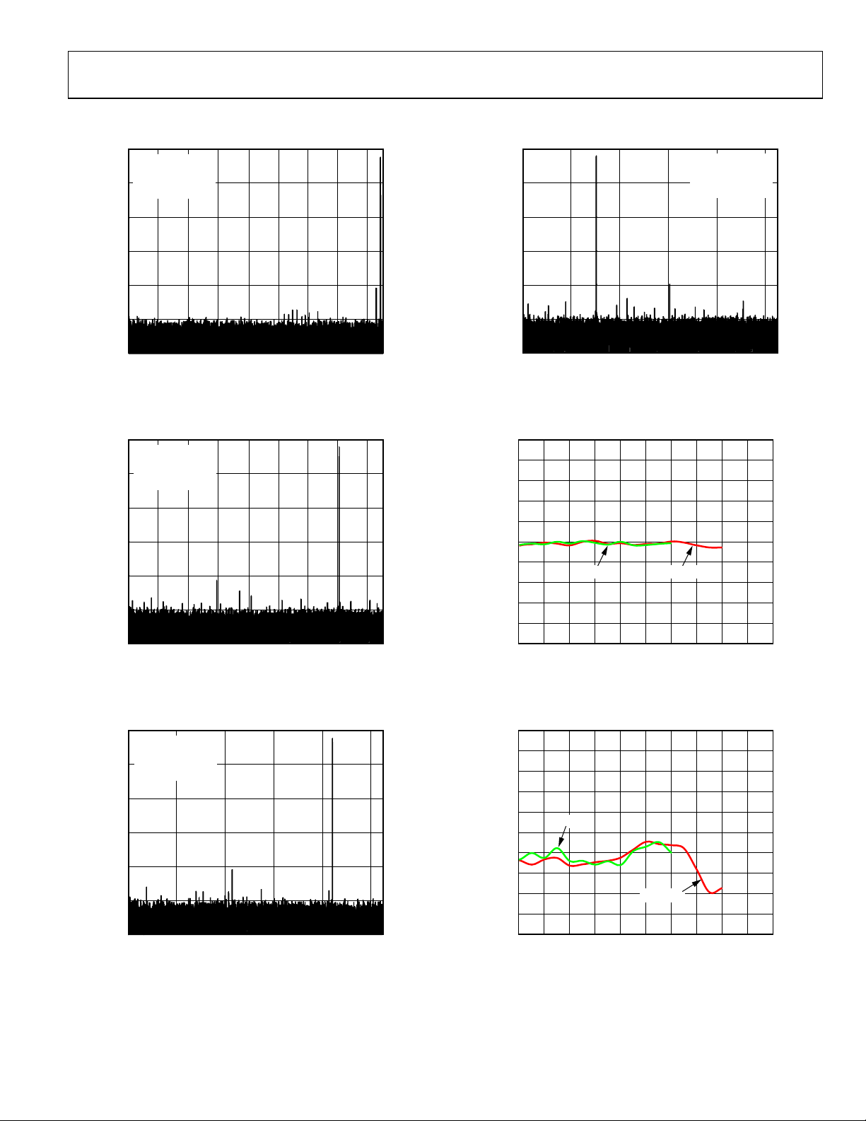
TYPICAL PERFORMANCE CHARACTERISTICS
0
AIN = –1.0dBFS
SNR = 64.88dB
ENOB = 10.49 BITS
–20
SFDR = 77.57d Bc
–20
0
AIN = –1.0dBFS
SNR = 63.13dB
ENOB = 10.19 BITS
SFDR = 76.07d Bc
–40
–60
–80
AMPLITUDE (dBFS)
–100
–120
01020304050607080
FREQUENCY (MHz)
Figure 4. Single-Tone 32k FFT with fIN = 84.3 MHz, f
0
AIN = –1.0dBFS
SNR = 63.95dB
ENOB = 10.33 BITS
–20
SFDR = 78.90d Bc
–40
–60
–80
AMPLITUDE (dBFS)
–100
–120
01020304050607080
FREQUENCY (MHz)
Figure 5. Single-Tone 32k FFT with fIN = 240.3 MHz, f
SAMPLE
SAMPLE
= 170 MSPS
= 170 MSPS
–40
–60
–80
AMPLITUDE (dBFS)
–100
–120
0 20 40 60 80 100
07973-059
Figure 7. Single-Tone 32k FFT with fIN = 240.3 MHz, f
70
69
68
67
66
65
64
SNR (dBFS)
63
62
61
60
50 70 90 110 130 150 170 190 210 230 250
07973-060
170MSPS
FREQUENCY (MHz)
210MSPS
ENCODE (MSPS)
SAMPLE
07973-062
= 210 MSPS
07973-067
Figure 8. SNR vs. Encode, fIN = 84.3 MHz
0
AIN = –1.0dBF S
SNR = 64.65dB
ENOB = 10.44 BITS
–20
SFDR = 77.54dBc
–40
–60
–80
AMPLITUDE ( dBFS)
–100
–120
0 20 40 60 80 100
FREQUENCY (MHz)
Figure 6. Single-Tone 32k FFT with fIN = 84.3 MHz, f
SAMPLE
= 210 MSPS
07973-061
Rev. A | Page 11 of 36
90
88
86
84
82
80
78
SFDR (dBFS)
76
74
72
70
170MSPS
210MSPS
50 70 90 110 130 150 170 190 210 230 250
ENCODE (MSPS)
Figure 9. SFDR vs. Encode, fIN = 84.3 MHz
07973-068
 Loading...