11-Bit, 105 MSPS/150 MSPS, 1.8 V
FEATURES
SNR = 65.8 dBc (66.8 dBFS) to 70 MHz @ 105 MSPS
SFDR = 85 dBc to 70 MHz @ 105 MSPS
Low power: 600 mW @ 105 MSPS
SNR = 65.7 dBc (66.7 dBFS) to 70 MHz @ 150 MSPS
SFDR = 84 dBc to 70 MHz @ 150 MSPS
Low power: 820 mW @ 150 MSPS
1.8 V analog supply operation
1.8 V to 3.3 V CMOS output supply or 1.8 V LVDS
output supply
Integer 1-to-8 input clock divider
IF sampling frequencies to 450 MHz
Internal ADC voltage reference
Integrated ADC sample-and-hold inputs
Flexible analog input range: 1 V p-p to 2 V p-p
Differential analog inputs with 650 MHz bandwidth
ADC clock duty cycle stabilizer
95 dB channel isolation/crosstalk
Serial port control
User-configurable, built-in self-test (BIST) capability
Energy-saving power-down modes
Integrated receive features
Fast detect/threshold bits
Composite signal monitor
APPLICATIONS
Communications
Diversity radio systems
Multimode digital receivers (3G)
GSM, EDGE, WCDMA, CDMA2000,
WiMAX, TD-SCDMA
I/Q demodulation systems
Smart antenna systems
General-purpose software radios
Broadband data applications
Dual Analog-to-Digital Converter
AD9627-11
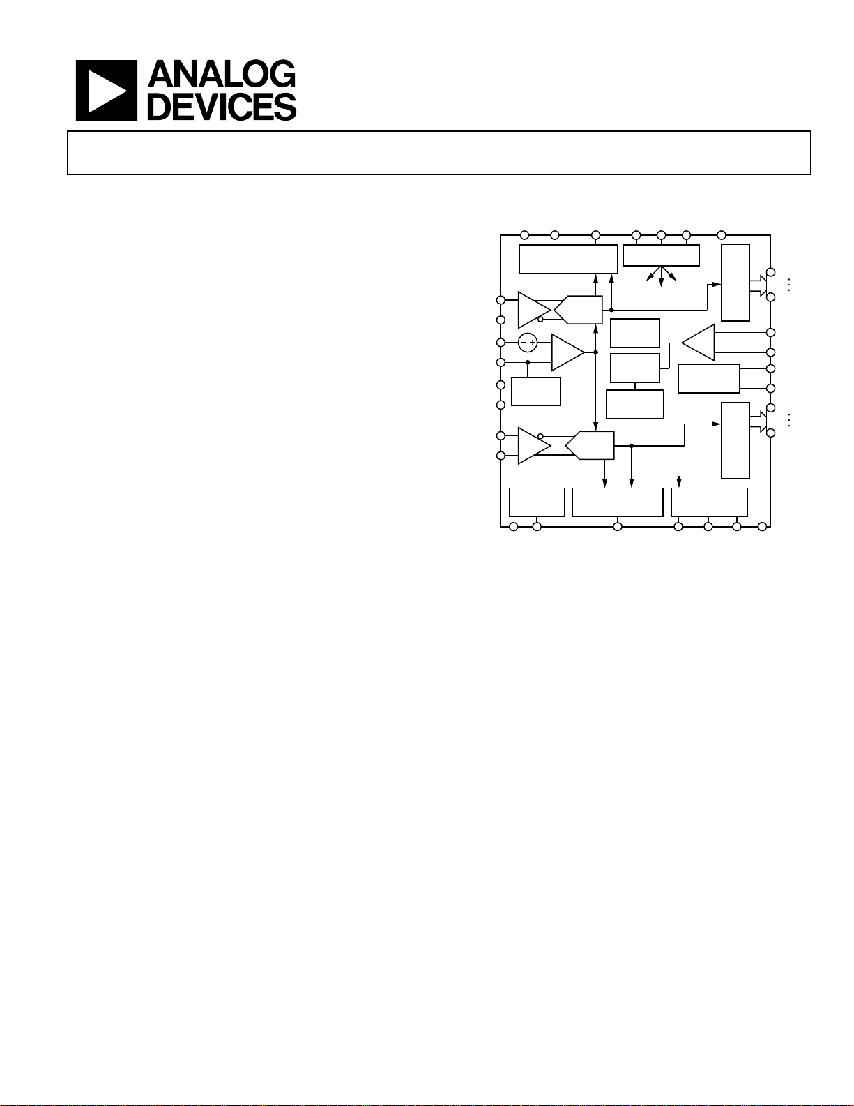
FUNCTIONAL BLOCK DIAGRAM
SCLK/
SDIO/
DCS
PROGRAMMING DATA
SIGNAL
MONITOR
DIVIDE
1 TO 8
DUTY CYCLE
STABILIZER
ADC
VIN+A
VIN–A
VREF
SENSE
CML
RBIAS
VIN–B
VIN+B
AVDD
DVDD
FD BITS/THRESHOLD
DETECT
SHA
REF
SELECT
SHA
ADC
FD(0:3)A
AD9627-11
MULTICHIP
SYNC
AGND SYNC FD(0:3)B
NOTES
1. PIN NAMES ARE FOR THE CMOS P IN CONFIG URATION ONL Y;
SEE FIGURE 7 FOR LVDS PIN NAMES.
FD BITS/THRESHOLD
DETECT
Figure 1.
PRODUCT HIGHLIGHTS
1. Integrated dual, 11-bit, 105 MSPS/150 MSPS ADC.
2. Fast overrange detect and signal monitor with serial output.
3. Signal monitor block with dedicated serial output mode.
4. Proprietary differential input that maintains excellent SNR
performance for input frequencies up to 450 MHz.
5. Operation from a single 1.8 V supply and a separate digital
output driver supply to accommodate 1.8 V to 3.3 V logic
families.
6. Standard serial port interface (SPI) that supports various
product features and functions, such as data formatting
(offset binary, twos complement, or gray coding), enabling
the clock DCS, power-down, test modes, and voltage
reference mode.
7. Pin compatibility with the AD9640, AD9627, and AD9600
for a simple migration from 11 bits to 14 bits, 12 bits, or
10 bits.
CSB
DFS
SPI
DCO
GENERATION
SIGNAL MO NITOR
DATA
SIGNAL MO NITOR
INTERFACE
SMI
SMI
SCLK/
SDFS
PDWN
DRVDD
CMOS
CMOS
SMI
SDO/
OEB
D10A
D0A
OUTPUT BUFFER
CLK+
CLK–
DCOA
DCOB
D10B
D0B
OUTPUT BUFFER
DRGND
07054-001
Rev. B
Information furnished by Analog Devices is believed to be accurate and reliable. However, no
responsibility is assumed by Analog Devices for its use, nor for any infringements of patents or other
rights of third parties that may result from its use. Specifications subject to change without notice. No
license is granted by implication or otherwise under any patent or patent rights of Analog Devices.
Trademarks and registered trademarks are the property of their respective owners.
One Technology Way, P.O. Box 9106, Norwood, MA 02062-9106, U.S.A.
Tel: 781.329.4700 www.analog.com
Fax: 781.461.3113 ©2007–2010 Analog Devices, Inc. All rights reserved.
 Loading...