

12-Bit, 170 MSPS/210 MSPS/250 MSPS,
V
A
V
1.8 V Dual Analog-to-Digital Converter (ADC)
Data Sheet
FEATURES
SNR = 69.6 dBFS at 185 MHz fIN and 250 MSPS
SFDR = 86 dBc at 185 MHz f
−149.9 dBFS/Hz input noise at 185 MHz, −1 dBFS A
250 MSPS
Total power consumption: 770 mW at 250 MSPS
1.8 V supply voltages
LVDS (ANSI-644 levels) outputs
Integer 1-to-8 input clock divider (625 MHz maximum input)
Sample rates of up to 250 MSPS
IF sampling frequencies of up to 400 MHz
Internal ADC voltage reference
Flexible analog input range
1.4 V p-p to 2.0 V p-p (1.75 V p-p nominal)
ADC clock duty cycle stabilizer
95 dB channel isolation/crosstalk
Serial port control
Energy-saving power-down modes
User-configurable, built-in self test (BIST) capability
APPLICATIONS
Communications
Diversity radio systems
Multimode digital receivers (3G)
TD-SCDMA, WiMAX, W-CDMA, CDMA2000, GSM, EDGE, LTE
I/Q demodulation systems
Smart antenna systems
General-purpose software radios
Ultrasound equipment
Broadband data applications
GENERAL DESCRIPTION
The AD9613 is a dual 12-bit, analog-to-digital converter (ADC)
with sampling speeds of up to 250 MSPS. The AD9613 is designed
to support communications applications where low cost, small
size, wide bandwidth, and versatility are desired.
The dual ADC cores feature a multistage, differential pipelined
architecture with integrated output error correction logic. Each
ADC features wide bandwidth inputs supporting a variety of userselectable input ranges. An integrated voltage reference eases design
considerations. A duty cycle stabilizer (DCS) is provided to
compensate for variations in the ADC clock duty cycle,
allowing the converters to maintain excellent performance.
The ADC output data is routed directly to the two external 12-bit
LVDS output ports and formatted as either interleaved or channel
multiplexed.
Flexible power-down options allow significant power savings,
when desired.
Rev. B
Information furnished by Analog Devices is believed to be accurate and reliable. However, no
responsibility is assumed by Anal og Devices for its use, nor for any infringements of patents or ot her
rights of third parties that may result from its use. Specifications subject to change without notice. No
license is granted by implication or otherwise under any patent or patent rights of Analog Devices.
Trademarks and registered trademarks are the property of their respective owners.
and 250 MSPS
IN
and
IN
AD9613
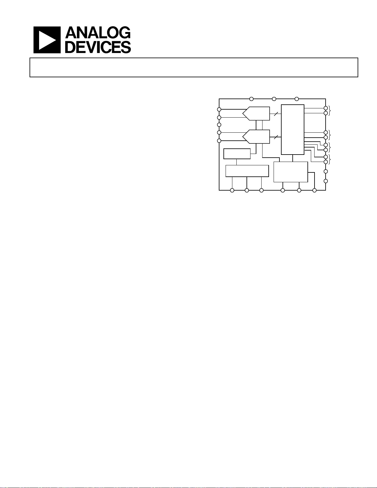
FUNCTIONAL BLOCK DIAGRAM
DD AGND DRVDD
VIN+A
VIN–A
VCM
IN+B
VIN–B
NOTES
1. THE D0± TO D11± PINS REPRESENT BOTH THE CHANNEL A
AD9613
REFERENCE
SCLK SDIO CSB CLK+ CLK– SYNC
AND CHANNE L B LVDS OUTPUT DATA.
Programming for setup and control is accomplished using a
3-wire SPI-compatible serial interface.
The AD9613 is available in a 64-lead LFCSP and is specified
over the industrial temperature range of −40°C to +85°C. This
product is protected by a U.S. patent.
PRODUCT HIGHLIGHTS
1. Integrated dual, 12-bit, 170 MSPS/210 MSPS/250 MSPS ADCs.
2. Fast overrange and threshold detect.
3. Proprietary differential input maintains excellent SNR
performance for input frequencies of up to 400 MHz.
4. SYNC input allows synchronization of multiple devices.
5. 3-pin, 1.8 V SPI port for register programming and register
readback.
6. Pin compatibility with the AD9643, allowing a simple
migration up to 14 bits, and with the AD6649 and the AD6643.
One Technology Way, P.O. Box 9106, Norwood, MA 02062-9106, U.S.A.
Tel: 781.329.4700 www.analog.com
Fax: 781.461.3113 ©2011 Analog Devices, Inc. All rights reserved.
PIPELINE
12-BIT
ADC
PIPELINE
12-BIT
ADC
SERIAL PORT
12
PARALLEL
DDR LVDS
12
DRIVERS
CLOCK
DIVIDER
Figure 1.
AND
1TO 8
D0±
D11±
DCO±
OR±
OEB
PDWN
.
.
.
.
.
09637-001

AD9613 Data Sheet
TABLE OF CONTENTS
Features.............................................................................................. 1
Applications....................................................................................... 1
General Description ......................................................................... 1
Functional Block Diagram .............................................................. 1
Product Highlights ........................................................................... 1
Revision History ............................................................................... 2
Specifications..................................................................................... 3
ADC DC Specifications ............................................................... 3
ADC AC Specifications ............................................................... 4
Digital Specifications ................................................................... 6
Switching Specifications.............................................................. 8
Timing Specifications .................................................................. 9
Absolute Maximum Ratings.......................................................... 11
Thermal Characteristics ............................................................11
ESD Caution................................................................................ 11
Pin Configurations and Function Descriptions ......................... 12
Typical Performance Characteristics ........................................... 16
Equivalent Circuits......................................................................... 22
Theory of Operation ...................................................................... 23
ADC Architecture ......................................................................23
REVISION HISTORY
9/11—Rev. A to Rev. B
Changes to Figure 1.......................................................................... 1
Changes to Temperature Drift Parameters ................................... 3
Changes Output Offset Voltage (V
Parameter and Output Offset Voltage (V
Mode Parameter................................................................................ 7
Changes to Output Enable Bar and Power-Down Pin Type
and Pin 47 Description .................................................................. 13
Changes to Figure 5 and Pin 7 and Pin 8 Descriptions............. 14
Changes to Pin 42 and Pin 43, Output Enable Bar and Power-
Down Pin Type, and Pin 47 Descriptions ................................... 15
Changes to Typical Performance Characteristics Conditions .. 16
Changes to Fiugre 43...................................................................... 22
Added ADC Overrange (OR) Section ......................................... 27
), ANSI Mode Typ
OS
), Reduced Swing
OS
Analog Input Considerations ................................................... 23
Voltage Reference....................................................................... 25
Clock Input Considerations...................................................... 25
Power Dissipation and Standby Mode .................................... 27
Digital Outputs........................................................................... 27
ADC Overrange (OR)................................................................ 27
Channel/Chip Synchronization.................................................... 28
Serial Port Interface (SPI).............................................................. 29
Configuration Using the SPI..................................................... 29
Hardware Interface..................................................................... 29
SPI Accessible Features.............................................................. 30
Memory Map .................................................................................. 31
Reading the Memory Map Register Table............................... 31
Memory Map Register Table..................................................... 32
Memory Map Register Description ......................................... 34
Applications Information.............................................................. 35
Design Guidelines ...................................................................... 35
Outline Dimensions....................................................................... 36
Ordering Guide .......................................................................... 36
Changes to Channel/Chip Synchronization Section................. 28
Changes to Reading the Memory Map Register Table
Section and Transfer Register Map Section ................................ 31
Changes to Register 0x02, Bits[5:4] ............................................. 32
Changes to Register 0x16, Bit 5 .................................................... 33
Added Register 0x3A ..................................................................... 34
Deleted Register 0x59 .................................................................... 34
Changes to Bit 0—Master Sync Buffer Enable Section ............. 34
Deleted SYNC Pin Control (Register 0x59) Section.................. 34
5/11—Rev. 0 to Rev. A
Changes to Table 2, AD9613-170: Worst Second or Third
Harmonic and Worst Other (Harmonic or Spur) Max Values
and Spurious Free Dynamic Range Min Value .............................4
4/11—Revision 0: Initial Version
Rev. B | Page 2 of 36

Data Sheet AD9613
SPECIFICATIONS
ADC DC SPECIFICATIONS
AVDD = 1.8 V, DRVDD = 1.8 V, maximum sample rate, VIN = −1.0 dBFS differential input, 1.75 V p-p full scale input range, DCS enabled,
unless otherwise noted.
Table 1.
AD9613-170 AD9613-210 AD9613-250
Parameter Temp Min Typ Max Min Typ Max Min Typ Max Unit
RESOLUTION Full 12 12 12 Bits
ACCURACY
No Missing Codes Full Guaranteed Guaranteed Guaranteed
Offset Error Full ±10 ±10 ±10 mV
Gain Error Full +2/−6 +3/−5 ±4 %FSR
Differential Nonlinearity (DNL) Full ±0.5 ±0.5 ±0.5 LSB
25°C ±0.25 ±0.25 ±0.25 LSB
Integral Nonlinearity (INL)1 Full ±0.5 ±0.6 ±0.8 LSB
25°C ±2.0 ±2.0 ±2.0 LSB
MATCHING CHARACTERISTIC
Offset Error Full ±13 ±13 ±13 mV
Gain Error Full ±2.5 +3.5/−2 +3.5/−2.5 %FSR
TEMPERATURE DRIFT
Offset Error Full ±5 ±5 ±5 ppm/°C
Gain Error Full ±70 ±80 ±100 ppm/°C
INPUT-REFERRED NOISE
VREF = 1.0 V 25°C 0.39 0.39 0.39 LSB rms
ANALOG INPUT
Input Span Full 1.75 1.75 1.75 V p-p
Input Capacitance2 Full 2.5 2.5 2.5 pF
Input Resistance3 Full 20 20 20 kΩ
Input Common-Mode Voltage Full 0.9 0.9 0.9 V
POWER SUPPLIES
Supply Voltage
AVDD Full 1.7 1.8 1.9 1.7 1.8 1.9 1.7 1.8 1.9 V
DRVDD Full 1.7 1.8 1.9 1.7 1.8 1.9 1.7 1.8 1.9 V
Supply Current
1
I
Full 230 250 241 265 252 275 mA
AVDD
1
I
Full 142 160 159 185 176 210 mA
DRVDD
POWER CONSUMPTION
Sine Wave Input1 (DRVDD = 1.8 V) Full 670 738 720 810 770 873 mW
Standby Power4 Full 90 90 90 mW
Power-Down Power Full 10 10 10 mW
1
Measured with a low input frequency, full-scale sine wave.
2
Input capacitance refers to the effective capacitance between one differential input pin and its complement.
3
Input resistance refers to the effective resistance between one differential input pin and its complement.
4
Standby power is measured with a dc input and the CLK± pin inactive (that is, set to AVDD or AGND).
Rev. B | Page 3 of 36

AD9613 Data Sheet
ADC AC SPECIFICATIONS
AVDD = 1.8 V, DRVDD = 1.8 V, maximum sample rate, VIN = −1.0 dBFS differential input, 1.75 V p-p full scale input range, unless
otherwise noted.
Table 2.
AD9613-170 AD9613-210 AD9613-250
Parameter1 Temp Min Typ Max Min Typ Max Min Typ Max Unit
SIGNAL-TO-NOISE-RATIO (SNR)
fIN = 30 MHz 25°C 70.1 70.1 70.0 dBFS
fIN = 90 MHz 25°C 70.0 70.0 69.8 dBFS
Full 69.3 69.2 dBFS
fIN = 140 MHz 25°C 69.8 69.8 69.6 dBFS
fIN = 185 MHz 25°C 69.5 69.5 69.2 dBFS
Full 67.8 dBFS
fIN = 220 MHz 25°C 69.4 69.3 69.0 dBFS
SIGNAL-TO-NOISE AND DISTORTION (SINAD)
fIN = 30 MHz 25°C 69.1 69.1 69.0 dBFS
fIN = 90 MHz 25°C 69.0 69.0 68.8 dBFS
Full 68.2 68 dBFS
fIN = 140 MHz 25°C 68.8 68.8 68.6 dBFS
fIN = 185 MHz 25°C
Full 66.5 dBFS
fIN = 220 MHz 25°C
EFFECTIVE NUMBER OF BITS (ENOB)
fIN = 30 MHz
fIN = 90 MHz
fIN = 140 MHz
fIN = 185 MHz
fIN = 220 MHz
WORST SECOND OR THIRD HARMONIC
fIN = 30 MHz
fIN = 90 MHz
fIN = 140 MHz
fIN = 185 MHz
fIN = 220 MHz
SPURIOUS-FREE DYNAMIC RANGE (SFDR)
fIN = 30 MHz
fIN = 90 MHz
fIN = 140 MHz
fIN = 185 MHz
fIN = 220 MHz
WORST OTHER (HARMONIC OR SPUR)
fIN = 30 MHz
fIN = 90 MHz
fIN = 140 MHz
fIN = 185 MHz
fIN = 220 MHz
25°C
25°C
25°C
25°C
25°C
25°C
25°C
Full
25°C
25°C
Full
25°C
25°C
25°C
Full
25°C
25°C
Full
25°C
25°C
25°C
Full
25°C
25°C
Full
25°C
68.5
68.4
11.2
−94 −94 −90
−92 −94 −89
−78 −80
−87 −88 −86
−89 −83 −86
−80
−80 −83 −85
94 90 92
92 90 89
78 80
87 88 86
89 83 86
80
83 83 85
−97 −95 −93
−96 −95 −92
−78 −80
−97 −97 −91
−91 −96 −91
−80
−93 −94 −89
11.2
11.1
11.1
11.1
68.5
68.3
11.2
11.2
11.1
11.1
11.0
68.2
68.0
11.2
11.1
11.1
11.0
11.0
dBFS
dBFS
Bits
Bits
Bits
Bits
Bits
dBc
dBc
dBc
dBc
dBc
dBc
dBc
dBc
dBc
dBc
dBc
dBc
dBc
dBc
dBc
dBc
dBc
dBc
dBc
dBc
dBc
Rev. B | Page 4 of 36

Data Sheet AD9613
AD9613-170 AD9613-210 AD9613-250
Parameter1 Temp Min Typ Max Min Typ Max Min Typ Max Unit
TWO-TONE SFDR
fIN = 184.12 MHz (−7 dBFS),
25°C
88 88 88
187.12 MHz (−7 dBFS)
CROSSTALK2
Full
95 95 95
FULL POWER BANDWIDTH3 25°C 400 400 400 MHz
NOISE BANDWIDTH4 25°C 1000 1000 1000 MHz
1
See the AN-835 Application Note, Understanding High Speed ADC Testing and Evaluation, for a complete set of definitions.
2
Crosstalk is measured at 100 MHz with −1.0 dBFS on one channel and no input on the alternate channel.
3
Full power bandwidth is the bandwidth of operation where typical ADC performance can be achieved.
4
Noise bandwidth is the −3 dB bandwidth for the ADC inputs across which noise can enter the ADC and is not attenuated internally.
dBc
dB
Rev. B | Page 5 of 36

AD9613 Data Sheet
DIGITAL SPECIFICATIONS
AVDD = 1.8 V, DRVDD = 1.8 V, maximum sample rate, VIN = −1.0 dBFS differential input, 1.75 V p-p full-scale input range, DCS enabled,
unless otherwise noted.
Table 3.
Parameter Te mp Min Typ Max Unit
DIFFERENTIAL CLOCK INPUTS (CLK+, CLK−)
Logic Compliance CMOS/LVDS/LVPECL
Internal Common-Mode Bias Full 0.9 V
Differential Input Voltage
Input Voltage Range
Input Common-Mode Range
High Level Input Current Full 10 22 μA
Low Level Input Current Full −22 −10 μA
Input Capacitance
Input Resistance
SYNC INPUT
Logic Compliance CMOS/LVDS
Internal Bias Full 0.9 V
Input Voltage Range Full AGND AVDD V
High Level Input Voltage Full 1.2 AVDD V
Low Level Input Voltage Full AGND 0.6 V
High Level Input Current Full −5 +5 μA
Low Level Input Current Full −5 +5 μA
Input Capacitance Full 1 pF
Input Resistance Full 12 16 20 kΩ
LOGIC INPUT (CSB)1
High Level Input Voltage Full 1.22 2.1 V
Low Level Input Voltage Full 0 0.6 V
High Level Input Current Full −5 +5 μA
Low Level Input Current Full −80 +45 μA
Input Resistance Full 26 kΩ
Input Capacitance Full 2 pF
LOGIC INPUT (SCLK)2
High Level Input Voltage Full 1.22 2.1 V
Low Level Input Voltage Full 0 0.6 V
High Level Input Current Full 45 70 μA
Low Level Input Current Full −5 +5 μA
Input Resistance Full 26 kΩ
Input Capacitance Full 2 pF
LOGIC INPUTS (SDIO)1
High Level Input Voltage Full 1.22 2.1 V
Low Level Input Voltage Full 0 0.6 V
High Level Input Current Full 45 70 μA
Low Level Input Current Full −5 +5 μA
Input Resistance Full 26 kΩ
Input Capacitance Full 5 pF
Full 0.3
Full AGND
Full 0.9
Full 4
Full 8 10 12
3.6
AVDD
1.4
V p-p
V
V
pF
kΩ
Rev. B | Page 6 of 36

Data Sheet AD9613
Parameter Te mp Min Typ Max Unit
LOGIC INPUTS (OEB, PDWN)2
High Level Input Voltage Full 1.22 2.1 V
Low Level Input Voltage Full 0 0.6 V
High Level Input Current Full 45 70 μA
Low Level Input Current Full −5 +5 μA
Input Resistance Full 26 kΩ
Input Capacitance Full 5 pF
DIGITAL OUTPUTS
LVDS Data and OR Outputs
Differential Output Voltage (VOD), ANSI Mode Full 250 350 450 mV
Output Offset Voltage (VOS), ANSI Mode Full 1.15 1.22 1.35 V
Differential Output Voltage (VOD), Reduced Swing Mode Full 150 200 280 mV
Output Offset Voltage (VOS), Reduced Swing Mode Full 1.15 1.22 1.35 V
1
Pull up.
2
Pull down.
Rev. B | Page 7 of 36

AD9613 Data Sheet
SWITCHING SPECIFICATIONS
Table 4.
AD9613-170 AD9613-210 AD9613-250
Parameter Temp Min Typ Max Min Typ Max Min Typ Max Unit
CLOCK INPUT PARAMETERS
Input Clock Rate Full 625 625 625 MHz
Conversion Rate1 Full 40 170 40 210 40 250 MSPS
CLK Period, Divide-by-1 Mode (t
CLK Pulse Width High (tCH)
Divide-by-1 Mode, DCS Enabled Full 2.61 2.9 3.19 2.16 2.4 2.64 1.8 2.0 2.2 ns
Divide-by-1 Mode, DCS Disabled Full 2.76 2.9 3.05 2.28 2.4 2.52 1.9 2.0 2.1 ns
Divide-by-2 Mode Through Divide-by-8 Mode Full 0.8
Aperture Delay (tA) Full 1.0 1.0 1.0 ns
Aperture Uncertainty (Jitter, tJ) Full 0.1 0.1 0.1 ps rms
DATA OUTPUT PARAMETERS
LVDS Mode
Data Propagation Delay (tPD) Full
DCO Propagation Delay (t
DCO to Data Skew (t
SKEW
Pipeline Delay (Latency) Full 10 10 10 Cycles
Aperture Delay (tA) Full 1.0 1.0 1.0 ns
Aperture Uncertainty (Jitter, tJ) Full 0.1 0.1 0.1 ps rms
Wake-Up Time (from Standby) Full 10 10 10 μs
Wake-Up Time (from Power Down) Full 250 250 250 μs
Out-of-Range Recovery Time Full 3 3 3 Cycles
1
Conversion rate is the clock rate after the divider.
) Full 5.8 4.8 4 ns
CLK
4.8 4.8 4.8
) Full
DCO
5.5 5.5 5.5
0.8
0.8
ns
ns
ns
) Full 0.3 0.7 1.1 0.3 0.7 1.1 0.3 0.7 1.1 ns
Rev. B | Page 8 of 36

Data Sheet AD9613
TIMING SPECIFICATIONS
Table 5.
Parameter Test Conditions/Comments Min Typ Max Unit
SYNC TIMING REQUIREMENTS See Figure 3 for timing details
t
SYNC to the rising edge of CLK setup time 0.3 ns
SSYNC
t
SYNC to the rising edge of CLK hold time 0.4 ns
HSYNC
SPI TIMING REQUIREMENTS See Figure 58 for SPI timing diagram
tDS Setup time between the data and the rising edge of SCLK 2 ns
tDH Hold time between the data and the rising edge of SCLK 2 ns
t
Period of the SCLK 40 ns
CLK
tS Setup time between CSB and SCLK 2 ns
tH Hold time between CSB and SCLK 2 ns
t
Minimum period that SCLK should be in a logic high state 10 ns
HIGH
t
Minimum period that SCLK should be in a logic low state 10 ns
LOW
t
EN_SDIO
t
DIS_SDIO
Time required for the SDIO pin to switch from an input to an output
relative to the SCLK falling edge (not shown in Figure 58)
Time required for the SDIO pin to switch from an output to an input
relative to the SCLK rising edge (not shown in Figure 58)
10 ns
10 ns
Rev. B | Page 9 of 36

AD9613 Data Sheet
Timing Diagrams
t
A
N
N + 1
t
CLK
t
DCO
t
t
SKEW
PD
CH A
CH B
N – 10
N – 10
CH A
CH B
N – 10
N – 10
CH A
N – 9
CH A
N – 9
N + 2
CH B
N – 9
CH B
N – 9
CH A
N – 8
CH A
N – 8
N + 3
CH B
N – 8
CH B
N – 8
CH A
N – 7
CH A
N – 7
N + 4
CH B
N – 7
CH B
N – 7
CH A
N – 6
CH A
N – 6
N + 5
PARALLEL INTERLEAVED
CHANNEL A AND
CHANNEL B
VIN
CLK+
CLK–
DCO–
DCO+
(MSB)
D0±
(LSB)
.
.
.
D11±
N – 1
t
CH
CHANNEL MULTIP LEXED
(EVEN/ODD) M ODE
CHANNEL MULTIP LEXED
(EVEN/ODD) M ODE
D0±/D1±
CHANNEL A
D10±/D11±
D0±/D1±
CHANNEL B
D10±/D11±
(LSB)
(MSB)
(LSB)
(MSB)
CH A0
CH A1
CH A0
CH A1
CH A0
CH A1
CH A0
CH A1
N – 10
CH A10
N – 10
CH B0
N – 10
CH B10
N – 10
N – 10
CH A11
N – 10
CH B1
N – 10
CH B11
N – 10
.
.
.
.
.
.
N – 9
CH A10
N – 9
CH B0
N – 9
CH B10
N – 9
N – 9
CH A11
N – 9
CH B1
N – 9
CH B11
N – 9
N – 8
CH A10
N – 8
CH B0
N – 8
CH B10
N – 8
N – 8
CH A11
N – 8
CH B1
N – 8
CH B11
N – 8
N – 7
CH A10
N – 7
CH B0
N – 7
CH B10
N – 7
N – 7
CH A11
N – 7
CH B1
N – 7
CH B11
N – 7
CH A0
N – 6
CH A10
N – 6
CH B0
N – 6
CH B10
N – 6
09637-002
Figure 2. Interleaved LVDS Mode Data Output Timing
CLK+
SYNC
t
SSYNC
t
HSYNC
09637-003
Figure 3. SYNC Timing Inputs
Rev. B | Page 10 of 36

Data Sheet AD9613
ABSOLUTE MAXIMUM RATINGS
Table 6.
Parameter Rating
Electrical
AVDD to AGND −0.3 V to +2.0 V
DRVDD to AGND −0.3 V to +2.0 V
VIN+A/VIN+B, VIN−A/VIN−B to AGND −0.3 V to AVDD + 0.2 V
CLK+, CLK− to AGND −0.3 V to AVDD + 0.2 V
SYNC to AGND −0.3 V to AVDD + 0.2 V
VCM to AGND −0.3 V to AVDD + 0.2 V
CSB to AGND −0.3 V to DRVDD + 0.3 V
SCLK to AGND −0.3 V to DRVDD + 0.3 V
SDIO to AGND −0.3 V to DRVDD + 0.3 V
OEB to AGND −0.3 V to DRVDD + 0.3 V
PDWN to AGND −0.3 V to DRVDD + 0.3 V
OR+/OR− to AGND −0.3 V to DRVDD + 0.3 V
D0−/D0+ Through D11−/D11+ to
−0.3 V to DRVDD + 0.3 V
AGND
DCO+/DCO− to AGND −0.3 V to DRVDD + 0.3 V
Environmental
Operating Temperature Range
−40°C to +85°C
(Ambient)
Maximum Junction Temperature
150°C
Under Bias
Storage Temperature Range
−65°C to +125°C
(Ambient)
Stresses above those listed under Absolute Maximum Ratings
may cause permanent damage to the device. This is a stress
rating only; functional operation of the device at these or any
other conditions above those indicated in the operational
section of this specification is not implied. Exposure to absolute
maximum rating conditions for extended periods may affect
device reliability.
THERMAL CHARACTERISTICS
The exposed paddle must be soldered to the ground plane for
the LFCSP package. Soldering the exposed paddle to the
printed circuit board (PCB) increases the reliability of the
solder joints, maximizing the thermal capability of the package.
Typical θ
is specified for a 4-layer PCB with solid ground
JA
plane. As shown in Figure 40, airflow increases heat dissipation,
which reduces θ
. In addition, metal in direct contact with the
JA
package leads from metal traces, through holes, ground, and
power planes reduces the θ
.
JA
Table 7. Thermal Resistance
Airflow
Vel ocit y
Packa ge Type
64-Lead LFCSP
9 mm × 9 mm
(CP-64-4)
1
Per JEDEC 51-7, plus JEDEC 25-5 2S2P test board.
2
Per JEDEC JESD51-2 (still air) or JEDEC JESD51-6 (moving air).
3
Per MIL-Std 883, Method 1012.1.
4
Per JEDEC JESD51-8 (still air).
(m/sec) θ
0 26.8 1.14 10.4 °C/W
1.0 21.6 °C/W
2.0 20.2 °C/W
1, 2
1, 3
θ
JA
JC
1, 4
θ
Unit
JB
ESD CAUTION
Rev. B | Page 11 of 36
 Loading...