ANALOG DEVICES AD9601 Service Manual

10-Bit, 200 MSPS/250 MSPS
FEATURES
SNR = 59.4 dBFS @ fIN up to 70 MHz @ 250 MSPS
ENOB of 9.7 @ f
SFDR = 81 dBc @ f
Excellent linearity
DNL = 0.2 LSB typical
INL = 0.2 LSB typical
CMOS outputs
Single data port at up to 250 MHz
Demultiplexed dual port at up to 2 × 125 MHz
700 MHz full power analog bandwidth
On-chip reference, no external decoupling required
Integrated input buffer and track-and-hold
Low power dissipation
274 mW @ 200 MSPS
322 mW @ 250 MSPS
Programmable input voltage range
1.0 V to 1.5 V, 1.25 V nominal
1.8 V analog and digital supply operation
Selectable output data format (offset binary, twos
complement, Gray code)
Clock duty cycle stabilizer
Integrated data capture clock
up to 70 MHz @ 250 MSPS (−1.0 dBFS)
IN
up to 70 MHz @ 250 MSPS (−1.0 dBFS)
IN
1.8 V Analog-to-Digital Converter
AD9601
APPLICATIONS
Wireless and wired broadband communications
Cable reverse path
Communications test equipment
Radar and satellite subsystems
Power amplifier linearization
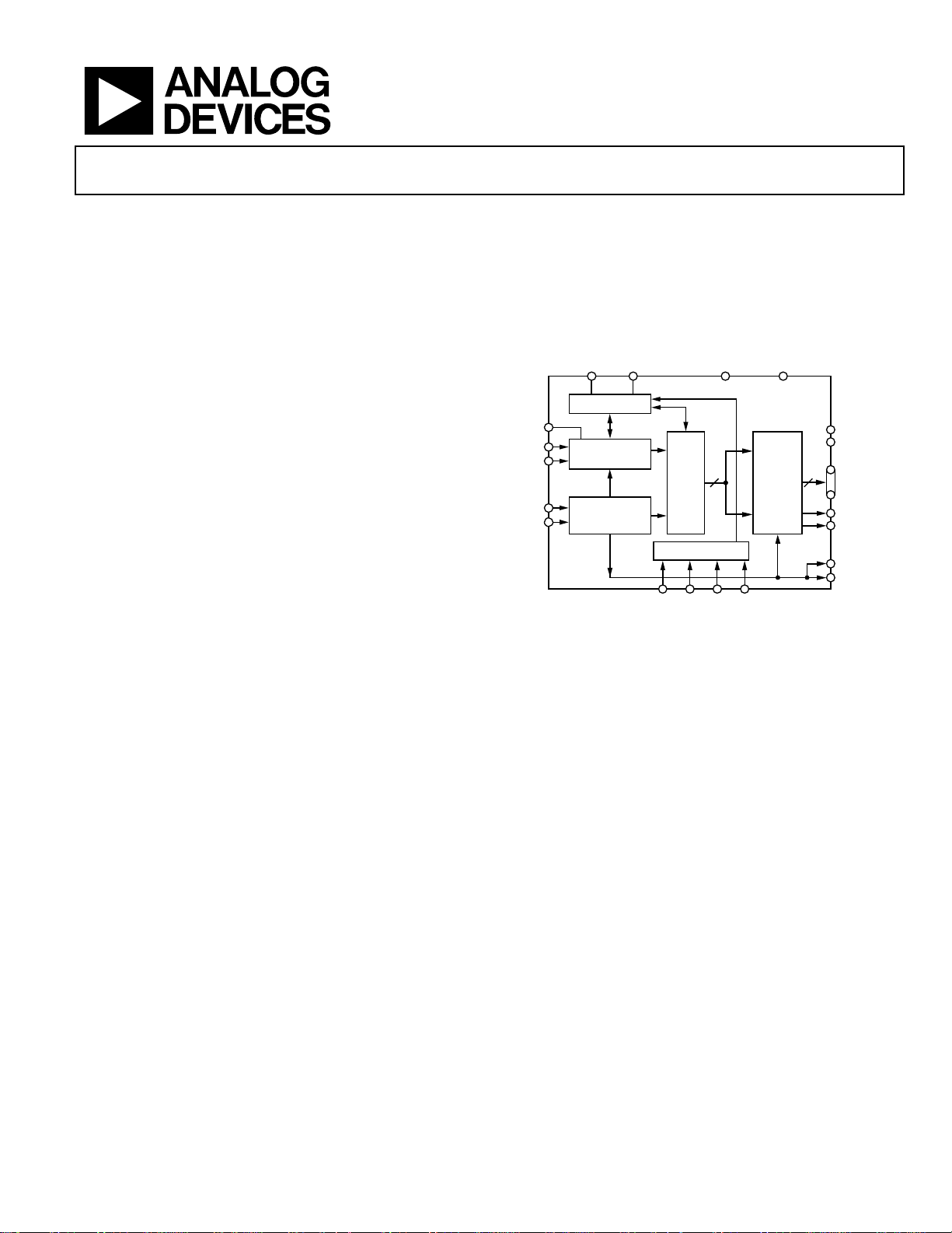
FUNCTIONAL BLOCK DIAGRAM
AGNDPWDNRBIAS AVDD (1.8V)
CML
VIN+
VIN–
CLK+
CLK–
REFERENCE
TRACK-AND-HOLD
CLOCK
MANAGEMENT
ADC
10-BIT
CORE
SERIAL PORT
RESET
SCLK SDIO CSB
10 10
Figure 1.
AD9601
OUTPUT
STAGING
LVDS
DRVDD
DRGND
Dx9 TO Dx0
OVRA
OVRB
DCO+
DCO–
07100-001
GENERAL DESCRIPTION
The AD9601 is a 10-bit monolithic sampling analog-to-digital
converter optimized for high performance, low power, and ease
of use. The product operates at up to a 250 MSPS conversion
rate and is optimized for outstanding dynamic performance in
wideband carrier and broadband systems. All necessary functions, including a track-and-hold (T/H) and voltage reference,
are included on the chip to provide a complete signal
conversion solution.
The ADC requires a 1.8 V analog voltage supply and a differential clock for full performance operation. The digital outputs are
CMOS compatible and support either twos complement, offset
binary format, or Gray code. A data clock output is available for
proper output data timing.
Fabricated on an advanced CMOS process, the AD9601 is
available in a 56-lead LFCSP, specified over the industrial
temperature range (−40°C to +85°C).
Rev. 0
Information furnished by Analog Devices is believed to be accurate and reliable. However, no
responsibility is assumed by Anal og Devices for its use, nor for any infringements of patents or ot her
rights of third parties that may result from its use. Specifications subject to change without notice. No
license is granted by implication or otherwise under any patent or patent rights of Analog Devices.
Trademarks and registered trademarks are the property of their respective owners.
PRODUCT HIGHLIGHTS
1. High Performance—Maintains 59.4 dBFS SNR @ 250 MSPS
with a 70 MHz input.
2. Low Power—Consumes only 322 mW @ 250 MSPS.
3. Ease of Use—CMOS output data and output clock signal
allow interface to current FPGA technology. The on-chip
reference and sample-and-hold provide flexibility in
system design. Use of a single 1.8 V supply simplifies
system power supply design.
4. Serial Port Control—Standard serial port interface supports
various product functions, such as data formatting, powerdown, gain adjust, and output test pattern generation.
5. Pin-Compatible Family—12-bit pin-compatible family
offered as the AD9626.
One Technology Way, P.O. Box 9106, Norwood, MA 02062-9106, U.S.A.
Tel: 781.329.4700 www.analog.com
Fax: 781.461.3113 ©2007 Analog Devices, Inc. All rights reserved.

AD9601
TABLE OF CONTENTS
Features .............................................................................................. 1
Applications....................................................................................... 1
Functional Block Diagram .............................................................. 1
General Description......................................................................... 1
Product Highlights ........................................................................... 1
Revision History ............................................................................... 2
Specifications..................................................................................... 3
DC Specifications ......................................................................... 3
AC Specifications.......................................................................... 4
Digital Specifications ................................................................... 5
Switching Specifications .............................................................. 6
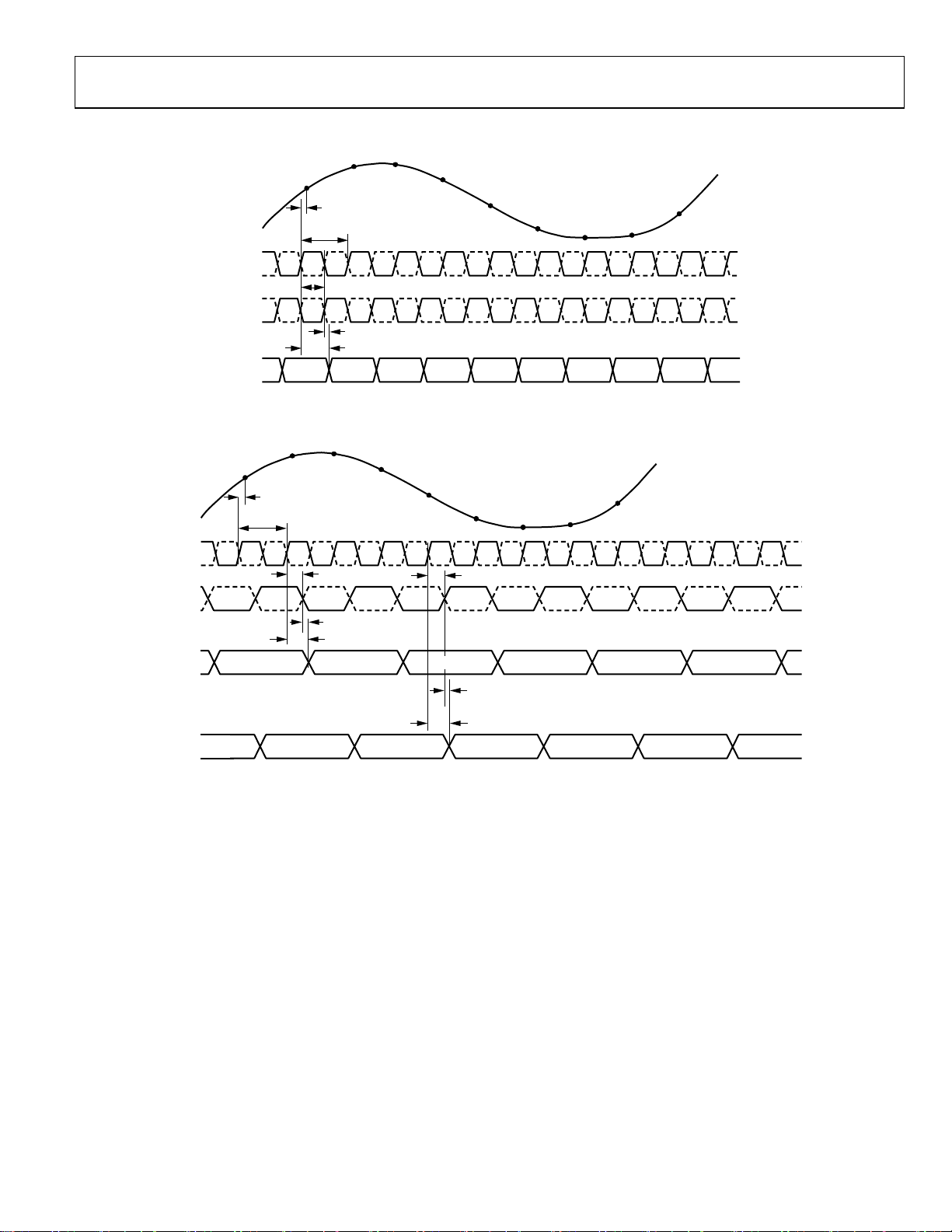
Timing Diagrams.......................................................................... 7
Absolute Maximum Ratings............................................................ 8
Thermal Resistance ...................................................................... 8
ESD Caution.................................................................................. 8
Pin Configurations and Function Descriptions ........................... 9
Equivalent Circuits......................................................................... 11
Typical Performance Characteristics ........................................... 12
Theory of Operation ...................................................................... 16
Analog Input and Voltage Reference ....................................... 16
Clock Input Considerations...................................................... 17
Power Dissipation and Power-Down Mode ........................... 18
Digital Outputs........................................................................... 18
Timing—Single Port Mode ....................................................... 19
Timing—Interleaved Mode....................................................... 19
Layout Considerations................................................................... 20
Power and Ground Recommendations................................... 20
CML ............................................................................................. 20
RBIAS........................................................................................... 20
AD9601 Configuration Using the SPI..................................... 20
Hardware Interface..................................................................... 21
Configuration Without the SPI................................................ 21
Memory Map .................................................................................. 23
Reading the Memory Map Table.............................................. 23
Reserved Locations .................................................................... 23
Default Values............................................................................. 23
Logic Levels................................................................................. 23
Evaluation Board ............................................................................ 25
Outline Dimensions ....................................................................... 31
Ordering Guide .......................................................................... 31
REVISION HISTORY
11/07—Revision 0: Initial Version
Rev. 0 | Page 2 of 32

AD9601
SPECIFICATIONS
DC SPECIFICATIONS
AVDD = 1.8 V, DRVDD = 1.8 V, T
unless otherwise noted.
Table 1.
Parameter
1
RESOLUTION 10 10 Bits
ACCURACY
No Missing Codes Full Guaranteed Guaranteed
Offset Error 25°C 4.0 4.0 mV
Full −12 +12 −12 +12 mV
Gain Error 25°C 1.4 1.4 % FS
Full −2.1 +4.5 −2.1 +4.5 % FS
Differential Nonlinearity (DNL) 25°C 0.2 0.2 LSB
Full −0.5 +0.5 −0.5 +0.5 LSB
Integral Nonlinearity (INL) 25°C 0.2 0.2 LSB
Full −0.5 +0.5 −0.5 +0.5 LSB
TEMPERATURE DRIFT
Offset Error Full 8 8 µV/°C
Gain Error Full 0.021 0.021 %/°C
ANALOG INPUTS (VIN+, VIN−)
Differential Input Voltage Range
Input Common-Mode Voltage Full 1.4 1.4 V
Input Resistance (Differential) Full 4.3 4.3 kΩ
Input Capacitance 25°C 2 2 pF
POWER SUPPLY
AVDD Full 1.7 1.8 1.9 1.7 1.8 1.9 V
DRVDD Full 1.7 1.8 1.9 1.7 1.8 1.9 V
Supply Currents
3
I
AVDD
3
I
/Single Port Mode
DRVDD
3
I
/Interleaved Mode
DRVDD
Power Dissipation
Single Port Mode
Interleaved Mode
3
4
5
4
5
Power-Down Mode Supply Currents
I
AVDD
I
DRVDD
Standby Mode Supply Currents
I
AVDD
I
DRVDD
1
See the AN-835 Application Note, Understanding High Speed ADC Testing and Evaluation, for a complete set of definitions and how these tests were completed.
2
The input range is programmable through the SPI, and the range specified reflects the nominal values of each setting. See the Memory Map section.
3
I
and I
AVDD
4
Single data rate mode; this is the default mode of the AD9601.
5
Interleaved mode; user-programmable feature. See the Memory Map section.
are measured with a −1 dBFS, 10.3 MHz sine input at rated sample rate.
DRVDD
= −40°C, T
MIN
2
= +85°C, fIN = −1.0 dBFS, full scale = 1.25 V, single port output mode, DCS enabled,
MAX
AD9601-200 AD9601-250
Temp Min Typ Max Min Typ Max Unit
Full 0.98 1.25 1.5 0.98 1.25 1.5 V p-p
Full 133 142 157 167 mA
Full 19 20 22 24 mA
Full 16 18 mA
Full mW
Full 274 291 322 344 mW
Full 268 315 mW
Full 40 40 µA
Full 170 170 22 µA
Full 19 19 mA
Full 170 170 22 µA
Rev. 0 | Page 3 of 32

AD9601
AC SPECIFICATIONS
AVDD = 1.8 V, DRVDD = 1.8 V, T
= −40°C, T
MIN
= +85°C, fIN = −1.0 dBFS, full scale = 1.25 V, DCS enabled, unless otherwise noted.
MAX
Table 2.
AD9601-200 AD9601-250
Parameter2 Temp Min Typ Max Min Typ Max Unit
SNR
fIN = 10 MHz 25°C 59.5 59.4 dB
Full 58.5 57.8 dB
fIN = 70 MHz 25°C 59.3 59.4 dB
SINAD
fIN = 10 MHz 25°C 59.5 59.4 dB
Full 58.5 57.7 dB
fIN = 70 MHz 25°C 59.3 59.4 dB
EFFECTIVE NUMBER OF BITS (ENOB)
fIN = 10 MHz 25°C 9.6 9.7 Bits
fIN = 70 MHz 25°C 9.6 9.7 Bits
WORST HARMONIC (SECOND OR THIRD)
fIN = 10 MHz 25°C 84 84 dBc
Full 77 72 dBc
fIN = 70 MHz 25°C 78 81 dBc
WORST OTHER (SFDR EXCLUDING SECOND AND THIRD)
fIN = 10 MHz 25°C 88 86 dBc
Full 80 75 dBc
fIN = 70 MHz 25°C 87 85 dBc
TWO-TONE IMD
170.2 MHz/171.3 MHz @ −7 dBFS 25°C 81 81 dBFS
ANALOG INPUT BANDWIDTH 25°C 700 700 MHz
1
All ac specifications tested by driving CLK+ and CLK− differentially.
2
See the AN-835 Application Note, Understanding High Speed ADC Testing and Evaluation, for a complete set of definitions and how these tests were completed.
1
Rev. 0 | Page 4 of 32

AD9601
DIGITAL SPECIFICATIONS
AVDD = 1.8 V, DRVDD = 1.8 V, T
Table 3.
AD9601-200 AD9601-250
Parameter1 Temp Min Typ Max Min Typ Max Unit
CLOCK INPUTS
Logic Compliance Full CMOS/LVDS/LVPECL CMOS/LVDS/LVPECL
Internal Common-Mode Bias Full 1.2 1.2 V
Differential Input Voltage Full 0.2 6 0.2 6 V p-p
Input Voltage Range Full AVDD − 0.3 AVDD + 1.6 AVDD − 0.3 AVDD + 1.6 V
Input Common-Mode Range Full 1.1 AVDD 1.1 AVDD V
High Level Input Voltage (VIH) Full 1.2 3.6 1.2 3.6 V
Low Level Input Voltage (VIL) Full 0 0.8 0 0.8 V
Input Resistance (Differential) Full 16 20 24 16 20 24 kΩ
Input Capacitance Full 4 4 pF
LOGIC INPUTS
Logic 1 Voltage Full 0.8 × VDD 0.8 × VDD V
Logic 0 Voltage Full 0.2 × AVDD 0.2 × AVDD V
Logic 1 Input Current (SDIO) Full 0 0 µA
Logic 0 Input Current (SDIO) Full −60 −60 µA
Logic 1 Input Current
(SCLK, PDWN, CSB, RESET)
Logic 0 Input Current
(SCLK, PDWN, CSB, RESET)
Input Capacitance 25°C 4 4 pF
LOGIC OUTPUTS
High Level Output Voltage Full DRVDD − 0.05 DRVDD − 0.05 V
Low Level Output Voltage Full GND + 0.05 GND + 0.05 V
Output Coding Twos complement, Gray code, or offset binary (default)
1
See the AN-835 Application Note, Understanding High Speed ADC Testing and Evaluation, for a complete set of definitions and how these tests were completed.
= −40°C, T
MIN
= +85°C, fIN = −1.0 dBFS, full scale = 1.25 V, DCS enabled, unless otherwise noted.
MAX
Full 55 50 µA
Full 0 0 µA
Rev. 0 | Page 5 of 32

AD9601
SWITCHING SPECIFICATIONS
AVDD = 1.8 V, DRVDD = 1.8 V, T
Table 4.
AD9601-200 AD9601-250
Parameter (Conditions) Temp Min Typ Max Min Typ Max Unit
Maximum Conversion Rate Full 200
Minimum Conversion Rate Full
CLK+ Pulse Width High (tCH) Full 2.15 2.4 1.8 2.0 ns
CLK+ Pulse Width Low (tCL) Full 2.15 2.4 1.8 2.0 ns
Output, Single Data Port Mode
Data Propagation Delay (tPD) 25°C 3.7 3.7 ns
DCO Propagation Delay (t
Data to DCO Skew (t
CPD
) Full 0 0.3 0.55 0 0.3 0.55 ns
SKEW
Latency Full 6 6 Cycles
SKEWA
2
PDA
CPDA
, t
SKEWB
Output, Interleaved Mode
Data Propagation Delay (t
DCO Propagation Delay (t
Data to DCO Skew (t
Latency Full 6 6 Cycles
Standby Recovery 25°C 250 250 ns
Power-Down Recovery 50 50 µs
Aperture Delay (tA) 25°C 0.1 0.1 ns
Aperture Uncertainty (Jitter, tJ) 25°C 0.2 0.2 ps rms
1
See Figure 2.
2
See Figure 3.
1
= −40°C, T
MIN
= +85°C, fIN = −1.0 dBFS, full scale = 1.25 V, DCS enabled, unless otherwise noted.
MAX
250
40
40 MSPS
MSPS
) 25°C 3.4 3.4 ns
, t
) 25°C 3.5 3.5 ns
PDB
, t
) 25°C 3.0 3.0 ns
CPDB
) Full 0 0.5 1.1 0 0.5 1.1 ns
Rev. 0 | Page 6 of 32

AD9601
TIMING DIAGRAMS
N + 2
N + 1
N
t
A
t
= 1/
f
CLK+
CLK–
DCO–
DCO+
t
DAX N – 6 N – 5 N – 4 N – 3 N – 2 N – 1 N N + 1 N + 2N – 7
CLK
t
CPD
t
SKEW
PD
N + 2
CLK+
CLK–
DCO+
DCO–
DAX
N + 1
N
t
A
t
= 1/
f
CLK
t
CPDA
t
t
PDA
SKEWA
N + 3
CLK
N – 6
N + 3
CLK
Figure 2. Single Port Mode
N + 4
N + 5
t
CPDB
N – 4
N + 4
N + 6
N + 5
N – 2
N + 7
N + 6
N + 8
N + 7
N + 8
07100-042
N
N + 2
t
SKEWB
t
PDB
DBX
N – 7
N – 5
N – 3
N – 1
N + 1
07100-043
Figure 3. Interleaved Mode
Rev. 0 | Page 7 of 32

AD9601
ABSOLUTE MAXIMUM RATINGS
Table 5.
Parameter Rating
ELECTRICAL
AVDD to AGND −0.3 V to +2.0 V
DRVDD to DRGND −0.3 V to +2.0 V
AGND to DRGND −0.3 V to +0.3 V
AVDD to DRVDD −2.0 V to +2.0 V
Dx0 Through Dx9 to DRGND −0.3 V to DRVDD + 0.3 V
DCO+/DCO− to DRGND −0.3 V to DRVDD + 0.3 V
OVRA/OVRB to DGND −0.3 V to DRVDD + 0.3 V
CLK+ to AGND −0.3 V to +3.6 V
CLK− to AGND −0.3 V to +3.6 V
VIN+ to AGND −0.3 V to AVDD + 0.2 V
VIN− to AGND −0.3 V to AVDD + 0.2 V
SDIO/DCS to DGND −0.3 V to DRVDD + 0.3 V
PDWN to AGND −0.3 V to +3.6 V
CSB to AGND −0.3 V to +3.6 V
SCLK/DFS to AGND −0.3 V to +3.6 V
ENVIRONMENTAL
Storage Temperature Range −65°C to +125°C
Operating Temperature Range −40°C to +85°C
Lead Temperature
(Soldering, 10 sec)
Junction Temperature 150°C
300°C
Stresses above those listed under Absolute Maximum Ratings
may cause permanent damage to the device. This is a stress
rating only; functional operation of the device at these or any
other conditions above those indicated in the operational
section of this specification is not implied. Exposure to absolute
maximum rating conditions for extended periods may affect
device reliability.
THERMAL RESISTANCE
The exposed paddle must be soldered to the ground plane for
the LFCSP package. Soldering the exposed paddle to the
customer board increases the reliability of the solder joints,
maximizing the thermal capability of the package.
Table 6.
Package Type θ
56-Lead LFCSP (CP-56-2) 30.4 2.9 °C/W
JA
θ
JC
Unit
Typical θJA and θJC are specified for a 4-layer board in still air.
Airflow increases heat dissipation, effectively reducing θ
JA
. In
addition, metal in direct contact with the package leads from
metal traces, and through holes, ground, and power planes
reduces the θ
.
JA
ESD CAUTION
Rev. 0 | Page 8 of 32

AD9601
PIN CONFIGURATIONS AND FUNCTION DESCRIPTIONS
A1
D
DA0 (LSB)
NIC
DA2
54
53
55
PIN 1
INDICATO R
17
16
18
B6
D
DB5
DB4
NIC
52
51
AD9601
TOP VIEW
(Not to Scale)
20
19
DB8
DB7
DA3
56
1DA4
2DA5
3DA6
4DA7
5DA8
6(MSB) DA9
7DRVDD
8DRGND
9OVRA
10NIC
11NIC
12(L SB) DB0
PIN 0 (EXPOSED PADDLE) = AGND
13DB1
14DB2
15
DB3
DCO+
DCO–
DRGND
50
49
48
21
23
22
OVRB
RGND
D
(MSB) DB9
VDD
A
CLK+
DRVDD
AVDD
CLK–
43
44
47
46
45
42 AVDD
41 AVDD
40 CML
39 AVDD
38 AVDD
37 AVDD
36 VIN–
35 VIN+
34 AVDD
33 AVDD
32 AVDD
31 RBIAS
30 AVDD
29 PWDN
28
27
25
26
24
ET
CSB
RES
DRVDD
SDIO/DCS
SCLK/DFS
07100-002
Figure 4. Pin Configuration
Table 7. Single Data Rate Mode Pin Function Descriptions
Pin No. Mnemonic Description
30, 32, 33, 34, 37, 38, 39,
AVDD 1.8 V Analog Supply.
41, 42, 43, 46
7, 24, 47 DRVDD 1.8 V Digital Output Supply.
0 AGND
8, 23, 48 DRGND
1
1
Analog Ground.
Digital Output Ground.
35 VIN+ Analog Input—True.
36 VIN− Analog Input—Complement.
40 CML
Common-Mode Output Pin. Enabled through the SPI, this pin provides a reference for the
optimized internal bias voltage for VIN+/VIN−.
44 CLK+ Clock Input—True.
45 CLK− Clock Input—Complement.
31 RBIAS
Set Pin for Chip Bias Current. (Place 1% 10 kΩ resistor terminated to ground.)
Nominally 0.5 V.
28 RESET CMOS-Compatible Chip Reset (Active Low).
25 SDIO/DCS
Serial Port Interface (SPI) Data Input/Output (Serial Port Mode); Duty Cycle Stabilizer
Select (External Pin Mode).
26 SCLK/DFS Serial Port Interface Clock (Serial Port Mode); Data Format Select Pin (External Pin Mode).
27 CSB Serial Port Chip Select (Active Low).
29 PWDN Chip Power-Down.
49 DCO− Data Clock Output—Complement.
50 DCO+ Data Clock Output—True.
53 DA0 (LSB) Output Port A Output Bit 0 (LSB).
54 DA1 Output Port A Output Bit 1.
55 DA2 Output Port A Output Bit 2.
56 DA3 Output Port A Output Bit 3.
1 DA4 Output Port A Output Bit 4.
2 DA5 Output Port A Output Bit 5.
3 DA6 Output Port A Output Bit 6.
Rev. 0 | Page 9 of 32

AD9601
Pin No. Mnemonic Description
4 DA7 Output Port A Output Bit 7.
5 DA8 Output Port A Output Bit 8.
6 DA9 (MSB) Output Port A Output Bit 9 (MSB).
10, 11, 51, 52 NIC Not internally connected.
9 OVRA Output Port A Overrange Output Bit.
12 DB0 (LSB) Output Port B Output Bit 0 (LSB).
13 DB1 Output Port B Output Bit 1.
14 DB2 Output Port B Output Bit 2.
15 DB3 Output Port B Output Bit 3.
16 DB4 Output Port B Output Bit 4.
17 DB5 Output Port B Output Bit 5.
18 DB6 Output Port B Output Bit 6.
19 DB7 Output Port B Output Bit 7.
20 DB8 Output Port B Output Bit 8.
21 DB9 (MSB) Output Port B Output Bit 9 (MSB).
22 OVRB Output Port B Overrange Output Bit.
1
AGND and DRGND should be tied to a common quiet ground plane.
Rev. 0 | Page 10 of 32
 Loading...