ANALOG DEVICES AD9575 Service Manual

V
Network Clock Generator, Two Outputs
FEATURES
Fully integrated VCO/PLL core
0.39 ps rms jitter from 12 kHz to 20 MHz at 156.25 MHz
0.15 ps rms jitter from 1.875 MHz to 20 MHz at 156.25 MHz
0.40 ps rms jitter from 12 kHz to 20 MHz at 106.25 MHz
0.15 ps rms jitter from 637 kHz to 10 MHz at 106.25 MHz
Input crystal frequency of 19.44 MHz, 25 MHz, or
25.78125 MHz
Pin selectable divide ratios for 33.33 MHz, 62.5 MHz,
100 MHz, 106.25 MHz, 125 MHz, 155.52 MHz, 156.25 MHz,
159.375 MHz, 161.13 MHz, and 312.5 MHz outputs
LVDS/LVPECL/LVCMOS output format
Integrated loop filter
Space saving 4.4 mm × 5.0 mm TSSOP
100 mA power supply current (LVDS output)
120 mA power supply current (LVPECL output)
3.3 V operation
APPLICATIONS
GbE/FC/SONET line cards, switches, and routers
CPU/PCI-E applications
Low jitter, low phase noise clock generation
AD9575
GENERAL DESCRIPTION
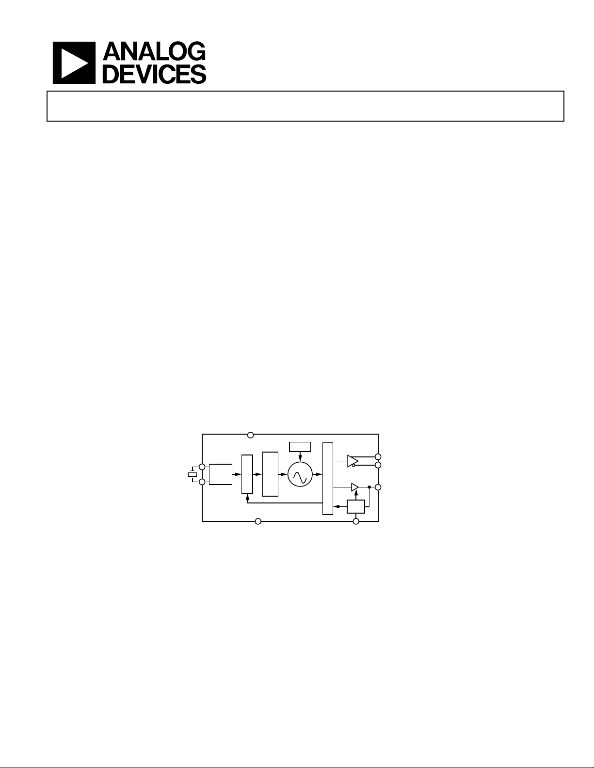
The AD9575 provides a highly integrated, dual output clock
generator function including an on-chip PLL core that is
optimized for network clocking. The integer-N PLL design is
based on the Analog Devices, Inc., proven portfolio of high
performance, low jitter frequency synthesizers to maximize line
card performance. Other applications with demanding phase
noise and jitter requirements also benefit from this part.
The PLL section consists of a low noise phase frequency detector
(PFD), a precision charge pump (CP), a low phase noise voltage
controlled oscillator (VCO), and pin selectable feedback and
output dividers.
By connecting an external crystal, popular network output frequencies can be locked to the input reference. The output divider
and feedback divider ratios are pin programmable for the required
output rates. No external loop filter components are required,
thus conserving valuable design time and board space.
The AD9575 is available in a 16-lead, 4.4 mm × 5.0 mm TSSOP
and can be operated from a single 3.3 V supply. The temperature
range is −40°C to +85°C.
FUNCTIONAL BLOCK DIAGRAM
DD × 5
XTAL
OSC
AD9575
GND × 5
Rev. A
Rev. A
Information furnished by Analog Devices is believed to be accurate and reliable. However, no
Information furnished by Analog Devices is believed to be accurate and reliable. However, no
responsibility is assumed by Analog Devices for its use, nor for any infringements of patents or other
responsibility is assumed by Analog Devices for its use, nor for any infringements of patents or other
rights of third parties that may result from its use. Specifications subject to change without notice. No
rights of third parties that may result from its use. Specifications subject to change without notice. No
license is granted by implication or otherwise under any patent or patent rights of Analog Devices.
license is granted by implication or otherwise under any patent or patent rights of Analog Devices.
Trademarks and registered trademarks are the property of their respective owners.
Trademarks and registered trademarks are the property of their respective owners.
LPF
PFD/CP
THIRD-ORDER
LDO
VCO
Figure 1.
LVDS OR
LVPECL
LVCMOS
DIVIDERS
SEL
SEL0
One Technology Way, P.O. Box 9106, Norwood, MA 02062-9106, U.S.A.
One Technology Way, P.O. Box 9106, Norwood, MA 02062-9106, U.S.A.
Tel: 781.329.4700 www.analog.com
Tel: 781.329.4700 www.analog.com
Fax: 781.461.3113 ©2010 Analog Devices, Inc. All rights reserved.
Fax: 781.461.3113 ©2010 Analog Devices, Inc. All rights reserved.
100MHz
TO 312.5M Hz
33.33MHz/
62.5MHz/SEL1
08462-001

AD9575
TABLE OF CONTENTS
Features .............................................................................................. 1
Applications ....................................................................................... 1
General Description ......................................................................... 1
Functional Block Diagram .............................................................. 1
Revision History ............................................................................... 2
Specifications ..................................................................................... 3
PLL Characteristics ...................................................................... 3
LVDS Clock Output Jitter (Typ/Max) ........................................ 4
LVPECL Clock Output Jitter (Typ/Max) ................................... 4
Output Frequency Select ............................................................. 5
Clock Outputs ............................................................................... 5
Timing Characteristics ................................................................ 5
Power .............................................................................................. 6
Crystal Oscillator .......................................................................... 6
Timing Diagrams .......................................................................... 6
Absolute Maximum Ratings ............................................................7
Thermal Resistance .......................................................................7
ESD Caution...................................................................................7
Pin Configuration and Function Descriptions ..............................8
Typical Performance Characteristics ..............................................9
Terminolog y .................................................................................... 11
Theory of Operation ...................................................................... 12
Phase Frequency Detector (PFD) and Charge Pump ............ 12
Power Supply ............................................................................... 12
LVPECL Clock Distribution ..................................................... 12
LVDS Clock Distribution .......................................................... 13
LVCMOS Clock Distribution ................................................... 13
Typical Application Circuit ....................................................... 13
Outline Dimensions ....................................................................... 14
Ordering Guide .......................................................................... 14
REVISION HISTORY
3/10—Rev. 0 to Rev. A
Changes to Features Section............................................................ 1
Changes to Table 1, Table 2, and Table 3 ....................................... 4
Changes to Table 4 and Table 6 ....................................................... 5
Changes to Table 7 and Table 8 ....................................................... 6
Changes to Table 12 .......................................................................... 8
Added Figure 11; Renumbered Figures Sequentially ................ 10
Changes to Figure 13 ...................................................................... 10
Changes to Theory of Operation Section and Figure 19 ........... 12
Changes to Figure 24 ...................................................................... 13
1/10—Revision 0: Initial Version
Rev. A | Page 2 of 16

AD9575
SPECIFICATIONS
Typical (typ) values are given for VS = 3.3 V ± 10%, TA = 25°C, unless otherwise noted. Minimum (min) and maximum (max) values are
given over the full V
PLL CHARACTERISTICS
Table 1.
LVD S LVC MOS LVP ECL
Parameter Min Typ Max Min Typ Max Min Typ Max Unit
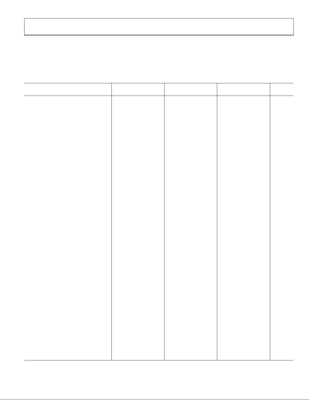
PHASE NOISE CHARACTERISTICS
PLL Noise (100 MHz Output)
At 1 kHz −123 −122 dBc/Hz
At 10 kHz −128 −129 dBc/Hz
At 100 kHz −131 −131 dBc/Hz
At 1 MHz −150 −151 dBc/Hz
At 10 MHz −156 −158 dBc/Hz
At 30 MHz −156 −158 dBc/Hz
PLL Noise (106.25 MHz Output)
At 1 kHz −121 −121 dBc/Hz
At 10 kHz −127 −128 dBc/Hz
At 100 kHz −130 −130 dBc/Hz
At 1 MHz −149 −150 dBc/Hz
At 10 MHz −156 −158 dBc/Hz
At 30 MHz −156 −159 dBc/Hz
PLL Noise (125 MHz Output)
At 1 kHz −120 −120 dBc/Hz
At 10 kHz −126 −127 dBc/Hz
At 100 kHz −128 −129 dBc/Hz
At 1 MHz −148 −150 dBc/Hz
At 10 MHz −155 −157 dBc/Hz
At 30 MHz −156 −158 dBc/Hz
PLL Noise (155.52 MHz Output)
At 1 kHz −118 −118 dBc/Hz
At 10 kHz −123 −123 dBc/Hz
At 100 kHz −125 −125 dBc/Hz
At 1 MHz −147 −149 dBc/Hz
At 10 MHz −155 −157 dBc/Hz
At 30 MHz −156 −157 dBc/Hz
PLL Noise (156.25 MHz Output)
At 1 kHz −118 −118 dBc/Hz
At 10 kHz −124 −125 dBc/Hz
At 100 kHz −126 −127 dBc/Hz
At 1 MHz −146 −148 dBc/Hz
At 10 MHz −155 −157 dBc/Hz
At 30 MHz −155 −157 dBc/Hz
PLL Noise (159.375 MHz Output)
At 1 kHz −118 −118 dBc/Hz
At 10 kHz −124 −125 dBc/Hz
At 100 kHz −126 −126 dBc/Hz
At 1 MHz −146 −147 dBc/Hz
At 10 MHz −155 −156 dBc/Hz
At 30 MHz −155 −157 dBc/Hz
and TA (−40°C to +85°C) variation.
S
Rev. A | Page 3 of 16

AD9575
LVD S LVC MOS LVP ECL
Parameter Min Typ Max Min Typ Max Min Typ Max Unit
PLL Noise (161.132812 MHz Output)
At 1 kHz −118 −119 dBc/Hz
At 10 kHz −122 −123 dBc/Hz
At 100 kHz −126 −126 dBc/Hz
At 1 MHz −144 −146 dBc/Hz
At 10 MHz −154 −156 dBc/Hz
At 30 MHz −155 −156 dBc/Hz
PLL Noise (312.5 MHz Output)
At 1 kHz −112 −112 dBc/Hz
At 10 kHz −119 −119 dBc/Hz
At 100 kHz −120 −120 dBc/Hz
At 1 MHz −140 −142 dBc/Hz
At 10 MHz −152 −154 dBc/Hz
At 30 MHz −153 −155 dBc/Hz
PLL Noise (33.33 MHz Output)
At 1 kHz −131 dBc/Hz
At 10 kHz −138 dBc/Hz
At 100 kHz −140 dBc/Hz
At 1 MHz −155 dBc/Hz
At 5 MHz −155 dBc/Hz
PLL Noise (62.5 MHz Output)
At 1 kHz −126 dBc/Hz
At 10 kHz −133 dBc/Hz
At 100 kHz −134 dBc/Hz
At 1 MHz −150 dBc/Hz
At 5 MHz −152 dBc/Hz
Spurious Content −70 −70 dBc
PLL Figure of Merit −217 −217 dBc/Hz
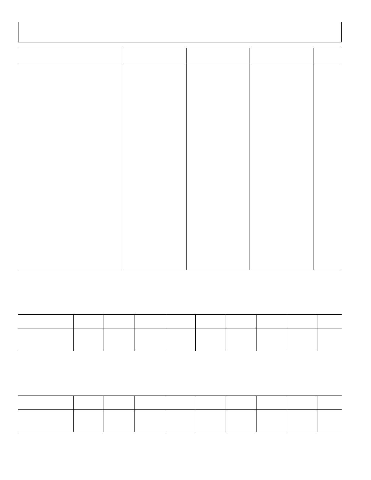
LVDS CLOCK OUTPUT JITTER (TYP/MAX)
Typical (typ) values are given for VS = 3.3 V ± 10%, TA = 25°C, unless otherwise noted. Maximum (max) values are given over the full VS
and T
(−40°C to +85°C) variation.
A
Table 2.
Jitter Integration
Bandwidth
12 kHz to 20 MHz 0.38/0.50 0.40/0.54 0.37/0.47 0.41/0.54 0.39/0.51 0.38/0.51 0.44/0.61 0.36/0.48 ps rms
1.875 MHz to 20 MHz 0.15/0.27 ps rms
637 kHz to 10 MHz 0.15/0.21 ps rms
100
MHz
106.25
MHz
125
MHz
155.52
MHz
156.25
MHz
159.375
MHz
161.13
MHz
312.5
MHz Unit
LVPECL CLOCK OUTPUT JITTER (TYP/MAX)
Typical (typ) values are given for VS = 3.3 V ± 10%, TA = 25°C, unless otherwise noted. Maximum (max) values are given over the full VS
and T
(−40°C to +85°C) variation.
A
Table 3.
Jitter Integration
Bandwidth
12 kHz to 20 MHz 0.36/0.46 0.44/0.68 0.36/0.45 0.40/0.52 0.39/0.64 0.41/0.62 0.43/0.69 0.38/0.49 ps rms
1.875 MHz to 20 MHz 0.19/0.54 ps rms
637 kHz to 10 MHz 0.22/0.35 ps rms
100
MHz
106.25
MHz
125
MHz
155.52
MHz
Rev. A | Page 4 of 16
156.25
MHz
159.375
MHz
161.13
MHz
312.5
MHz
Unit

AD9575
OUTPUT FREQUENCY SELECT
Minimum (min) and maximum (max) values are given over the full VS and TA (−40°C to +85°C) variation.
Table 4.
Parameter Min Typ Max Unit Test Conditions/Comments
Select Pins (SEL0/SEL1)
Logic 1 Voltage 0.83 × VS + 0.2 V
Logic 0 Voltage 0.33 × VS − 0.2 V
Logic 1 Current 190 μA Pull-up to VS
Logic 0 Current 150 μA Pull-down to GND
CLOCK OUTPUTS
Typical (typ) values are given for VS = 3.3 V ± 10%, TA = 25°C, unless otherwise noted. Minimum (min) and maximum (max) values are
given over the full V
Table 5.
Parameter Min Typ Max Unit Test Conditions/Comments
LVDS CLOCK OUTPUT Termination = 100 Ω differential; default
Output Frequency 312.5 MHz
Differential Output Voltage (VOD) 250 340 450 mV See Figure 2 for definition
Delta VOD 25 mV
Output Offset Voltage (VOS) 1.125 1.25 1.375 V
Delta VOS 25 mV
Short-Circuit Current (ISA, ISB) 14 24 mA Output shorted to GND
Duty Cycle 45 50 55 %
LVPECL CLOCK OUTPUT
Output Frequency 312.5 MHz
Output High Voltage (VOH) VS − 1.5 VS − 1.05 VS − 0.8 V
Output Low Voltage (VOL) VS − 2.5 VS − 1.75 VS − 1.7 V
Differential Output Voltage (VOD) 430 640 800 mV See Figure 2 for definition
Duty Cycle 45 50 55 %
LVCMOS CLOCK OUTPUT
Output Frequency 62.5 MHz
Output High Voltage (VOH) VS − 0.1 V
Output Low Voltage (VOL) 0.1 V
Duty Cycle 45 50 55 %
and TA (−40°C to +85°C) variation.
S
TIMING CHARACTERISTICS
Table 6.
Parameter Min Typ Max Unit Test Conditions/Comments
LVDS
Termination = 100 Ω differential; C
= 0.1 μF
C
AC
Output Rise Time, tRL 150 200 300 ps 20% to 80%, measured differentially
Output Fall Time, tFL 150 200 300 ps 80% to 20%, measured differentially
LVPECL
Termination = 200 Ω to GND; C
= 0.1 μF
C
AC
Output Rise Time, tRL 180 250 300 ps 20% to 80%, measured differentially
Output Fall Time, tFL 180 250 300 ps 80% to 20%, measured differentially
LVCMOS
Termination = 50 Ω to 0 V; C
= 0.1 μF
C
AC
LOAD
Output Rise Time, tRC 0.50 0.70 1.10 ns 20% to 80%
Output Fall Time, tFC 0.50 0.70 1.10 ns 80% to 20%
Rev. A | Page 5 of 16
LOAD
= 0 pF;
LOAD
= 5 pF;
= 0 pF;
 Loading...