Fiber Channel/Ethernet Clock Generator IC,
FEATURES
Fully integrated dual VCO/PLL cores
0.22 ps rms jitter from 0.637 MHz to 10 MHz at 106.25 MHz
0.19 ps rms jitter from 1.875 MHz to 20 MHz at 156.25 MHz
0.42 ps rms jitter from 12 kHz to 20 MHz at 125 MHz
Input crystal or clock frequency of 25 MHz
Preset divide ratios for 106.25 MHz, 156.25 MHz, 33.33 MHz,
100 MHz, and 125 MHz
Choice of LVPECL or LVDS output format
Integrated loop filters
Copy of reference clock output
Rates configured via strapping pins
0.71 W power dissipation (LVDS operation)
1.07 W power dissipation (LVPECL operation)
3.3 V operation
Space saving, 6 mm × 6 mm, 40-lead LFCSP
APPLICATIONS
Fiber channel line cards, switches, and routers
Gigabit Ethernet/PCIe support included
Low jitter, low phase noise clock generation
GENERAL DESCRIPTION
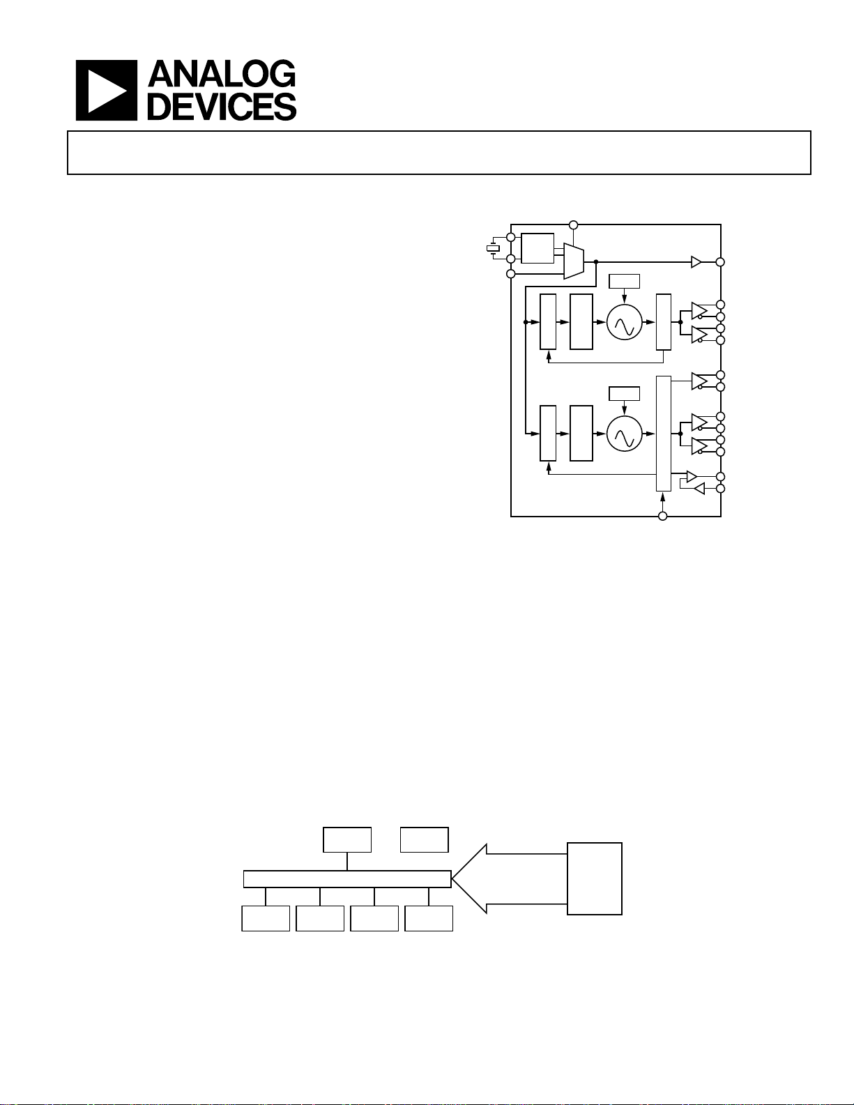
The AD9572 provides a multioutput clock generator function
along with two on-chip PLL cores, optimized for fiber channel
line card applications that include an Ethernet interface. The
integer-N PLL design is based on the Analog Devices, Inc.,
proven portfolio of high performance, low jitter frequency
synthesizers to maximize network performance. Other applications with demanding phase noise and jitter requirements also
benefit from this part.
The PLL section consists of a low noise phase frequency
detector (PFD), a precision charge pump (CP), a low phase
noise voltage controlled oscillator (VCO), and a preprogrammed
7 Clock Outputs
AD9572
FUNCTIONAL BLOCK DIAGRAM
REFSEL
XTAL
OSC
REFCLK
PFD/CP
PFD/CP
AD9572
LDO
VCO
ORDER
LPF THIRD
LDO
VCO
LPF
3RD ORDER
Figure 1.
feedback divider and output divider. By connecting an external
crystal or reference clock to the REFCLK pin, frequencies up to
156.25 MHz can be locked to the input reference. Each output
divider and feedback divider ratio is preprogrammed for the
required output rates.
A second PLL also operates as an integer-N synthesizer and
drives two LVPECL or LVDS output buffers for 106.25 MHz
operation. No external loop filter components are required, thus
conserving valuable design time and board space.
The AD9572 is available in a 40-lead, 6 mm × 6 mm lead frame
chip scale package (LFCSP) and can be operated from a single
3.3 V supply. The temperature range is −40°C to +85°C.
DIVIDE RS
DIVIDERS
FREQSEL
CMOS
LVPECL
OR LVDS
LVPECL
OR LVDS
LVPECL
OR LVDS
CMOS
1 × 25MHz
2 × 106.25MHz
1 × 156.25MHz
2 × 100MHz
OR 125MHz
1 × 33.33MHz
FORCE_LO W
7498-001
16-PORT FIBRE CHANNEL ASIC
QUAD SFP
PHY
QUAD SFP
PHY
10G SFP+
QUAD SFP
PHY
ISLAND
QUAD SFP
Figure 2. Typical Application
Rev. B
Information furnished by Analog Devices is believed to be accurate and reliable. However, no
responsibility is assumed by Anal og Devices for its use, nor for any infringements of patents or ot her
rights of third parties that may result from its use. Specifications subject to change without notice. No
license is granted by implication or otherwise under any patent or patent rights of Analog Devices.
Trademarks and registered trademarks are the property of their respective owners.
CPU
PHY
1 × 156.25MHz
2 × 106.25MHz
1 × 100MHz/125MHz
1 × 25MHz
1 × 33.33MHz
One Technology Way, P.O. Box 9106, Norwood, MA 02062-9106, U.S.A.
Tel: 781.329.4700 www.analog.com
Fax: 781.461.3113 ©2009-2011 Analog Devices, Inc. All rights reserved.
AD9572
7498-002

AD9572
TABLE OF CONTENTS
Features.............................................................................................. 1
Applications....................................................................................... 1
Functional Block Diagram .............................................................. 1
General Description ......................................................................... 1
Revision History ............................................................................... 2
Specifications..................................................................................... 3
PLL Characteristics ...................................................................... 3
LVDS Clock Output Jitter............................................................ 4
LVPECL Clock Output Jitter....................................................... 5
CMOS Clock Output Jitter.......................................................... 5
Reference Input............................................................................. 5
Clock Outputs............................................................................... 6
Timing Characteristics ................................................................ 6
Control Pins .................................................................................. 7
Power.............................................................................................. 7
Crystal Oscillator.......................................................................... 7
Timing Diagrams.............................................................................. 8
Absolute Maximum Ratings............................................................ 9
Thermal Resistance ...................................................................... 9
ESD Caution...................................................................................9
Pin Configuration and Function Descriptions........................... 10
Typical Performance Characteristics........................................... 13
Terminology.................................................................................... 15
Theory of Operation ...................................................................... 16
Outputs........................................................................................ 16
Phase Frequency Detector (PFD) and Charge Pump............ 17
Power Supply............................................................................... 17
CMOS Clock Distribution ........................................................ 17
LVPECL Clock Distribution..................................................... 18
LVDS Clock Distribution.......................................................... 18
Reference Input........................................................................... 18
Power and Grounding Considerations and Power Supply
Rejection...................................................................................... 19
Outline Dimensions....................................................................... 20
Ordering Guide .......................................................................... 20
REVISION HISTORY
/11—Rev. A to Rev. B
C
hanges to Output Rise Time, t
Time, t
11/10—Rev. 0 to Rev. A
Changes to Features.......................................................................... 1
Changes to Table 2............................................................................ 4
Changes to Table 3 and Table 4....................................................... 5
Changes to Table 7............................................................................ 6
Added Figure 7 and Figure 8......................................................... 11
Added Figure 14, Figure 15, and Figure 16................................. 13
Deleted Original Figure 16 and Figure 19................................... 16
Parameter in Table 7....................................................... 6
FC2
Parameter and Output Fall
RC2
Renumbered Figures Sequentially............................... Throughout
Changes to CMOS Clock Distribution Section.......................... 17
Changes to LVPECL Clock Distribution Section, Added
Figure 23 and Figure 24................................................................. 18
Changes to LVDS Clock Distribution Section, Added
Figure 26 .......................................................................................... 18
Changes to Reference Input Section ............................................ 18
Changes to Power and Grounding Considerations and Power
Supply Rejection Section ............................................................... 19
7/09—Revision 0: Initial Version
Rev. B | Page 2 of 20

AD9572
SPECIFICATIONS
PLL CHARACTERISTICS
Typical (typ) is given for VS = 3.3 V, TA = 25°C, unless otherwise noted.
Table 1.
Parameter Min Typ Max Unit Test Conditions/Comments
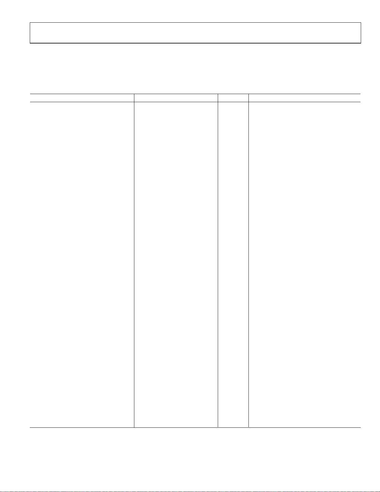
PHASE NOISE CHARACTERISTICS
PLL Noise (106.25 MHz LVDS Output)
At 1 kHz −123 dBc/Hz 33.33 MHz output disabled
At 10 kHz −127 dBc/Hz 33.33 MHz output disabled
At 100 kHz −129 dBc/Hz 33.33 MHz output disabled
At 1 MHz −150 dBc/Hz 33.33 MHz output disabled
At 10 MHz −152 dBc/Hz 33.33 MHz output disabled
At 30 MHz −153 dBc/Hz 33.33 MHz output disabled
PLL Noise (156.25 MHz LVDS Output)
At 1 kHz −118 dBc/Hz 33.33 MHz output disabled
At 10 kHz −125 dBc/Hz 33.33 MHz output disabled
At 100 kHz −126 dBc/Hz 33.33 MHz output disabled
At 1 MHz −145 dBc/Hz 33.33 MHz output disabled
At 10 MHz −151 dBc/Hz 33.33 MHz output disabled
At 30 MHz −151 dBc/Hz 33.33 MHz output disabled
PLL Noise (125 MHz LVDS Output)
At 1 kHz −119 dBc/Hz 33.33 MHz output disabled
At 10 kHz −127 dBc/Hz 33.33 MHz output disabled
At 100 kHz −128 dBc/Hz 33.33 MHz output disabled
At 1 MHz −147 dBc/Hz 33.33 MHz output disabled
At 10 MHz −151 dBc/Hz 33.33 MHz output disabled
At 30 MHz −152 dBc/Hz 33.33 MHz output disabled
PLL Noise (100 MHz LVDS Output)
At 1 kHz −121 dBc/Hz 33.33 MHz output disabled
At 10 kHz −128 dBc/Hz 33.33 MHz output disabled
At 100 kHz −130 dBc/Hz 33.33 MHz output disabled
At 1 MHz −147 dBc/Hz 33.33 MHz output disabled
At 10 MHz −150 dBc/Hz 33.33 MHz output disabled
At 30 MHz −150 dBc/Hz 33.33 MHz output disabled
PLL Noise (106.25 MHz LVPECL Output)
At 1 kHz −121 dBc/Hz 33.33 MHz output disabled
At 10 kHz −128 dBc/Hz 33.33 MHz output disabled
At 100 kHz −129 dBc/Hz 33.33 MHz output disabled
At 1 MHz −151 dBc/Hz 33.33 MHz output disabled
At 10 MHz −154 dBc/Hz 33.33 MHz output disabled
At 30 MHz −155 dBc/Hz 33.33 MHz output disabled
PLL Noise (156.25 MHz LVPECL Output)
At 1 kHz −119 dBc/Hz 33.33 MHz output disabled
At 10 kHz −125 dBc/Hz 33.33 MHz output disabled
At 100 kHz −126 dBc/Hz 33.33 MHz output disabled
At 1 MHz −147 dBc/Hz 33.33 MHz output disabled
At 10 MHz −152 dBc/Hz 33.33 MHz output disabled
At 30 MHz −153 dBc/Hz 33.33 MHz output disabled
Rev. B | Page 3 of 20

AD9572
Parameter Min Typ Max Unit Test Conditions/Comments
PLL Noise (125 MHz LVPECL Output)
At 1 kHz −122 dBc/Hz 33.33 MHz output disabled
At 10 kHz −127 dBc/Hz 33.33 MHz output disabled
At 100 kHz −128 dBc/Hz 33.33 MHz output disabled
At 1 MHz −148 dBc/Hz 33.33 MHz output disabled
At 10 MHz −152 dBc/Hz 33.33 MHz output disabled
At 30 MHz −153 dBc/Hz 33.33 MHz output disabled
PLL Noise (100 MHz LVPECL Output)
At 1 kHz −122 dBc/Hz 33.33 MHz output disabled
At 10 kHz −128 dBc/Hz 33.33 MHz output disabled
At 100 kHz −130 dBc/Hz 33.33 MHz output disabled
At 1 MHz −148 dBc/Hz 33.33 MHz output disabled
At 10 MHz −150 dBc/Hz 33.33 MHz output disabled
At 30 MHz −151 dBc/Hz 33.33 MHz output disabled
PLL Noise (33.33 MHz CMOS Output)
At 1 kHz −130 dBc/Hz
At 10 kHz −138 dBc/Hz
At 100 kHz −139 dBc/Hz
At 1 MHz −152 dBc/Hz
At 5 MHz −152 dBc/Hz
Phase Noise (25 MHz CMOS Output)
At 1 kHz −133 dBc/Hz
At 10 kHz −142 dBc/Hz
At 100 kHz −148 dBc/Hz
At 1 MHz −148 dBc/Hz
At 5 MHz −148 dBc/Hz
Spurious Content1 −70 dBc Dominant amplitude, all outputs active
PLL Figure of Merit −217.5 dBc/Hz
1
When the 33.33 MHz, 100 MHz, and 125 MHz clocks are enabled simultaneously, a worst-case −50 dBc spurious content might be presented on Pin 21 and Pin 22 only.
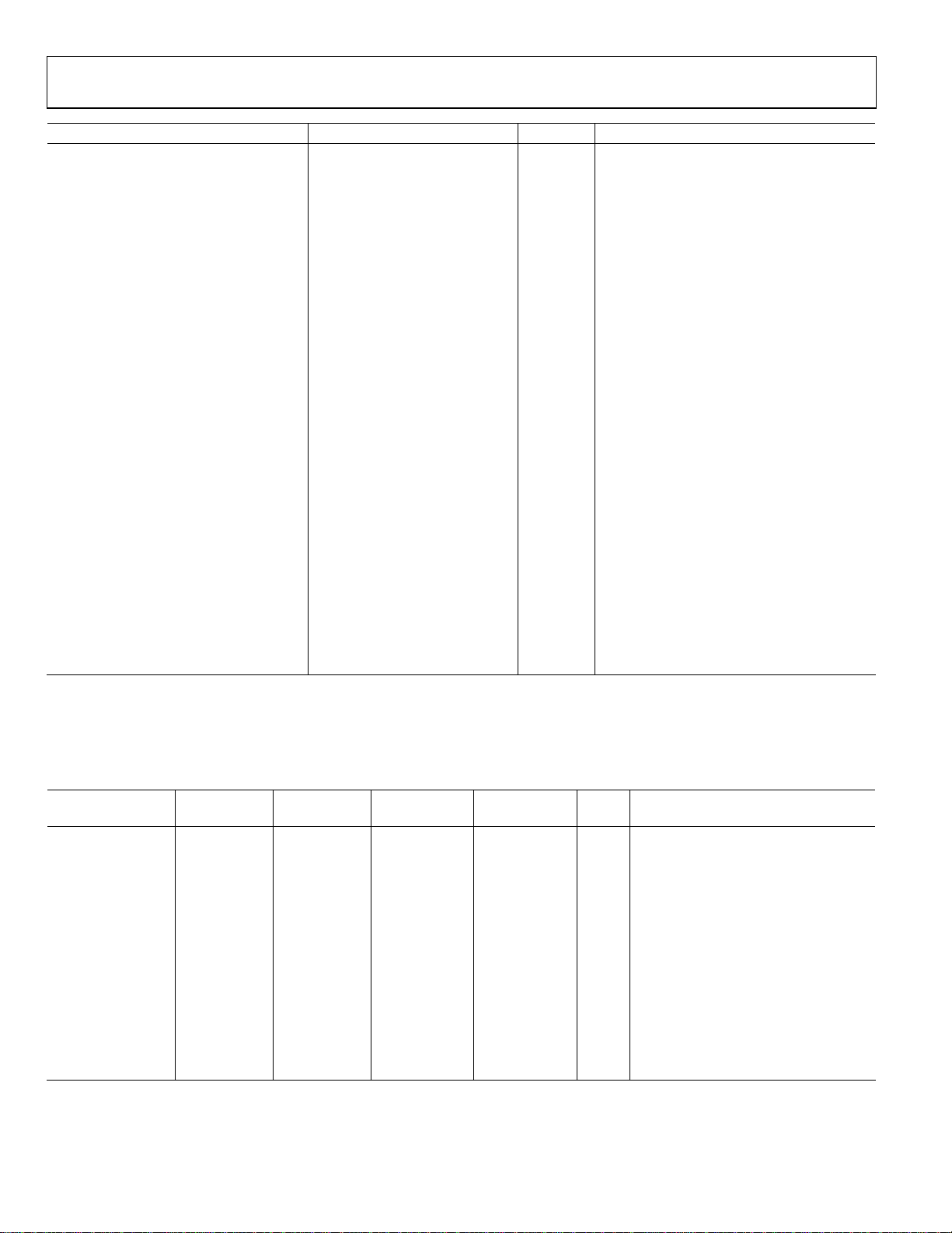
LVDS CLOCK OUTPUT JITTER
Typical (typ) is given for VS = 3.3 V, TA = 25°C, unless otherwise noted.
Table 2.
Jitter Integration
Bandwidth (Typ) 100 MHz 106.25 MHz
12 kHz to 20 MHz 0.51 0.44 0.42/0.88 0.42
1.875 MHz to
0.19
20 MHz
637 kHz to 10 MHz 0.22
200 kHz to 10 MHz 0.32 0.25/0.78
12 kHz to 35 MHz 0.50 (off only)
1
The typical 125 MHz rms jitter data is collected from the differential pair, Pin 21 and Pin 22, unless otherwise noted.
125 MHz 33M
= Off/On
1
156.25 MHz Unit Test Conditions/Comments
Rev. B | Page 4 of 20
ps
rms
ps
rms
ps
rms
ps
rms
ps
rms
LVDS output frequency combinations
are 1 × 156.25 MHz, 1 × 100 MHz, 1 ×
125 MHz, 2 × 106.25 MHz
LVDS output frequency combinations
are 1 × 156.25 MHz, 1 × 100 MHz, 1 ×
125 MHz, 2 × 106.25 MHz
LVDS output frequency combinations
are 1 × 156.25 MHz, 1 × 100 MHz, 1 ×
125 MHz, 2 × 106.25 MHz
LVDS output frequency combinations
are 1 × 156.25 MHz, 1 × 100 MHz, 1 ×
125 MHz, 2 × 106.25 MHz
LVDS output frequency combinations
are 1 × 156.25 MHz, 2 × 125 MHz, 2 ×
106.25 MHz

AD9572
LVPECL CLOCK OUTPUT JITTER
Typical (typ) is given for VS = 3.3 V, TA = 25°C, unless otherwise noted.
Table 3.
125 MHz
Jitter Integration
Bandwidth (Typ)
12 kHz to 20 MHz (Typ) 0.61 0.45 0.44/2.2 0.46 ps rms
12 kHz to 20 MHz (Max) 0.87 0.81
1.875 MHz to 20 MHz (Typ) 0.28 ps rms
637 kHz to 10 MHz (Typ) 0.23 ps rms
200 kHz to 10 MHz (Typ) 0.38 0.24/2.2 ps rms
12 kHz to 35 MHz (Typ)
12 kHz to 35 MHz (Max)
CMOS CLOCK OUTPUT JITTER
Typical (typ) is given for VS = 3.3 V, TA = 25°C, unless otherwise noted.
100
MHz
106.25
MHz
33M =
Off/On
0.56 (off
only)
0.52 (off
only)
0.66 (off
only)
156.25
MHz Unit Test Conditions/Comments
LVPECL output frequency combinations are 1 × 156.25
MHz, 1 × 100 MHz, 1 × 125 MHz, 2 × 106.25 MHz
0.56 ps rms
ps rms
ps rms
LVPECL output frequency combinations are 1 × 156.25
MHz, 1 × 100 MHz, 1 × 125 MHz, 2 × 106.25 MHz
LVPECL output frequency combinations are 1 × 156.25
MHz, 1 × 100 MHz, 1 × 125 MHz, 2 × 106.25 MHz
LVPECL output frequency combinations are 1 × 156.25
MHz, 1 × 100 MHz, 1 × 125 MHz, 2 × 106.25 MHz
LVPECL output frequency combinations are 1 × 156.25
MHz, 1 × 100 MHz, 1 × 125 MHz, 2 × 106.25 MHz
LVPECL output frequency combinations are 156.25
MHz unterminated, 2 × 125 MHz, 2 × 106.25 MHz
LVPECL output frequency combinations are 156.25
MHz unterminated, 2 × 125 MHz, 2 × 106.25 MHz
Table 4.
Jitter Integration Bandwidth 25 MHz 33.3 MHz Unit Test Conditions/Comments
12 kHz to 5 MHz (Typ) 0.78 0.41 ps rms
12 kHz to 5 MHz (Max) 1.1 N/A ps rms
200 kHz to 5 MHz (Typ) 0.76 0.52 ps rms
200 kHz to 5 MHz (Max) 1.0 N/A ps rms
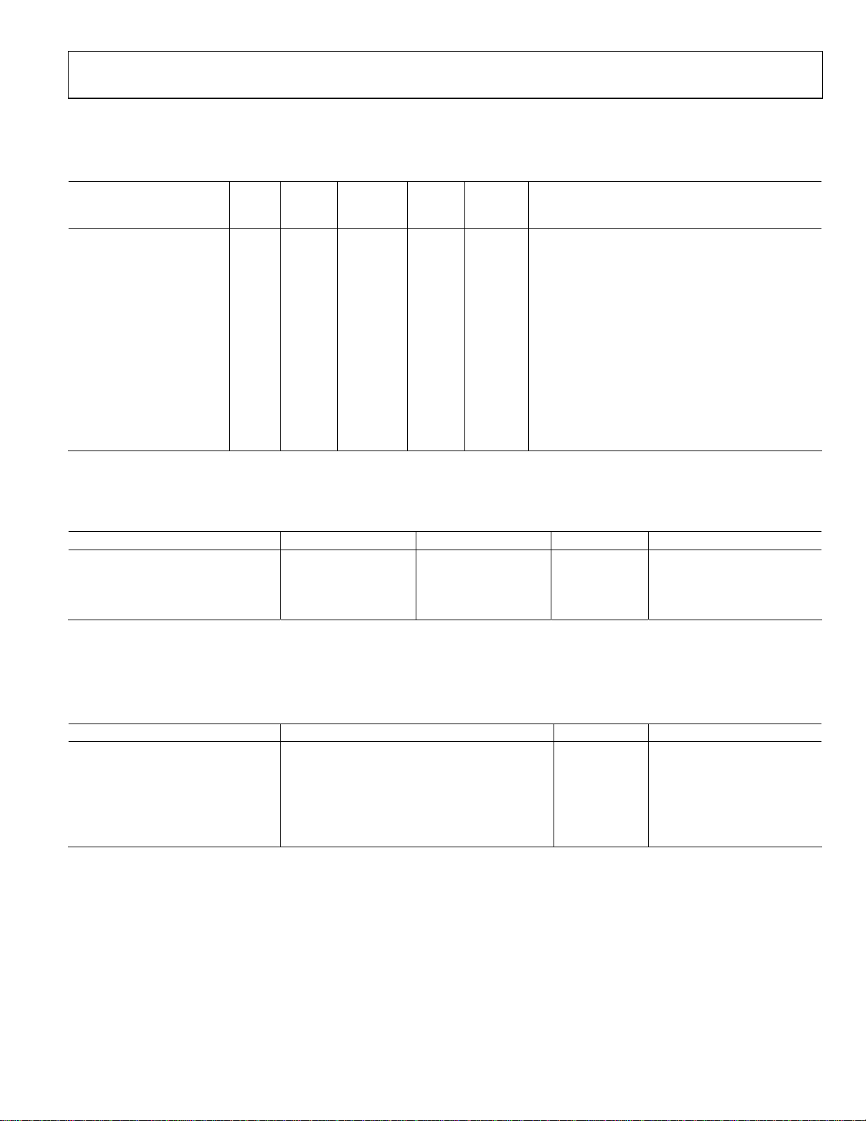
REFERENCE INPUT
Typical (typ) is given for VS = 3.3 V ± 10%, TA = 25°C, unless otherwise noted. Minimum (min) and maximum (max) values are given
over full V
Table 5.
Parameter Min Typ Max Unit Test Conditions/Comments
CLOCK INPUT (REFCLK)
Input Frequency 25 MHz
Input High Voltage 2.0 V
Input Low Voltage 0.8 V
Input Current −1.0 +1.0 μA
Input Capacitance 2 pF
and TA (−40°C to +85°C) variation.
S
Rev. B | Page 5 of 20

AD9572
CLOCK OUTPUTS
Typical (typ) is given for VS = 3.3 V ± 10%, TA = 25°C, unless otherwise noted. Minimum (min) and maximum (max) values are given
over full V
Table 6.
Parameter Min Typ Max Unit Test Conditions/Comments
LVPECL CLOCK OUTPUTS
Output Frequency 156.25 MHz
Output High Voltage (VOH) VS − 1.24 VS − 1.05 VS − 0.83 V
Output Low Voltage (VOL) VS − 2.07 VS − 1.87 VS − 1.62 V
Output Differential Voltage (VOD) 700 825 950 mV
Duty Cycle 45 55 %
LVDS CLOCK OUTPUTS
Output Frequency 156.25 MHz
Differential Output Voltage (VOD) 250 350 475 mV
Delta VOD 25 mV
Output Offset Voltage (VOS) 1.125 1.25 1.375 V
Delta VOS 25 mV
Short-Circuit Current (ISA, ISB) 14 24 mA Output shorted to GND
Duty Cycle 45 55 %
CMOS CLOCK OUTPUTS
Output Frequency 33.33 MHz
Output High Voltage (VOH) VS − 0.1 V Sourcing 1.0 mA current
Output Low Voltage (VOL) 0.1 V Sinking 1.0 mA current
Duty Cycle 42 58 %
and TA (−40°C to +85°C) variation.
S
TIMING CHARACTERISTICS
Typical (typ) is given for VS = 3.3 V ± 10%, TA = 25°C, unless otherwise noted. Minimum (min) and maximum (max) values are given
over full V
Table 7.
Parameter Min Typ Max Unit Test Conditions/Comments
LVPECL
Output Rise Time, tRP 480 625 810 ps 20% to 80%, measured differentially
Output Fall Time, tFP 480 625 810 ps 80% to 20%, measured differentially
LVDS
Output Rise Time, tRL 160 350 540 ps 20% to 80%, measured differentially
Output Fall Time, tFL 160 350 540 ps 80% to 20%, measured differentially
CMOS
Output Rise Time, tRC 0.25 0.50 2.5 ns
Output Fall Time, tFC 0.25 0.70 2.5 ns
Output Rise Time, t
Output Fall Time, t
and TA (−40°C to +85°C) variation.
S
1.3 2.1 2.6 ns
RC2
1.4 2.3 3.0 ns
FC2
Termination = 200 Ω to 0 V; C
= 0 pF; CAC = 100
LOAD
nF; oscilloscope set to 50 Ω termination
Termination = 100 Ω differential; C
= 0 pF; CAC =
LOAD
100 nF; oscilloscope set to 50 Ω termination
20% to 80%; termination = 50 Ω to 0 V; C
= 100 nF
C
AC
80% to 20%; termination = 50 Ω to 0 V; C
= 100 nF
C
AC
LOAD
LOAD
20% to 80%; active probe measurement, C
1 pF, R
probe
=20 kΩ, C
LOAD
= 3.9 pF
80% to 20%; active probe measurement, C
1 pF, R
probe
=20 kΩ, C
LOAD
= 3.9 pF
= 5 pF;
= 5 pF;
=
probe
=
probe
Rev. B | Page 6 of 20
 Loading...