Analog Devices AD9561JR-REEL, AD9561JR Datasheet

a
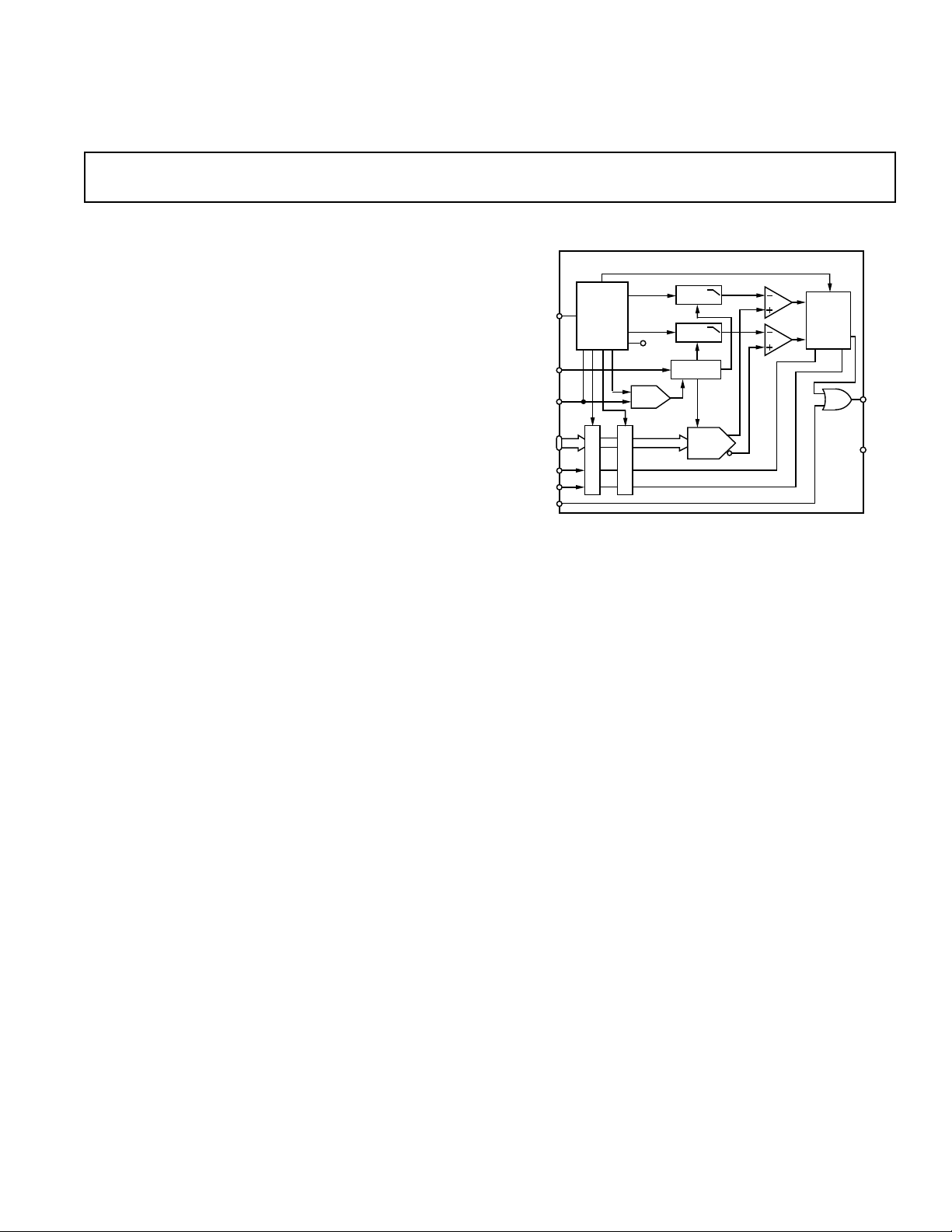
RAMP
RAMP
CLOCK
R
SET
CAL IN
8-BIT
DATA
SEM/DEM
LEM/TEM
RETRACE
REF
DAC
OUTPUT
LOGIC
PWM
OUT
CAL
DAC
INTERNAL
TIMING
L
A
T
C
H
L
A
T
C
H
AD9561
CAL
OUT
CAL
OUT
Pulse Width Modulator
AD9561
FEATURES
60 MHz Pulse Rate
8-Bit Resolution
Center, Left or Right Justify
Low Power: 700 mW typical
Minimum Pulse Width: <5 ns
Maximum PW: 100 % Full-scale
APPLICATIONS
Laser Printers
Digital Copiers
Color Copiers
GENERAL DESCRIPTION
The AD9561 is a second generation high speed, digitally
programmable pulse width modulator (PWM). Output pulse
width is proportional to an 8-bit DATA input value. Two
additional control inputs determine if the pulse is placed at the
beginning, middle or end of the clock period. Pulse width and
placement can be changed every clock cycle up to 60 MHz.
Pulse width modulation is a well proven method for controlling
gray scale and resolution enhancement in scanning laser print
engines. Modulating pulse width provides the most cost
effective method for continuous tone reproduction and resolu-
tion enhancement in low-to-moderate cost scanning electro-
photographic systems.
The AD9561 uses precision analog circuits to control dot size
so that near-photographic quality images are practical without
the high frequency clock signals required by all digital approaches.
The AD9561 has improved features and performance over its
predecessor, the AD9560. An improved ramp topology enables
control of pulse width through 100% of the dot clock period as
opposed to 95% for the AD9560. This enables smooth transi-
tion across dot boundaries for line screen applications.
FUNCTIONAL BLOCK DIAGRAM
Additionally, input data setup and hold time are symmetrical at
2 ns each, simplifying interface to the system bus.
Finally, chip design and pinout are optimized to decrease
sensitivity of analog circuits to digital coupling. (See layout
section for detailed recommendations for optimum results.)
Inputs are TTL or CMOS compatible, and outputs are CMOS
compatible. The AD9561JR is packaged in a 28-lead plastic
SOIC. It is rated over the commercial temperature range, 0°C
to +70°C.
HIGHLIGHTS
1. 60 MHz native printer clock rate.
2. Single +5 V power supply.
3. On-chip Autocalibration.
4. Pulse placement flexibility.
5. High resolution: 256 pulse widths.
REV. 0
Information furnished by Analog Devices is believed to be accurate and
reliable. However, no responsibility is assumed by Analog Devices for its
use, nor for any infringements of patents or other rights of third parties
which may result from its use. No license is granted by implication or
otherwise under any patent or patent rights of Analog Devices.
One Technology Way, P.O. Box 9106, Norwood, MA 02062-9106, U.S.A.
Tel: 617/329-4700 World Wide Web Site: http://www.analog.com
Fax: 617/326-8703 © Analog Devices, Inc., 1996

AD9561–SPECIFICATIONS
(+VS = +5 V; R
= 715 V, CLOCK = 20 MHz unless otherwise noted)
SET
AD9561JR
Parameter Temp Min Typ Max Units
RESOLUTION 8 Bits
ACCURACY (@ 20 MHz)
Differential Nonlinearity +25°C ±0.5 ±2 LSB
Integral Linearity
Odd/Even Pulse Mismatch
1
2
+25°C ± 1.5 ±4 LSB
+25°C ±0.75 LSB
DIGITAL INPUTS
Logic “1” Voltage Full 2.0 V
Logic “0” Voltage Full 0.8 V
Input Current Full ±1 µA
Input Capacitance
+25°C
5pF
Data Setup Time Full 2.0 0.3 ns
Data Hold Time Full 2.0 0.3 ns
Minimum Clock Pulse Width (HIGH) Full 6 ns
DYNAMIC PERFORMANCE
Maximum Trigger Rate Full 60 MHz
Minimum Propagation Delay (t
Minimum Propagation Delay TC Full 60 ps/°C
Output Pulse Width @ Code 25
Output Pulse Width @ Code 255 Full 100 % Clock
Output Rise Time
Output Fall Time
5, 6
5, 6
PD
3
)
4
+25°C122028ns
Full 5 ns
Full 1.8 3 ns
Full 1.8 3 ns
RETRACE Propagation Delay Full 6 ns
PWM OUTPUT
Logic “1” Voltage
Logic “0” Voltage
5, 6
5, 6
Full 4.6 V
Full 0.4 V
CAL OUT
Logic “1” Voltage Full 4.6 V
Logic “0” Voltage Full 0.4 V
POWER SUPPLY
7
Positive Supply Current (+5.0 V) Full 140 170 mA
Power Dissipation Full 700 850 mW
Power Reduce Current Full 70 85 mA
Power Reduce Dissipation Full 350 425 mW
Power Supply Rejection Ratio
Propagation Delay Sensitivity (TEM)
NOTES
1
Best Fit between codes 25 and 230. INL is very layout sensitive.
2
Due to linearity mismatch in dual ramps.
3
Measured from rising edge of clock to transition of Codes 0 to 255.
4
Minimum pulse width (at 20 MHz) limited by rise time. Pulse width for Code 25 will be greater when CLOCK < 20 MHz.
5
Output load = 10 pF and 2 mA source/sink.
6
Load conditions to test output drive capability. Linearity will degrade with either capacitive or current loading. Best linearity obtained driving a single CMOS input.
7
All performance specifications valid when supply maintained at +5 V, ±5%.
8
Tested from +4.75 V to +5.25 V.
Specification subject to change without notice.
8
+25°C 1.5 ns/V
–2–
REV. 0

AD9561
28
27
26
22
21
20
19
18
17
25
24
23
TOP VIEW
(Not to Scale)
1
2
3
7
8
9
10
11
12
4
5
6
13
14
16
15
AD9561
OUT
V
DD
D2
D1
GND
V
DD
RETRACE
CAL START
V
DD
GND
D0 (LSB)
LEM/TEM
SEM/DEM
GND
D3
D4
D5
V
DD
GND
V
DD
CAL OUT
GND
D7(MSB)
CLOCK
GND
R
SET
D6
PWR REDUCE
WARNING!
ESD SENSITIVE DEVICE
ABSOLUTE MAXIMUM RATINGS
1
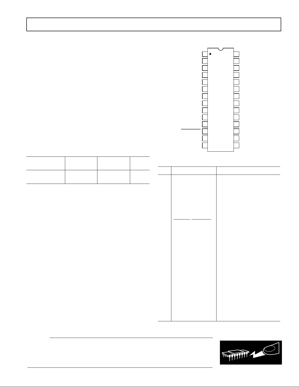
PIN CONFIGURATION
Positive Supply Voltage . . . . . . . . . . . . . . . . . . . . . . . . . . +7 V
Digital Input Voltage Range . . . . . . . . . . . . . . . –0.5 V to V
Minimum R
Digital Output Current (Sourcing)
Digital Output Current (Sinking)
Operating Temperature Range
. . . . . . . . . . . . . . . . . . . . . . . . . . . . . . . 120 Ω
SET
2
. . . . . . . . . . . . . . . 10 mA
2
. . . . . . . . . . . . . . . . 10 mA
3
. . . . . . . . . . . . . 0°C to +70°C
DD
Storage Temperature Range . . . . . . . . . . . . –65°C to +150°C
Junction Temperature . . . . . . . . . . . . . . . . . . . . . . . . .+150°C
Lead Soldering Temperature (10 sec)
NOTES
1
Absolute maximum ratings are limiting values, to be applied individually, and
beyond which serviceability may be impaired. Functional operation under any of
these conditions is not necessarily implied.
2
CAL OUT should drive a single TTL or CMOS input.
3
Typical Thermal Impedance:
28-lead SOIC (plastic) θJA = 71.4 °C/W; θJC = 23°C/W.
4
When soldering surface mount packages in vapor phase equipment, temperature
should not exceed 220°C for more than one minute.
4
. . . . . . . . . . . .+300°C
ORDERING GUIDE
Temperature Package Package
PIN DESCRIPTIONS
Model Range Description Option
Pin Name Description
AD9561JR 0°C to +70°C 28-Lead SOIC R-28
AD9561JR-REEL* 0°C to +70°C 28-Lead SOIC R-28
*Tape and Reel ordered in multiples of 1000 ICs.
1–5 D3–D7 Digital Data Bits, D7 Is MSB
6 CLOCK Clock Input
7V
DD
8 GND Ground Return
9V
DD
10 GND Ground Return
11 CAL OUT Calibration Complete Output
12
POWER REDUCE Place AD9561 in Sleep Mode
13 GND Ground Return
14 R
SET
15 GND Ground Return
16 V
DD
17 CAL START Initiates Calibration Cycle
18 RETRACE Force Output High
19 V
DD
20 GND Ground Return
21 OUT Modulated Pulse Out
22 GND Ground Return
CAUTION
ESD (electrostatic discharge) sensitive device. Electrostatic charges as high as 4000 V readily
accumulate on the human body and test equipment and can discharge without detection.
Although the AD9561 features proprietary ESD protection circuitry, permanent damage may
occur on devices subjected to high energy electrostatic discharges. Therefore, proper ESD
precautions are recommended to avoid performance degradation or loss of functionality.
REV. 0
23 V
DD
24 LEM/TEM Controls Leading (1) or
25 SEM/DEM Controls Single (1) or Dual (0)
26–28 D0–D2 Digital Data Bits, D0 is LSB
–3–
+5 V Supply
+5 V Supply
Ramp Current Set Resistor
+5 V Supply
+5 V Supply
+5 V Supply
Trailing (0) Edge Modulation
Edge Modulation
