Flexible Clock Translator for GPON, Base
AD9553
PLL
OUTPUT
CIRCUITRY
INPUT
FREQUENCY
SOURCE
SELECTOR
REFA
REFB
XTAL
OUT2
OUT1
PIN-DEFINED AND SERIAL P ROGRAMMING
AD9553
08565-001
Station, SONET/SDH, T1/E1, and Ethernet
FEATURES
Input frequencies from 8 kHz to 710 MHz
Output frequencies up to 810 MHz LVPECL and LVDS (up to
200 MHz for CMOS output)
Preset pin-programmable frequency translation ratios cover
popular wireline and wireless frequency applications,
including xDSL, T1/E1, BITS, SONET, and Ethernet
Arbitrary frequency translation ratios via SPI port
On-chip VCO
Accepts a crystal resonator for holdover applications
Two single-ended (or one differential) reference input(s)
Two output clocks (independently programmable as LVDS,
LVPEC L, or CMOS)
SPI-compatible, 3-wire programming interface
Single supply (3.3 V)
Very low power: <450 mW (under most conditions)
Small package size (5 mm × 5 mm)
Exceeds Telcordia GR-253-CORE jitter generation, transfer,
and tolerance specifications
APPLICATIONS
Cost effective replacement of high frequency VCXO, OCXO,
and SAW resonators
Extremely flexible frequency translation for SONET/SDH,
Ethernet, Fibre Channel, DRFI/DOCSIS, and
PON/EPON/GPON
Wireless infrastructure
Test and measurement (including handheld devices)
GENERAL DESCRIPTION
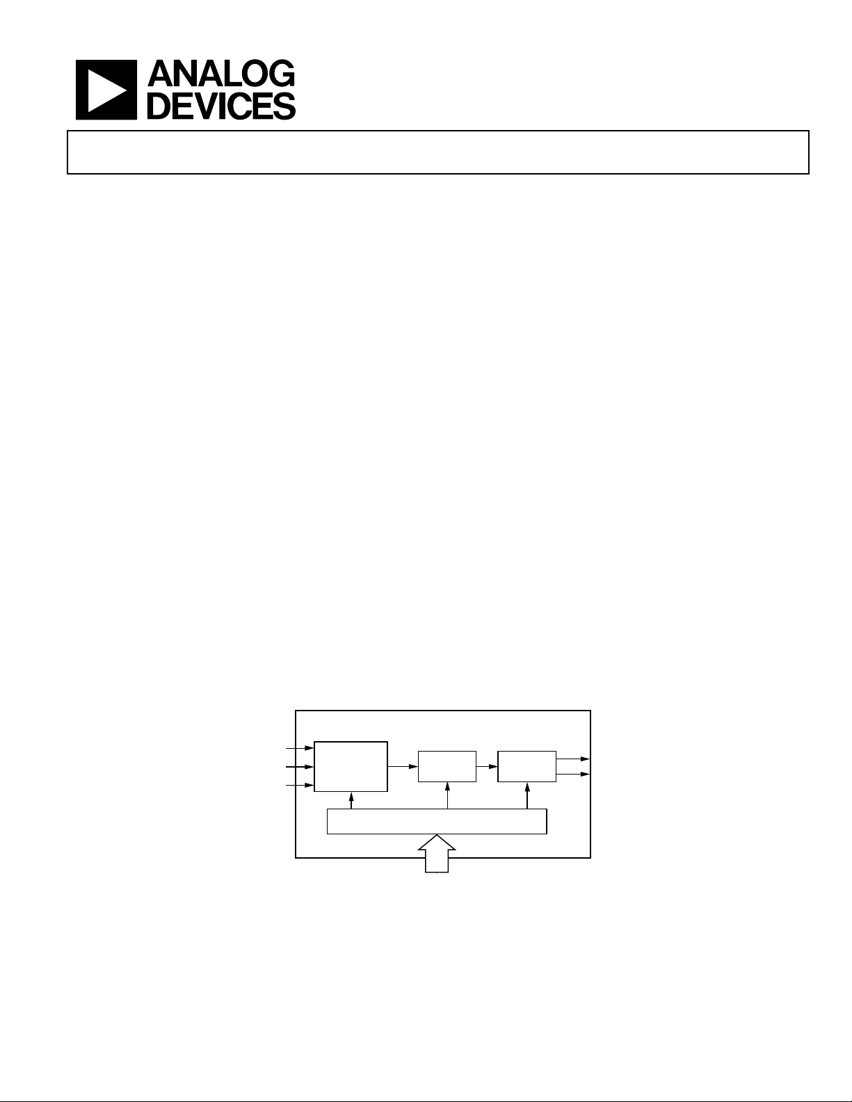
The AD9553 is a phase-locked loop (PLL) based clock translator
designed to address the needs of passive optical networks (PON)
and base stations. The device employs an integer-N PLL to
accommodate the applicable frequency translation requirements.
The user supplies up to two single-ended input reference signals or
one differential input reference signal via the REFA and REFB
inputs. The device supports holdover applications by allowing the
user to connect a 25 MHz crystal resonator to the XTAL input.
The AD9553 is pin programmable, providing a matrix of standard
input/output frequency translations from a list of 15 possible input
frequencies to a list of 52 possible output frequency pairs (OUT1
and OUT2). The device also has a 3-wire SPI interface, enabling
the user to program custom input-to-output frequency translations.
The AD9553 output drivers are compatible with LVPECL, LVDS,
or single-ended CMOS logic levels, although the AD9553 is
implemented in a strictly CMOS process.
The AD9553 operates over the extended industrial temperature
range of −40°C to +85°C.
BASIC BLOCK DIAGRAM
Rev. A
Information furnished by Analog Devices is believed to be accurate and reliable. However, no
responsibility is assumed by Analog Devices for its use, nor for any infringements of patents or other
rights of third parties that may result from its use. Specifications subject to change without notice. No
licen se is granted by implication or otherwise under any patent or patent rights of Analog Devices.
Trademarks and registered trademarks are the property of their respective owners.
Figure 1.
One Technology Way, P.O. Box 9106, Norwood, MA 02062-9106, U.S.A.
Tel: 781.329.4700
Fax: 781.461.3113 ©2010 Analog Devices, Inc. All rights reserved.
www.analog.com
 Loading...