

R
Multiservice Clock Generator
FEATURES
Translation between any two standard network rates
Dual reference inputs and dual clock outputs
Pin programmable for standard network rate translation
SPI programmable for arbitrary rational rate translation
Output frequencies from 10 MHz to 900 MHz
Input frequencies from 19.44 MHz to 806 MHz
On-chip VCO
Meets OC-192 high band jitter generation requirement
Supports standard forward error correction (FEC) rates
Supports holdover operation
Supports hitless switchover and phase build-out (even with
unequal reference frequencies)
SPI-compatible 3-wire programming interface
Single supply (3.3 V)
APPLICATIONS
Multiservice switches
Multiservice routers
Exact network clock frequency translation
General-purpose frequency translation
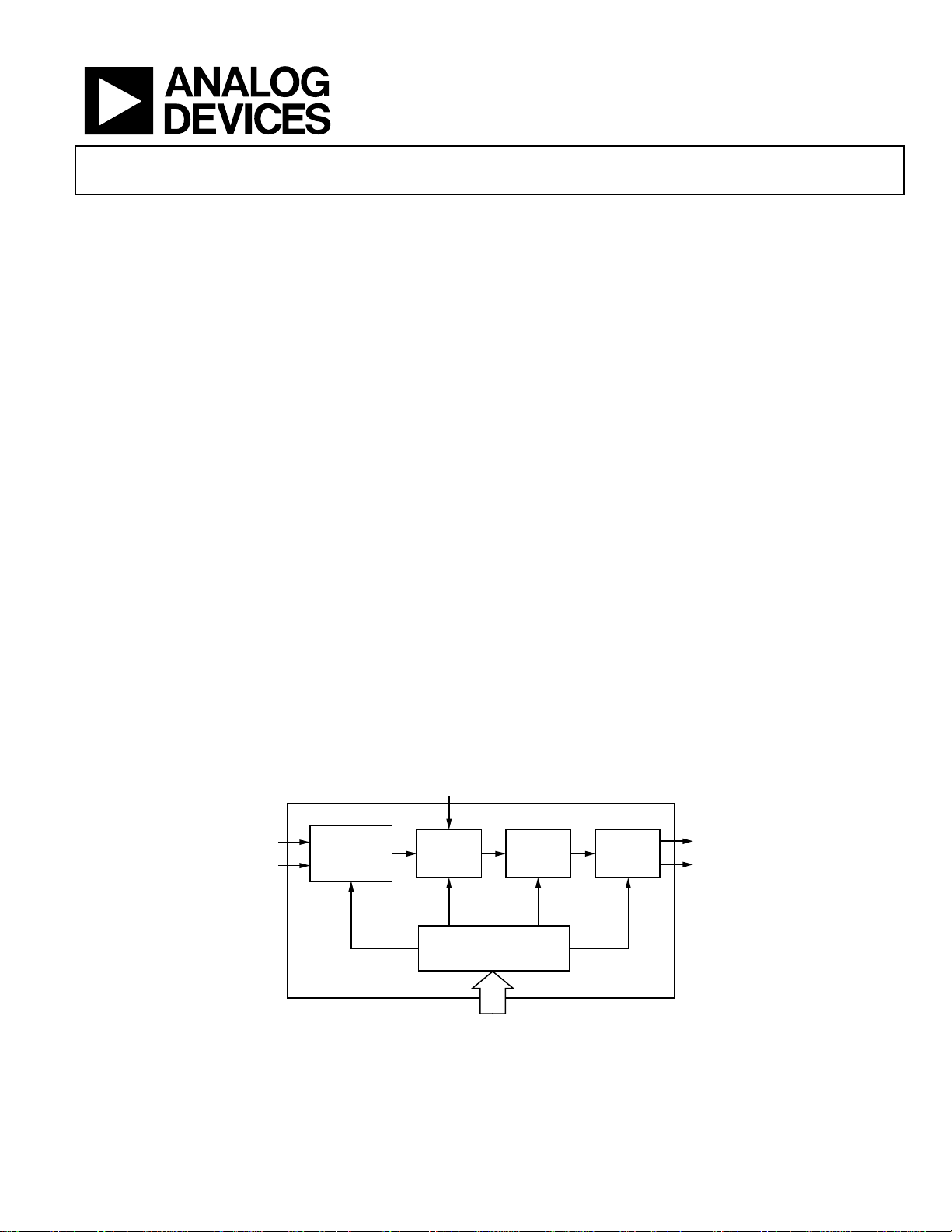
GENERAL DESCRIPTION
The AD9551 accepts one or two reference input signals to synthesize one or two output signals. The AD9551 uses a fractional-N
PLL that precisely translates the reference frequency to the desired
output frequency. The input receivers and output drivers provide
both single-ended and differential operation.
AD9551
Reference conditioning and switchover circuitry internally
synchronizes the two references so that if one reference fails,
there is virtually no phase perturbation at the output.
The AD9551 uses an external crystal and an internal DCXO to
provide for holdover operation. If both references fail, the device
maintains a steady output signal.
The AD9551 provides pin-selectable, preset divider values for
standard (and FEC adjusted) network frequencies. The pinselectable frequencies include any combination of 15 possible
input frequencies and 16 possible output frequencies. A SPI
interface provides further flexibility by making it possible to
program almost any rational input/output frequency ratio.
The AD9551 is a clock generator that employs fractional-N-based
phase-locked loops (PLL) using sigma-delta (Σ-) modulators
(SDMs). The fractional frequency synthesis capability enables
the device to meet the frequency and feature requirements for
multiservice switch applications. The AD9551 precisely generates
a wide range of standard frequencies when using any one of those
same standard frequencies as a timing base (reference). The
primary challenge of this function is the precise generation of the
desired output frequency because even a slight output frequency
error can cause problems for downstream clocking circuits in
the form of bit or cycle slips. The requirement for exact frequency
translation in such applications necessitates the use of a fractional-N-based PLL architecture with variable modulus.
BASIC BLOCK DIAGRAM
C
YSTAL
(26MHz)
REFA
REFB
Rev. B
Information furnished by Analog Devices is believed to be accurate and reliable. However, no
responsibility is assumed by Analog Devices for its use, nor for any infringements of patents or other
rights of third parties that may result from its use. Specifications subject to change without notice. No
license is granted by implication or otherwise under any patent or patent rights of Analog Devices.
Trademarks and registered trademarks ar
e the property of their respective owners.
REFERENCE
CONDITIONING
AND SWITCH-
OVER
HOLDOVER
LOOP
PIN-DEFINED AND SERIAL
PROGRAMMING
Figure 1.
One Technology Way, P.O. Box 9106, Norwood, MA 02062-9106, U.S.A.
Tel: 781.329.4700 www.analog.com
Fax: 781.461.3113 ©2009 Analog De
PLL
OUTPUT
CIRCUITRY
AD9551
OUT1
OUT2
07805-001
vices, Inc. All rights reserved.

AD9551
TABLE OF CONTENTS
Features .............................................................................................. 1
Applications ....................................................................................... 1
General Description ......................................................................... 1
Basic Block Diagram ........................................................................ 1
Revision History ............................................................................... 2
Functional Block Diagram .............................................................. 3
Specifications ..................................................................................... 4
Reference Clock Input Characteristics ...................................... 4
Output Characteristics ................................................................. 4
Jitter Characteristics (180 Hz Loop Bandwidth) ...................... 5
Crystal Oscillator Characteristics............................................... 5
Power Consumption .................................................................... 5
Logic Input Pins ............................................................................ 6
RESET Pin ..................................................................................... 6
Logic Output Pins ......................................................................... 6
Serial Control Port ....................................................................... 6
Serial Control Port Timing ......................................................... 7
Absolute Maximum Ratings ............................................................ 8
ESD Caution .................................................................................. 8
Pin Configuration and Function Descriptions ............................. 9
Typical Performance Characteristics ........................................... 11
Preset Frequency Ratios ................................................................. 14
Theory of Operation ...................................................................... 16
Operating Modes ........................................................................ 16
Component Blocks ..................................................................... 16
Holdover Mode ........................................................................... 21
Jitter Tolerance ............................................................................ 21
External Loop Filter Capacitor ................................................. 21
Output/Input Frequency Relationship .................................... 21
Calculating Divider Values ....................................................... 22
Low Dropout (LDO) Regulators .............................................. 24
Applications Information .............................................................. 25
Thermal Performance ................................................................ 25
Serial Control Port ......................................................................... 26
Serial Control Port Pin Descriptions ....................................... 26
Operation of the Serial Control Port ....................................... 26
Instruction Word (16 Bits) ........................................................ 27
MSB/LSB First Transfers ........................................................... 27
Register Map ................................................................................... 29
Register Map Descriptions ........................................................ 32
Outline Dimensions ....................................................................... 40
Ordering Guide .......................................................................... 40
REVISION HISTORY
9/09—Rev. A to Rev. B
Changes to Table 25 ........................................................................ 33
6/09—Rev. 0 to Rev. A
Changes to Figure 23 ...................................................................... 23
4/09—Revision 0: Initial Version
Rev. B | Page 2 of 40
AD9551
L
A
The AD9551 is easily configured using the external control pins
(A[3:0], B[3:0], and Y[3:0]). The logic state of these pins sets predefined divider values that establish a specific input-to-output
frequency ratio. For applications requiring other frequency ratios,
the user can override any of the preconfigured divider settings
via the serial port, which enables a very wide range of
applications.
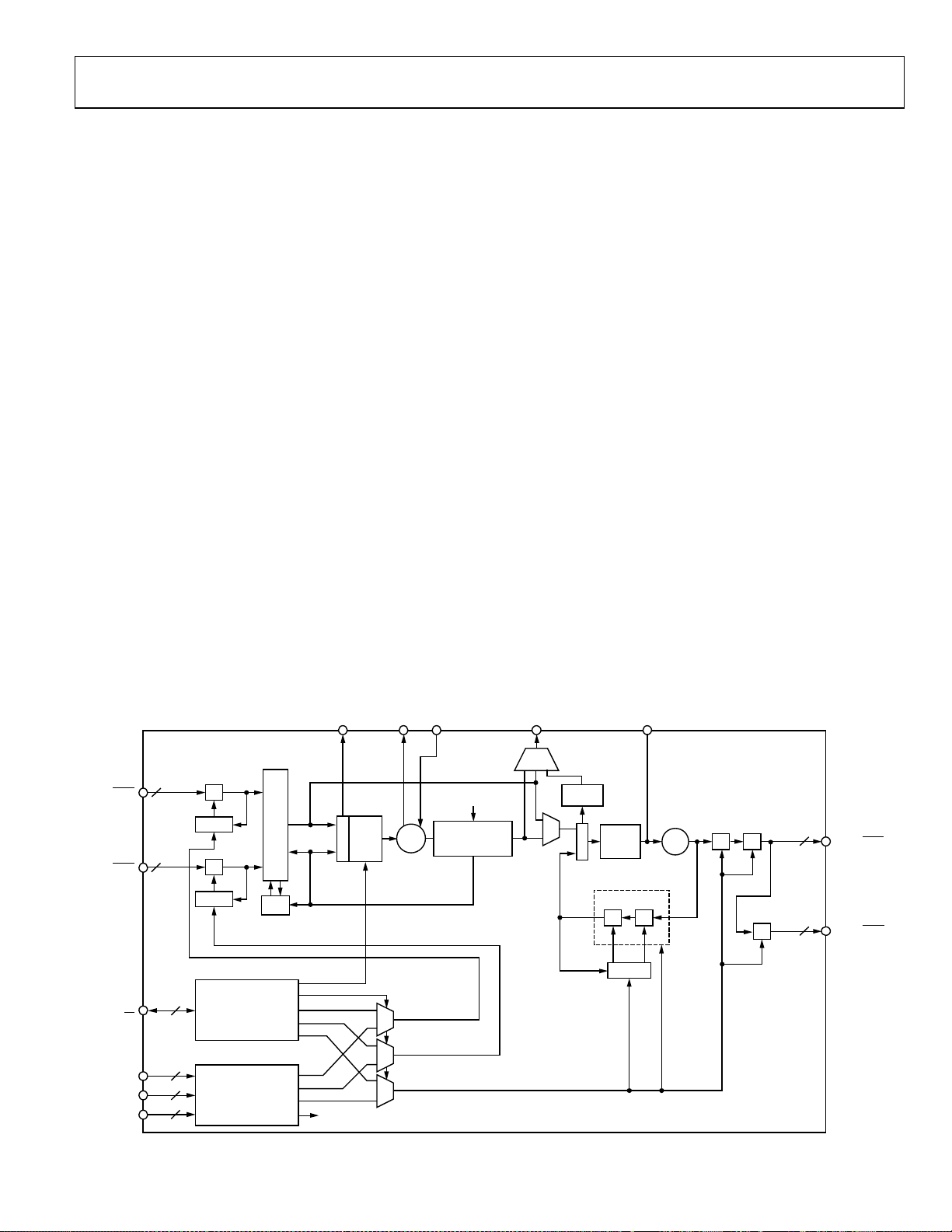
The AD9551 architecture consists of two cascaded PLL stages.
The first stage consists of fractional division (via SDM), followed
by a digital PLL that uses a crystal resonator-based DCXO. The
DCXO relies on an external crystal with a resonant frequency in
the range of 19.44 MHz to 52 MHz. The DCXO constitutes the
first PLL, which operates within a narrow frequency range
(±50 ppm) around the crystal resonant frequency. This PLL has
a loop bandwidth of approximately 180 Hz, providing initial jitter
cleanup of the input reference signal. The second stage is a frequency multiplying PLL that translates the first stage output
frequency (in the range of 19.44 MHz to 104 MHz) up to
~3.7 GHz. This PLL incorporates an SDM-based fractional
feedback divider that enables fractional frequency multiplication.
Programmable integer dividers at the output of this second PLL
establish a final output frequency of up to 900 MHz.
It is important to understand that the architecture of the AD9551
produces an output frequency that is most likely not coherent
with the input reference frequency. The reason is that the input
and crystal frequencies typically are not harmonically related
and neither are the output and crystal frequencies. As a result,
there is generally no relationship between the phase of the input
and output signals.
FUNCTIONAL BLOCK DIAGRAM
INPUT PL
LOCKED
XTAL1 XTAL0 LF
The AD9551 includes reference signal processing blocks that
enable a smooth switching transition between two reference
inputs. This circuitry automatically detects the presence of the
reference input signals. If only one input is present, the device
uses it as the active reference. If both inputs are present, one
becomes the active reference and the other becomes the alternate reference. The circuitry edge-aligns the backup reference
with the active reference. If the active reference fails, the circuitry
automatically switches to the backup reference (if available),
making it the new active reference. Meanwhile, if the failed
reference is once again available, it becomes the new backup
reference and is edge-aligned with the new active reference
(a precaution against failure of the new active reference).
If neither reference can be used, the AD9551 supports a holdover
mode. Note that the external crystal is necessary to provide the
switchover and holdover functionality. It is also the clock source
for the reference synchronization and monitoring functions.
The AD9551 relies on a single external capacitor for the output
PLL loop filter. With proper termination, the output is compatible
with LVPECL, LVDS, or CMOS logic levels, although the AD9551
is implemented in a strictly CMOS process.
The AD9551 operates over the extended industrial temperature
range of −40°C to +85°C.
OUTPUT PLL
LOCKED
REFA, REF
REFB, REFB
SCLK, SDIO,
A[3:0]
B[3:0]
Y[3:0]
TEST
MUX
f
2
REFA
N
A
SDM
A
f
2
REFB
N
B
SDM
B
3
4
4
4
REGISTER BANK
PRECONFIGURED
DIVIDER V ALUES
CS
SYNCHRONI ZATIO N AND
SWITCH OVER CONTRO L
REFERENCE
MONITOR
SAMPLE RATE
CONTROL
DIG.
P
LOOP
F
D
FILTER
19.44MHz MODE
19.44MHz MODE
DCXO
NA, MODA, FRAC
NB, MODB, FRAC
N, MOD, FRAC, P0, P1, P
LOOP
CONFIGURATION
A
B
2
LOCK
DETECT
f
IF
P
F
D
CHARGE
PUMP
N = 4N
N1 4/5
SDM
+ N
1
FRAC, MOD
3350MHz TO
4050MHz
VCO
0
N
P2, P1, P
AD9551
4 TO111 TO
P
0P1
0
63
1 TO
63
P
f
2
OUT1
f
OUT2
2
2
OUT1, OUT1
OUT2, OUT2
07805-002
Figure 2.
Rev. B | Page 3 of 40
AD9551
SPECIFICATIONS
Minimum and maximum values apply for full range of supply voltage and operating temperature variation. Typical values apply for VDD = 3.3 V,
T
= 25°C, unless otherwise noted.
A
REFERENCE CLOCK INPUT CHARACTERISTICS
Table 1.
Parameter Min Typ Max Unit Test Conditions/Comments
FREQUENCY RANGE 19
INPUT CAPACITANCE 3 pF
INPUT RESISTANCE 6 kΩ Measured single-ended
DUTY CYCLE 40 60 %
REFERENCE CLOCK INPUT VOLTAGE SWING
Differential 250 mV Maximum magnitude across pin pair
Single-Ended 250 mV Peak-to-peak
1
The 19 MHz lower limit applies only to the 19.44 MHz operating mode.
OUTPUT CHARACTERISTICS
Table 2.
Parameter Min Typ Max Unit Test Conditions/Comments
LVPECL MODE
Differential Output Voltage Swing
Common-Mode Output Voltage VDD − 1.77 VDD − 1.66 VDD − 1.20 V Output driver static
Frequency Range 0 900 MHz
Duty Cycle 40 60 % Up to 805 MHz output frequency
Rise/Fall Time1 (20% to 80%) 255 305 ps
LVDS MODE
Differential Output Voltage Swing
Balanced, VOD 247 454 mV
Unbalanced, ∆VOD 25 mV
Offset Voltage
Common Mode, VOS 1.125 1.375 V Output driver static
Common-Mode Difference, ∆VOS 25 mV
Short-Circuit Output Current 17 24 mA
Frequency Range 0 900 MHz
Duty Cycle 40 60 % Up to 805 MHz output frequency
Rise/Fall Time1 (20% to 80%) 285 355 ps
CMOS MODE
Output Voltage High, VOH
IOH = 10 mA 2.8 V
IOH = 1 mA 2.8 V
Output Voltage Low, VOL
IOL = 10 mA 0.5 V
IOL = 1 mA 0.3 V
Frequency Range 0 200 MHz
1
806 MHz
Measured with a differential probe across
the input pins
690 765 889 mV Output driver static
100 Ω termination between both pins of
the output driver
Voltage swing between output pins;
output driver static
Absolute difference between voltage
swing of normal pin and inverted pin;
output driver static
Voltage difference between output pins;
output driver static
100 Ω termination between both pins of
the output driver
Output driver static; standard drive
strength setting
Output driver static; standard drive
strength setting
3.3 V CMOS; standard drive strength
setting
Rev. B | Page 4 of 40
AD9551
Parameter Min Typ Max Unit Test Conditions/Comments
Duty Cycle 45 55 % At maximum output frequency
Rise/Fall Time1 (20% to 80%) 500 745 ps
1
The listed values are for the slower edge (rise or fall).
JITTER CHARACTERISTICS (180 HZ LOOP BANDWIDTH)
Table 3.
Parameter Min Typ Max Unit Test Conditions/Comments
JITTER GENERATION
12 kHz to 20 MHz 1.3 ps rms fIN = 19.44 MHz, f
0.8 ps rms fIN = 622.08 MHz, f
50 kHz to 80 MHz 0.5 ps rms fIN = 19.44 MHz, f
0.6 ps rms fIN = 622.08 MHz, f
4 MHz to 80 MHz 0.1 ps rms fIN = 622.08 MHz, f
JITTER TRANSFER BANDWIDTH 180 Hz
JITTER TRANSFER PEAKING 0.1 dB
CRYSTAL OSCILLATOR CHARACTERISTICS
3.3 V CMOS; standard drive strength
setting; 10 pF load
= 622.08 MHz
OUT
= 622.08 MHz
OUT
= 622.08 MHz
OUT
= 622.08 MHz
OUT
= 622.08 MHz
OUT
See the Typical Performance
Characteristics section
See the Typical Performance
Characteristics section
Table 4.
Parameter Min Typ Max Unit Test Conditions/Comments
CRYSTAL FREQUENCY
Range 19 26 52 MHz
Tolerance 20 ppm
CRYSTAL MOTIONAL RESISTANCE 100 Ω
DCXO LOAD CAPACITANCE CONTROL
RANGE
3 to 21 pF
Requires a crystal with a 10 pF load
specification
POWER CONSUMPTION
Table 5.
Parameter Min Typ Max Unit Test Conditions/Comments
TOTAL CURRENT 169 195 mA
VDD CURRENT BY PIN
Pin 9 24 27 mA
Pin 23 78 84 mA
Pin 27 36 42 mA
Pin 34 36 42 mA
LVPECL OUTPUT DRIVER 38 mA
At maximum output frequency with both
output channels active
900 MHz with 100 Ω termination between
both pins of the output driver
Rev. B | Page 5 of 40
AD9551
LOGIC INPUT PINS
Table 6.
Parameter Min Typ Max Unit Test Conditions/Comments
INPUT CHARACTERISTICS
Logic 1 Voltage, VIH 1.0 V
Logic 0 Voltage, VIL 0.8 V
Logic 1 Current, IIH 3 µA
Logic 0 Current, IIL 17 µA
1
The A[3:0], B[3:0], Y[3:0], and OUTSEL pins have 100 kΩ internal pull-up resistors.
RESET PIN
Table 7.
Parameter Min Typ Max Unit
INPUT CHARACTERISTICS
Input Voltage High, VIH 1.8 V
Input Voltage Low, VIL 1.3 V
Input Current High, I
Input Current Low, I
MINIMUM PULSE WIDTH HIGH 2 ns
1
The RESET pin has a 100 kΩ internal pull-up resistor, so the default state of the device is reset.
1
For the CMOS inputs, a static Logic 1 results
from either a pull-up resistor or no connection
1
0.3 12.5 µA
INH
31 43 µA
INL
LOGIC OUTPUT PINS
Table 8.
Parameter Min Typ Max Unit
OUTPUT CHARACTERISTICS
Output Voltage High, VOH 2.7 V
Output Voltage Low, VOL 0.4 V
SERIAL CONTROL PORT
Table 9.
Parameter Min Typ Max Unit Test Conditions/Comments
CS
Input Logic 1 Voltage 1.6 V
Input Logic 0 Voltage 0.5 V
Input Logic 1 Current 0.03 µA
Input Logic 0 Current 2 µA
Input Capacitance 2 pF
SCLK
Input Logic 1 Voltage 1.6 V
Input Logic 0 Voltage 0.5 V
Input Logic 1 Current 2 µA
Input Logic 0 Current 0.03 µA
Input Capacitance 2 pF
SDIO
Input
Input Logic 1 Voltage 1.6 V
Input Logic 0 Voltage 0.5 V
Rev. B | Page 6 of 40
AD9551
Parameter Min Typ Max Unit Test Conditions/Comments
Input Logic 1 Current 1 µA
Input Logic 0 Current 1 µA
Input Capacitance 2 pF
Output
Output Logic 1 Voltage 2.8 V 1 mA load current
Output Logic 0 Voltage 0.3 V 1 mA load current
SERIAL CONTROL PORT TIMING
Table 10.
Parameter Limit Unit
SCLK
Clock Rate, 1/t
Pulse Width High, t
Pulse Width Low, t
SDIO to SCLK Setup, tDS 4 ns min
SCLK to SDIO Hold, tDH 0 ns min
SCLK to Valid SDIO, tDV 13 ns max
CS to SCLK Setup (tS) and Hold (tH)
CS Minimum Pulse Width High
50 MHz max
CLK
3 ns min
HIGH
3 ns min
LOW
0 ns min
6.4 ns min
Rev. B | Page 7 of 40
AD9551
ABSOLUTE MAXIMUM RATINGS
Table 11.
Parameter Rating
Supply Voltage (VDD) 3.6 V
Maximum Digital Input Voltage −0.5 V to VDD + 0.5 V
Storage Temperature −65°C to +150°C
Operating Temperature Range −40°C to +85°C
Lead Temperature (Soldering, 10 sec) 300°C
Junction Temperature 150°C
Stresses above those listed under Absolute Maximum Ratings
may cause permanent damage to the device. This is a stress
rating only; functional operation of the device at these or any
other conditions above those indicated in the operational
section of this specification is not implied. Exposure to absolute
maximum rating conditions for extended periods may affect
device reliability.
ESD CAUTION
Rev. B | Page 8 of 40
AD9551
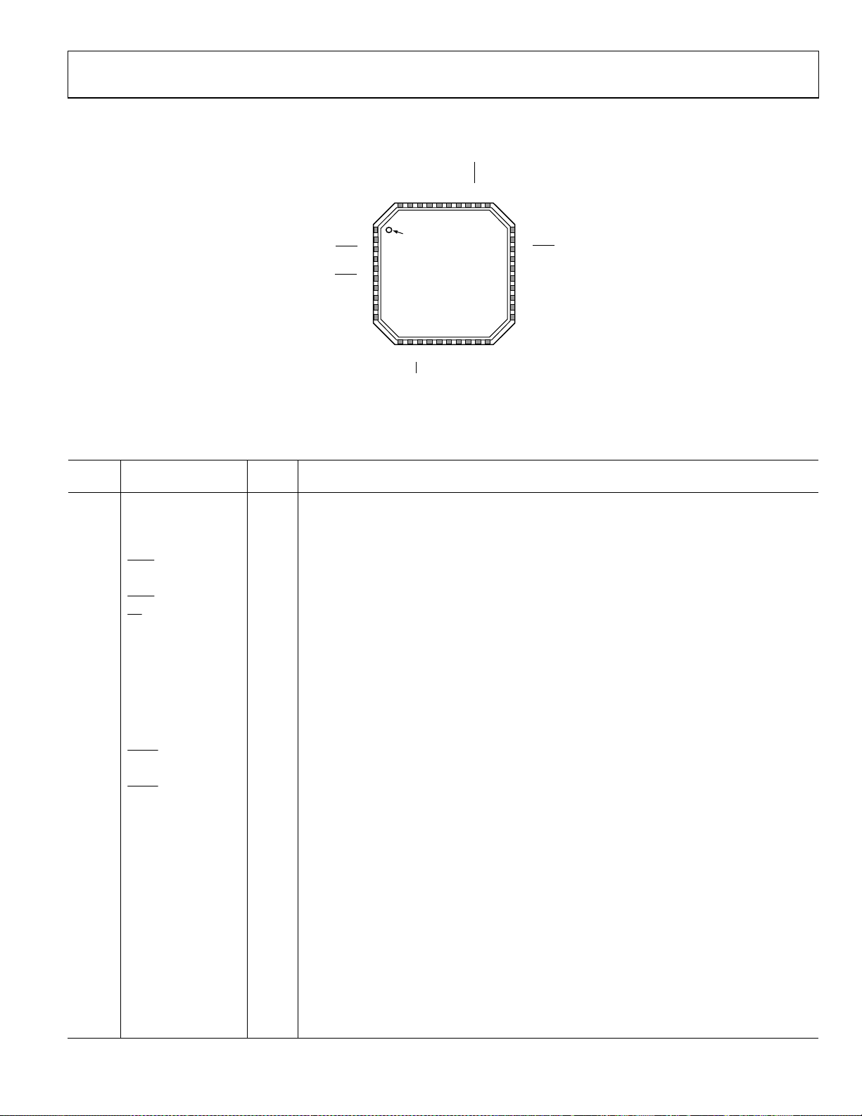
PIN CONFIGURATION AND FUNCTION DESCRIPTIONS
A2
A3
B0
B1
37
38
39
40
PIN 1
1B2
INDICATOR
2B3
3
REFA
4REFA
5REFB
6
REFB
7RESET
8LDO_IPDIG
9VDD
10LDO_XTAL
NOTES
1. EXPOSED DI E PAD MUST BE CONNECTED TO GND.
AD9551
TOP VIEW
(Not to Scale)
11
12
13
CS
XTAL0
XTAL1
14
SCLK
Figure 3. Pin Configuration
Table 12. Pin Function Descriptions
Pin
No.
9, 23,
Mnemonic Type
VDD P Power Supply Connection (3.3 V Analog Supply).
1
Description
27, 34
30, 31 GND P Analog Ground.
4 REFA I Analog Input (Active High)—Reference Clock Input A.
3
REFA
I Analog Input (Active High)—Complementary Reference Clock Input A.
5 REFB I Analog Input (Active High)—Reference Clock Input B.
6
13
REFB
CS
I Analog Input (Active High)—Complementary Reference Clock Input B.
I Digital Input Chip Select (Active Low).
14 SCLK I Serial Data Clock.
15 SDIO I/O Digital Serial Data Input/Output.
7 RESET I
Digital Input (Active High). Resets internal logic to default states. This pin has an internal 100 kΩ
pull-up resistor, so the default state of the device is reset.
11 XTL0 I Pin for Connecting an External Crystal (20 MHz to 30 MHz).
12 XTL1 I Pin for Connecting an External Crystal (20 MHz to 30 MHz).
33 OUT1 O Square Wave Clocking Output 1.
32
OUT1
O Complementary Square Wave Clocking Output 1.
29 OUT2 O Square Wave Clocking Output 2.
28
OUT2
17 LF I/O
O Complementary Square Wave Clocking Output 2.
Loop Filter Node for the Output PLL. Connect an external 12 nF capacitor (100 nF in 19.44 MHz
mode) from this pin to Pin 22 ( LDO_VCO).
26 OUTPUT PLL LOCKED O Active High Locked Status Indicator for the Output PLL.
25 INPUT PLL LOCKED O Active High Locked Status Indicator for the Input PLL.
16 OUTSEL I
Logic 0 selects LVDS, and Logic 1 selects LVPECL-compatible levels for both OUT1 and OUT2
when the outputs are not under SPI port control. Can be overridden via the programming registers.
8 LDO_IPDIG P/O LDO Decoupling Pin. Connect a 0.47 F decoupling capacitor from this pin to ground.
10 LDO_XTAL P/O LDO Decoupling Pin. Connect a 0.47 F decoupling capacitor from this pin to ground.
22 LDO_VCO P/O LDO Decoupling Pin. Connect a 0.47 F decoupling capacitor from this pin to ground.
24 LDO_1.8 P/O LDO Decoupling Pin. Connect a 0.47 F decoupling capacitor from this pin to ground.
35 A0 I Control Pin. Selects preset values for the REFA dividers.
36 A1 I Control Pin. Selects preset values for the REFA dividers.
37 A2 I Control Pin. Selects preset values for the REFA dividers.
38 A3 I Control Pin. Selects preset values for the REFA dividers.
1
ND
OUT1
VDD
A0
A1
OUT
G
32
31
33
34
35
36
30 GND
29 OUT2
28
OUT2
27 VDD
26 OUT PUT PLL LOCKED
25 INPUT PLL LOCKED
24 LDO _1.8
23 VDD
22 LDO_VCO
21 Y0
15
17
16
18
19
20
LF
Y3
Y2
SDIO
Y1
UTSEL
O
07805-003
Rev. B | Page 9 of 40

AD9551
Pin
No. Mnemonic Type
39 B0 I Control Pin. Selects preset values for the REFB dividers.
40 B1 I Control Pin. Selects preset values for the REFB dividers.
1 B2 I Control Pin. Selects preset values for the REFB dividers.
2 B3 I Control Pin. Selects preset values for the REFB dividers.
21 Y0 I Control Pin. Selects preset values for the output PLL feedback dividers and OUT1 dividers.
20 Y1 I Control Pin. Selects preset values for the output PLL feedback dividers and OUT1 dividers.
19 Y2 I Control Pin. Selects preset values for the output PLL feedback dividers and OUT1 dividers.
18 Y3 I Control Pin. Selects preset values for the output PLL feedback dividers and OUT1 dividers.
EP Exposed Die Pad The exposed die pad must be connected to GND.
1
P = power, I = input, O = output, I/O = input/output, P/O = power/output.
1
Description
Rev. B | Page 10 of 40
AD9551
m
m
m
m
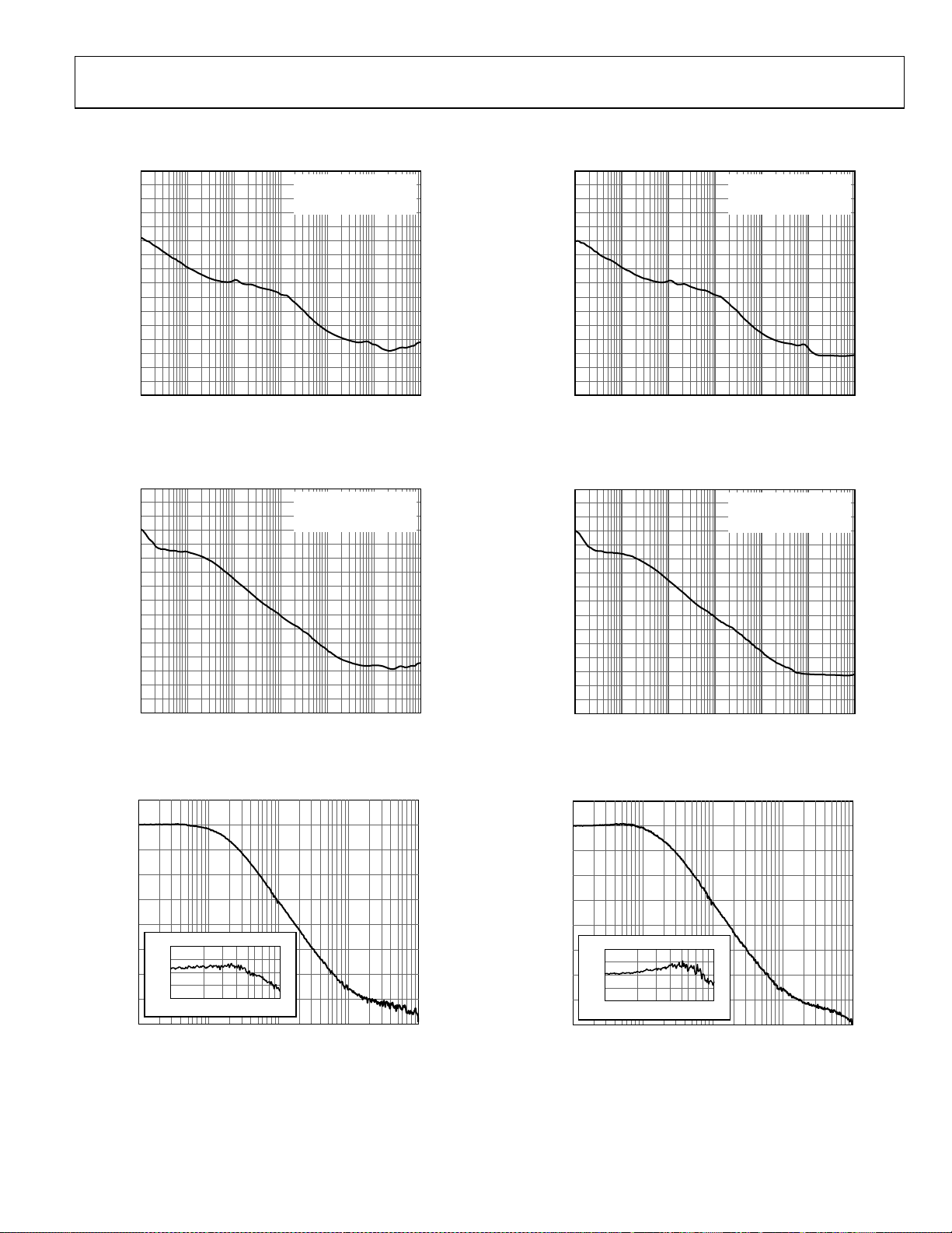
TYPICAL PERFORMANCE CHARACTERISTICS
–20
–30
–40
–50
–60
–70
–80
–90
–100
–110
–120
–130
PHASE NOISE (dBc/Hz)
–140
–150
–160
–170
–180
100 1k 10k 100k 1M 10M 100M
FREQUENCY OF FSET F ROM CARRIER (Hz)
CARRIER 622.080005MHz 0.8813dB
RMS JITTER:
0.827ps (12kHz TO 20MHz)
0.618ps (50kHz TO 80MHz)
Figure 4. Phase Noise, Fractional-N
= 622.08 MHz, f
(f
IN
= 622.08 MHz, f
OUT1
= 26 MHz)
XTAL
–20
–30
–40
–50
–60
–70
–80
–90
–100
–110
–120
–130
PHASE NOISE (dBc/Hz)
–140
–150
–160
4
07805-00
–170
–180
100 1k 10k 100k 1M 10M 100M
FREQUENCY OF FSET F ROM CARRIER (Hz)
Figure 7. Phase Noise, Integer-N
= 622.08 MHz, f
(f
IN
CARRIER 619.666689MHz 0.8705dB
RMS JITTER:
0.773ps (12kHz TO 20MHz)
0.559ps (50kHz TO 80MHz)
= 619.67 MHz, f
OUT1
= 26 MHz)
XTAL
07805-005
–20
–30
–40
–50
–60
–70
–80
–90
–100
–110
–120
–130
PHASE NOISE (dBc/Hz)
–140
–150
–160
–170
–180
100 1k 10k 100k 1M 10M 100M
FREQUENCY OF FSET F ROM CARRIER (Hz)
CARRIER 622.080027MHz 0.5414dB
RMS JITTER:
1.336ps (12kHz TO 20MHz)
0.463ps (50kHz TO 80MHz)
Figure 5. Phase Noise, 19.44 MHz Mode, Fractional-N
= 19.44 MHz, f
(f
IN
5
0
–5
–10
–15
–20
1.0
–25
0.5
JITTER TRANSFER (dB)
0
–30
–0.5
–1.0
–35
–40
10 100
10 100 1k 10k 100k
= 622.08 MHz, f
OUT1
FREQUENCY OFFSET (Hz)
= 52 MHz)
XTAL
Figure 6. Jitter Transfer (Minimal Peaking)
(Register 0x33[7] = 0)
–20
–30
–40
–50
–60
–70
–80
–90
–100
–110
–120
–130
PHASE NOISE (dBc/Hz)
–140
–150
–160
6
07805-00
–170
–180
100 1k 10k 100k 1M 10M 100M
FREQUENCY OF FSET F ROM CARRIER (Hz)
CARRIER 619.666712MHz 0.6233dB
RMS JITTER:
1.327ps (12kHz TO 20MHz)
0.438ps (50kHz TO 80MHz)
07805-007
Figure 8. Phase Noise, 19.44 MHz Mode, Integer-N
= 19.44 MHz, f
(f
IN
5
0
–5
–10
–15
–20
1.0
–25
0.5
JITTER TRANSFER (dB)
–30
0
–0.5
–35
–1.0
10 100
8
07805-00
–40
10 100 1k 10k 100k
= 619.67 MHz, f
OUT1
FREQUENCY OFFSET (Hz)
= 52 MHz)
XTAL
07805-009
Figure 9. Jitter Transfer (Nominal Peaking)
(Register 0x33[7] = 1)
Rev. B | Page 11 of
40
AD9551
35
25
30
25
20
15
SUPPLY CURRENT (mA)
10
5
100 1k
FREQUENCY (MHz)
LVPECL
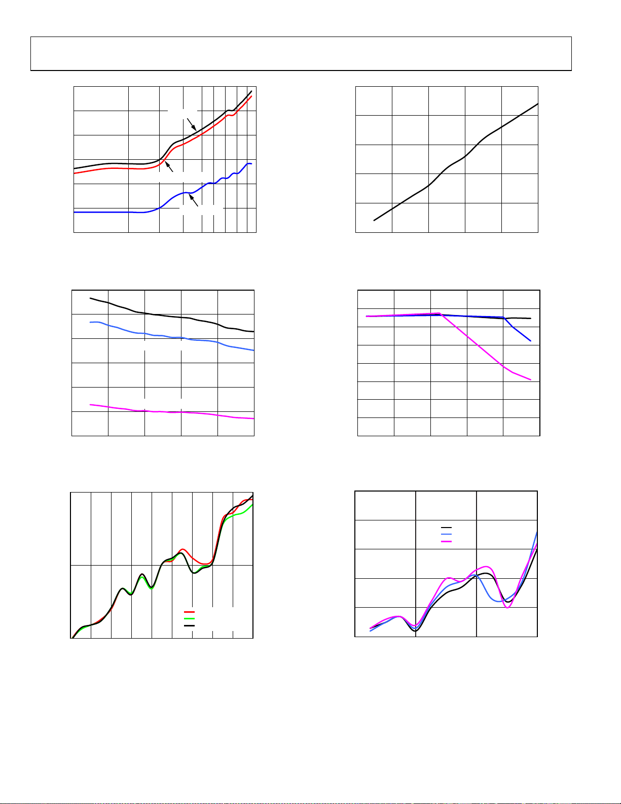
LVDS (STRONG)
LVDS (WEAK)
Figure 10. Supply Current vs. Output Frequency— LVPECL and LVDS
(10 pF Load)
1.6
1.4
1.2
1.0
0.8
AMPLITUDE (V p-p)
0.6
LVPECL
LVDS (STRONG)
LVDS (WEAK)
20
15
10
SUPPLY CURRENT (mA)
5
024
07805-
0
0 50 100 150 200 250
FREQUENCY (MHz )
07805-025
Figure 13 Supply Current vs. Output Frequency—CMOS
(10 pF Load)
4.0
3.5
3.0
2.5
2.0
1.5
AMPLITUDE (V p-p)
1.0
0.5
20pF
5pF
10pF
0.4
0 200 400 600 800 1000
FREQUENCY (MHz )
028
07805-
Figure 11. Peak-to-Peak Output Voltage vs. Frequency—LVPECL and LVDS
(10 pF Load)
60
55
DUTY CYCLE (%)
LVDS (WEAK)
LVDS (STRONG)
LVPECL
50
100 200 300 400 500 600 700 800 900 1000
FREQUENCY (MHz)
07805-026
Figure 12. Duty Cycle vs. Output Frequency—LVPECL and LVDS
(10 pF Load)
0
0 100 200 300 400 500
FREQUENCY (MHz)
Figure 14. Peak-to-Peak Output Voltage vs. Frequency—CMOS
55
54
53
52
DUTY CYCL E (%)
51
50
0 100 200 300
FREQUENCY (MHz )
5pF
10pF
20pF
Figure 15. Duty Cycle vs. Output Frequency—CMOS
07805-029
027
07805-
Rev. B | Page 12 of 40
AD9551
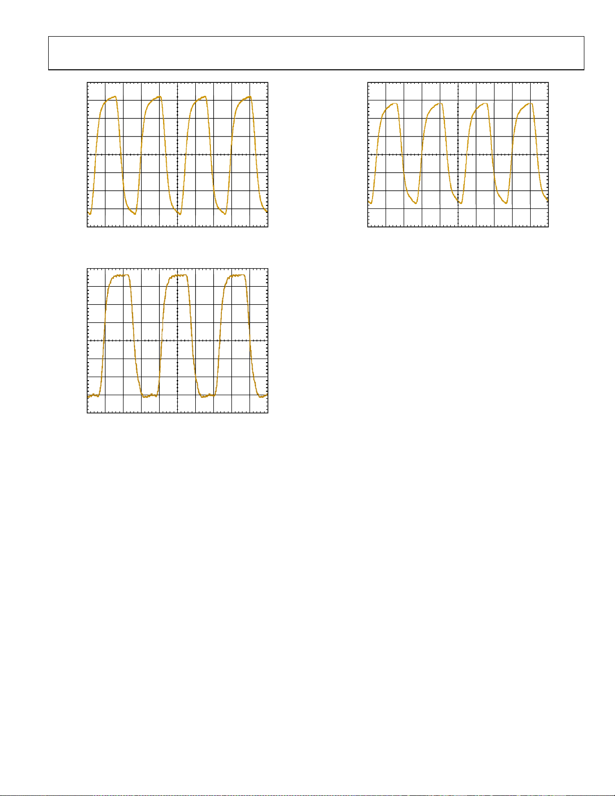
V
V
V
200mV/DI
007805-01
500ps/DIV
Figure 16. Typical Output Waveform—LVPECL
(805 MHz)
100mV/DI
500ps/DIV
Figure 18. Typical Output Waveform—LVDS
(805 MHz, 3.5 mA Drive Current)
07805-022
500mV/DI
1.25ns/DI V
07805-023
Figure 17. Typical Output Waveform—CMOS
(250 MHz, 10 pF Load)
Rev. B | Page 13 of 40

AD9551
(
)
PRESET FREQUENCY RATIOS
The frequency selection pins (A[3:0], B[3:0], and Y[3:0]) allow
the user to hardwire the device for preset input and output divider
values based on the pin logic states. The A[3:0] pins control the
REFA dividers, the B[3:0] pins control the REFB dividers, and
the Y[3:0] pins control the feedback and output dividers. The
pins decode ground or open connections as Logic 0 or Logic 1,
respectively. To override the preset divider settings, use the serial
I/O port to program the desired divider values.
Tabl e 13 lists the input divider values based on the logic state of
the frequency selection pins. The table headings are as follows:
• A[3:0], B[3:0]. The logic state of the A[3:0] or B[3:0] pins.
• N
, NB. The integer part of the REFA input divider (NA) or
A
the REFB input divider (N
).
B
• MOD
• FRAC
• f
, MODB. The modulus of the REFA input divider
A
SDM (MOD
divider SDM (FRAC
(FRAC
REF
, fREFB. The frequency of the REFA input (fREFA) or the
A
REFB input (f
) or the REFB input divider SDM (MODB).
A
, FRACB. The fractional part of the REFA input
A
) or the REFB input divider SDM
A
).
B
REF
).
B
The divider settings shown in Tab l e 13 cause the frequency at the
reference input of the output PLL’s PFD (f
) to operate at exactly
IF
26 MHz when using the indicated input reference frequency,
f
REF
or fREFB, assuming the use of a 26 MHz external crystal.
A
Table 13. Preset Input Settings
A[3:0], B[3:0] NA, NB MODA, MODB FRACA, FRACB fREFA, fREFB (MHz)
1
0000 23 130,000 110,800 622.08
0001 24 130,000 −120,000 625
0010 24 154,050 −114,594
0011 24 130,000 45,200
0100 24 166,400 96,400
0101 25 104,000 −44,625
0110 25 198,016 −42,891
0111 25 154,700 41,820
1000 25 154,050 74,970
1001 25 182,000 93,000
1010 25 153,400 108,120
1011 26 197,184 67,998
1100 26 146,900 83,612
1101 27 198,016 −161,755
1110 27 197,184 −115,995
2
1111
1
Assumes the use of a 26 MHz external crystal.
2
If all four A[3:0] pins or all four B[3:0] pins are Logic 1, the 19.44 MHz mode is in effect.
19.44 MHz mode
239
237
66
()
64
66
()
≡
64
75.10518
≡
16
239
75.10518
()
238
16
255
()
238
255
()
237
15
()
≈
14
255
()
236
()()
253
()
226
25575.10518
()
23816
25575.10518
()
23716
≈
52.64108.622
≡
53125.644625
421875.657
≈
≈
≈
64.669625
≈
66255
≈×
64237
≈
≈
≈
33.62708.622
18.660
51.66608.622
33.66908.622
16.67208.622
48
.693625
40.69608.622
38.704
35.707
Rev. B | Page 14 of 40
AD9551
(
(
(
(
(
(
(
(
()(
)
(
(
(
(
)
The Y[3:0] pins select the divider values for the feedback path of
the output PLL, as well as for the OUT1 dividers, P
OUT2 divider, P
, defaults to unity unless otherwise program-
2
and P1. The
0
med using the serial port. Tab l e 1 4 lists the feedback and output
divider values based on the logic state of the Y[3:0] frequency
selection pins. The table headings are as follows:
• Y[3:0]. The logic state of the Y[3:0] pins.
• N. The integer part of the feedback divider.
• MOD. The modulus of the feedback SDM.
• FRAC. The fractional part of the feedback SDM.
• P
, P1. The P0 and P1 divider values.
0
• f
. The frequency of the OUT1 output.
OUT1
Table 14. Preset Output Settings
Y[3:0] N MOD FRAC P0, P1 f
0000 143 520,000 289,600 6/1 622.08
0001 144 520,000 120,000 6/1 625
0010 144 308,100 236,736 6/1
0011 148 520,000 22,400 6/1
0100 148 465,920 343,840 6/1
0101 151 520,000 370,625 6/1
0110 152 465,920 163,160 6/1
0111 153 465,920 377,856 6/1
1000 154 328,640 151,168 6/1
1001 154 460,096 245,216 6/1
1010 155 490,880 56,192 6/1
1011 133 328,640 119,005 5/1
1100 133 470,080 433,856 5/1
1101 135 349,440 159,975 5/1
1110 136 394,368 11,577 5/1
1111 149 520,000 280,000 5/1
The divider settings shown in Tabl e 14 produce the indicated
frequency at OUT1 when the frequency at the reference input
of the output PLL’s PFD (f
) is exactly 26 MHz.
IF
When operating in the 19.44 MHz mode, the N, MOD, and FRAC
values may be different from those shown in Tab l e 14 , but the
f
values remain the same. The reason is that the 19.44 MHz
OUT1
mode relies on a crystal with a resonant frequency other than 26
MHz (see the 19.44 MHz Mode section in the Operating Modes
portion of the Theory of Operation section).
(MHz)
OUT1
239
)
33.62708.622
≈
237
66
)
≡
64
66
)
≡
64
75.10518
≡
16
2391675.10518
)
238
255
)
238
255
)
≈
237
15
)
≈
14
255
)
≈
236
66
255
64
237
253
)
226
2551675.10518
)
≈
238
2551675.10518
)
≈
237
10
8
52.64108.622
53125.644625
421875.657
18.660
≈
51.66608.622
≈
33.66908.622
64.669625
16.67208.622
48.693625
≈
40.69608.622
≈
38.704
35.707
6.77708.622
≡
Rev. B | Page 15 of 40

AD9551
THEORY OF OPERATION
OPERATING MODES
The AD9551 provides the following fundamental operating modes:
• Normal mode
• 19.44 MHz mode
Mode selection depends on the state of the frequency selection pins
(A[3:0] and B[3:0]). If all four of the A[3:0] pins or all four of
the B[3:0] pins are Logic 1s, the 19.44 MHz mode is in effect.
Otherwise, normal mode is in effect.
Normal Mode
Normal mode offers two methods of operation. The first method
relies on the frequency selection pins to configure the device.
The second method involves the use of the serial port for device
configuration.
The first method is for applications that use one of the input/output
frequency sets defined in Tabl e 13 and Ta bl e 1 4 (excluding the
19.44 MHz mode selection). The advantage of this method is
that the serial port is not required. Connect the pins to the appropriate logic levels, and the device operates with the defined input
and output frequencies. The pin settings establish all the necessary
internal divider values. Note, however, that this method requires an
external crystal with a resonant frequency of 26 MHz.
The second method, which relies on the serial port, enables the
user to program custom divider settings to achieve input/output
frequency ratios not available via the frequency selection pins.
Furthermore, the 26 MHz constraint on the external crystal no
longer applies. Note, however, that the external pin settings still
establish the default values of the dividers. The serial port simply
enables the user to override the default settings.
19.44 MHz Mode
This special operating mode allows for input references that
operate specifically at 19.44 MHz, 38.88 MHz, or 77.76 MHz.
The 19.44 MHz mode is invoked by the frequency selection pins
and occurs when either A[3:0] = 1111b or B[3:0] = 1111b. Furthermore, this mode requires an external crystal with one of the
following four possible resonant frequencies, based on the contents
of Register 0x33[5:4].
• 49.152 MHz
• 49.860 MHz
• 50.000 MHz
• 52.000 MHz
In the 19.44 MHz mode, the reference input dividers allow for
integer divide ratios of 1, 2, or 4 only, set via Register 0x1E[1:0].
Therefore, if f
if f
= 38.88 MHz, the divide ratio must be set to 2; and if fIN =
IN
77.76 MHz, the divide ration must be set to 4.
Note that for applications using both REFA and REFB in the
19.44 MHz mode, the input frequencies must match.
= 19.44 MHz, the divide ratio must be set to 1;
IN
Rev. B | Page 16 of 40
Although the 19.44 MHz mode limits the input divide ratio to
1, 2, or 4, the user has full control of the dividers in the output
section. This includes the integer and fractional components of
the output PLL feedback divider and the final output dividers
(P
, P1, and P2), enabling the synthesis of a wide range of output
0
frequencies.
Note that the 19.44 MHz mode alters the configuration of the input
PLL (see the Input PLL section).
When using the 19.44 MHz mode, the loop filter in the output PLL
requires a 100 nF capacitor. Furthermore, the user must program
the output PLL charge pump current to 25 µA (via Register 0x0A).
Note that SPI port programming capability is necessary when
using 19.44 MHz mode because it requires a charge pump current
that is different from the default value.
COMPONENT BLOCKS
Input Dividers
Each reference input feeds a dedicated reference divider block.
The input dividers provide division of the reference frequency
in integer steps from 1 to 63. They provide the bulk of the frequency prescaling necessary to reduce the reference frequency
to accommodate the bandwidth limitations of both the input
and output PLLs.
Input Sigma-Delta Modulators (SDM)
Each of the two input dividers is coupled with an optional, secondorder SDM, enabling fractional division of the input reference
frequency. With both integer and fractional divide capability, the
AD9551 can accept two different reference frequencies that span
a wide range of possible input frequency ratios.
A typical SDM offers fractional division in the form N + F/M,
where N is the integer part, M is the modulus, and F is the fractional part (F < M). All three parameters are positive integers. The
input SDMs of the AD9551 are atypical in that they implement
fractional division in the form, N + 1/2 + F/(2M), with F being
a signed integer, and |F| < M. Note that when the SDM is in use,
the minimum integer divide value is 4.
Both SDMs have an integrated pseudorandom binary sequence
(PRBS) generator. The PRBS generator serves to suppress spurious
artifacts by adding a random component to the SDM output. By
default, the PRBS generator is active in both input SDMs, but
the user can disable the PRBS using Register 0x1E[2].
Note that in 19.44 MHz mode, the input SDMs are inactive and
unavailable.
Reference Monitor
The reference monitor verifies the presence or absence of the
prescaled REFA and REFB signals (that is, after division by the
input dividers). The status of the reference monitor guides the
activity of the synchronization and switchover control logic.
Note that the DCXO must be operational for the reference
monitor to function.

AD9551
DLL A
REFA, REFA
÷
DELAY
HOLD A
10
A/B
HOLD A
HOLD B
OUT ENABLE
A/B
1
2
÷
0
DCXO HOLD
DELAY
REFB, REFB
REFERENCE
MONITOR
LOCKED
÷
Figure 19. Synchronization Block Diagram
Synchronization/Switchover Control
Figure 19, which is a block diagram of the hitless reference switchover circuit, shows that reference synchronization occurs after
the input reference dividers. The synchronization and switchover
functionality relies on the reference monitor logic to control the
operation of the three delay-locked loops (DLLs). The delay blocks
of the three DLLs are identical, so that they exhibit the same time
delay for a given delay value setting.
Note that the DCXO must be operational for the synchronization and switchover control to operate.
Both the REFA and REFB paths have a dedicated DLL (DLL A
and DLL B, respectively). DLL A and DLL B are each capable of
operating in either an open-loop or closed-loop mode under the
direction of the reference monitor status signals. When the
reference monitor selects one of the references as the active
reference, the DLL associated with the active reference operates
in open-loop mode. While in open-loop mode, the DLL delays
the active reference by a constant time interval based on a fixed
delay value. As long as one of the references is the active reference, the other reference is, by default, the alternate reference.
The DLL associated with the alternate reference operates in closedloop mode. While in closed-loop mode, the DLL automatically
adjusts its delay so that the rising edge of the delayed alternate
reference is edge-aligned with the rising edge of the delayed
active reference.
10
A/B
ACC
REF.
DLL
LOCKED
ACC
A/B
HOLD B
DLL B
P
F
D
P
F
D
DQ
OUT ENABLE
N/2
OUT ENABLE
1
0
A/B
INPUT
PLL
DCXO
TO
OUTPUT
PLL
DCXO HOLD
When the reference monitor selects one of the references as the
active reference, it switches the output mux to select the output of
the DLL associated with the active reference and, simultaneously,
routes the active reference to the reference DLL. The reference
DLL automatically measures the period of the active reference
(with approximately 250 ps accuracy). When the reference DLL
locks, the value of its delay setting (N) represents one period of
the active reference. Upon acquiring lock, the reference DLL
captures N and divides it by two (N/2 corresponds to a delay value
that represents a half-cycle of the active reference). Both DLL A and
DLL B have access to the N/2 value generated by the reference DLL.
The following paragraphs describe the typical sequence of events
resulting from a device reset, power-up, or return from holdover mode.
Active Reference and Alternate Reference
The reference monitor continuously checks for the presence of the
divided REFA and/or REFB signals. If both signals are avail-able,
the device arbitrarily selects one of them as the active reference,
making the other the alternate reference. If only one of the
references is available, it becomes the active reference, making the
other the alternate reference (if it ever becomes available). In
either case, the following two events occur:
• The output mux selects the output of the active DLL as the
source to the input PLL.
• The input mux selects the active reference as the source to
the reference DLL.
07805-011
Rev. B | Page 17 of 40

AD9551
The reference DLL measures the period of the active reference
and produces the required N/2 delay value. When the reference
DLL locks, the following three events occur:
• Both DLL A and DLL B are enabled.
• The DLL associated with the active reference enters open-
loop mode.
• The DLL associated with the alternate reference enters
closed-loop mode.
This implies that the signal driving the input PLL is the active
reference (after division by its input divider) with a half-cycle delay.
Because the alternate DLL is in closed-loop mode, and assuming
that the alternate reference is available, the output of the alternate
DLL is edge-aligned with the delayed output of the active DLL.
Furthermore, the closed-loop operation of the alternate DLL
causes its delay value to be adjusted dynamically so that it maintains nominal edge alignment with the output of the active DLL.
Edge alignment of the active and alternate references is the key
to the hitless switchover capability of the AD9551.
Reference Switchover and Holdover Mode
If the reference monitor detects the loss of the active reference,
it initiates the following three simultaneous operations:
• The output mux selects the output of the alternate DLL.
• The alternate DLL holds its most recent delay setting (that
is, the delay setting that edge-aligned the output of the alternate DLL with the output of the active DLL). Note that this
operation ensures hitless switching between references.
• The new active reference is connected to the reference DLL
to measure its period (that is, a new N/2 value).
Because the failed alternate reference is assigned to the alternate
DLL, upon its return the alternate DLL (which is in closed-loop
mode) automatically edge-aligns the delayed alternate reference
with the delayed active reference. Thus, if the new active reference
fails, switchover to the alternate reference occurs in a hitless
manner. This method of swapping the functionality of DLL A
and DLL B as either active (open-loop) or alternate (closed-loop)
allows for continuous hitless switching from one reference to
the other, as needed (assuming the availability of an alternate
reference upon failure of the active reference).
Note that if both references fail, the device enters holdover
mode. In this case, the reference monitor holds the DCXO at its
last setting prior to the holdover condition, and the DCXO free
runs at this setting until the holdover condition expires.
Forcing Selection of the Active Reference
Because the synchronization mechanism autonomously switches
between references, the user has no way of knowing which
reference is currently the active reference. However, the device
can be forced to select a specific input reference as the active
reference. For example, to force REFA to be the active reference,
power down the REFB input receiver by programming the appropriate registers (or disconnect the REFB signal source).
The absence of a REFB signal causes the device to perform
a hitless switchover to REFA. If REFA is already the active
reference, the absence of REFB results in no action, and REFA
remains the active reference. In this way, the user can ensure
that REFA is the active reference. Likewise, by using the same
procedure but reversing the roles of the two references, the user
can force the device to select REFB as the active reference.
Digitally Controlled Crystal Oscillator (DCXO)
The DCXO is the fundamental building block of the input PLL
(see the Input PLL section). The DCXO relies on an external
crystal (19.44 MHz to 52 MHz) as its frequency source. The
resonant frequency of the external crystal varies as a function
of the applied load capacitance. The AD9551 has two internal
capacitor banks (static and dynamic) that provide the required
load capacitance. In operation, the control loop of the input PLL
automatically adjusts the value of the capacitive load to push or
pull the crystal resonant frequency over a small range of approximately ±50 ppm.
The tuning capacitor bank sets the static load capacitance, which
defaults to ~2 pF. The varactor bank is a dynamic capacitance
controlled by the DCXO to push or pull the crystal resonant
frequency. The nominal varactor capacitance is ~6 pF, and
when combined with the 2 pF static capacitance and 2 pF of
typical parasitic capacitance, the total crystal load capacitance is
~10 pF (default).
The user can alter the default load capacitance by changing
the static load capacitance of the tuning capacitor bank via
Register 0x1B[5:0]. These six bits set the static load capacitance
in 0.25 pF increments up to a maximum of ~16 pF.
The control loop of the input PLL locks the DCXO to the active
reference signal by dynamically controlling the varactor capacitance. Note that the narrow frequency control range (±50 ppm) of
the varactor bank, combined with the default operating parameters
of the AD9551, dictate the use of a crystal with specified load
capacitance of 10 pF and a frequency tolerance of 20 ppm (see
the NDK NX3225SA, for example).
The narrow tuning range of the DCXO has two implications.
First, the user must properly choose the divide ratio of the input
reference divider to establish a frequency that is within the DCXO
tuning range. Second, the user must ensure that the jitter/wander
of the input reference is low enough to ensure the stability of the
input PLL control loop for applications where the DCXO is the
reference source for the output PLL (the default configuration).
Normally, the input SDMs help to mitigate the input jitter because
of the way they interact with the behavior of the input PLL. Input
jitter becomes an issue, however, when the input dividers operate
in integer-only mode or the input PLL is bypassed.
Rev. B | Page 18 of 40

AD9551
Input PLL
The input PLL consists of a phase/frequency detector (PFD),
a digital loop filter, and a digitally controlled crystal oscillator
(DCXO) that operates in a closed loop. The loop contains a 2×
frequency multiplier, a 2× frequency divider, a 5× divider that
has a dedicated SDM, and switching logic, as shown in Figure 20.
XTAL
2
÷
2x
SDM
÷
1
0
5
f
REF
P
F
D
LOOP
FILTER
DIG.
19.44MHz MODE
DCXO
1
0
Figure 20. Input PLL
19.44MHz MODE
REG. 0x33[6]
0
1
REG. 0x1D[2]
TO
OUTPUT
PLL
07805-012
The input PLL has a digital loop filter with a loop bandwidth of
approximately 180 Hz. This relatively narrow loop bandwidth
gives the AD9551 the ability to suppress jitter appearing on the
input references (REFA and REFB). By default, the sample rate
of the digital loop filter is f
REF
/8 (f
is the frequency of the active
REF
input reference after it is scaled down by the input divider). This
yields a loop response with peaking of typically <0.2 dB. For applications that can benefit from a reduced acquisition time but can
tolerate more peaking (~0.5 dB), the user can increase the sample
rate of the loop filter to f
via Register 0x33[7].
REF
The configuration of the input PLL depends on the state of the
frequency selection pins, which establishes whether the device
operates in the normal mode or the 19.44 MHz mode. The configuration of the input PLL also depends on the state of the 2×
frequency multiplier bit (Register 0x1D[2]) and the state of the
2× frequency divider bit (Register 0x33[6]).
With the device in normal mode, the input PLL feedback signal
and the signal delivered to the output PLL are the same. In this
mode, the user has three options to scale the frequency at the
output of the DCXO.
• Unity (default). The crystal frequency is the same as f
• Frequency upconversion using the 2× multiplier: f
REF
REF
.
is
twice the crystal frequency
• Frequency downconversion using the 2× divider: f
REF
is
half the crystal frequency.
To select the upconversion option, set Register 0x1D[2] to 1. To
select the downconversion option, set Register 0x33[6] to 1.
Note that setting Register 0x1D[2] to 1 renders Register 0x33[6]
ineffective (see Figure 20).
In all cases mentioned previously, the user must ensure that f
meets the required relationship relative to the crystal resonant
frequency. This is important because the narrow control range of
the DCXO requires close adherence to the required frequency
ratio (1/2, 1, or 2, depending on the selected option). Note, also,
that the frequency delivered to the output PLL is always the
same as f
in normal mode.
REF
When the device is in 19.44 MHz mode, the user must ensure
that f
= 19.44 MHz. In 19.44 MHz mode, the configuration of
REF
the input PLL is different from that of normal mode. Specifically,
the feed-back signal and the signal delivered to the output PLL
are no longer the same. Instead, the device automatically configures
the feedback path to include the 2× frequency multiplier along
with a 5× divider coupled to a dedicated third-order SDM. The
device automatically sets the modulus of this SDM based on the
crystal frequency configured by Register 0x33[5:4]. This SDM also
has a built-in PRBS generator to randomize its output sequence.
Even though the device automatically configures the feedback
path in 19.44 MHz mode, the user can select the 2× multiplied or
2× divided output of the DCXO as the signal to the output PLL.
The 2× divider is in effect when Register 0x1D[2] = 0 (default).
The 2× multiplier is in effect when Register 0x1D[2] = 1. Note
that, unlike normal mode, the 19.44 MHz mode does not have
a unity option.
Using Register 0x1D[1] allows the user to bypass the entire input
PLL section. With the input PLL bypassed, the prescaled active
input reference signal (after synchronization) routes directly to the
PFD of the output PLL. However, even when the input PLL is
bypassed, the user must provide an external crystal so that the
DCXO is functional because the reference monitor and reference
synchronization blocks use the DCXO output as a clock source.
Output PLL
The output PLL consists of a phase-frequency detector (PFD),
a partially integrated analog loop filter (Figure 21), an integrated
voltage-controlled oscillator (VCO), and a feedback divider
with an optional third-order SDM that allows for fractional
divide ratios. The output PLL produces a nominal 3.7 GHz signal
that is phase-locked to the prescaled active input reference signal.
The PFD of the output PLL drives a charge pump that increases,
decreases, or holds constant the charge stored on the loop filter
capacitors (both internal and external). The stored charge results in
a voltage that sets the output frequency of the VCO. The feedback
loop of the PLL causes the VCO control voltage to vary in such
a way as to phase lock the PFD input signals.
FROM
CHARGE
PUMP
2.5kΩ
17
EXTERNAL
LOOP FILTER
CAPACITOR
1.25kΩ 1.25kΩ 2.5kΩ
105pF 15p F 15pF 20pF
Figure 21. Internal Loop Filter
REF
TO
VCO
07805-013
Rev. B | Page 19 of 40

AD9551
The gain of the output PLL is proportional to the current
delivered by the charge pump. The user can override the default
charge pump current setting, and, thereby, the PLL gain, by using
Register 0x0A[7:0].
The output PLL has a VCO with 128 frequency bands spanning
a range of 3350 MHz to 4050 MHz (3700 MHz nominal). However, the actual operating frequency within a particular band
depends on the control voltage that appears on the loop filter
capacitor. The control voltage causes the VCO output frequency
to vary linearly within the selected band. This frequency variability allows the control loop of the output PLL to synchronize
the VCO output signal with the reference signal applied to the
PFD. Typically, the device selects the appropriate band and adjusts
the signal level as part of its calibration process. However, the
user can force calibration by first enabling SPI control of VCO
calibration (Register 0x0E[2] = 1) and then writing a 1 to the
calibrate VCO bit (Register 0x0E[7]). To facilitate system debugging, the user can override the VCO band setting by first
enabling SPI control of the VCO band (Register 0x0E[0] = 1)
and then writing the desired value to Register 0x10[7:1].
The output PLL has a feedback divider coupled with a third-order
SDM (similar to the REFA and REFB input dividers) that enables
the output PLL to provide integer-plus-fractional frequency upconversion. The integer factor, N, is variable from 0 to 255 via an
8-bit programming register. However, the minimum practical value
of N is 64 because this sufficiently reduces the VCO frequency
in the PLL feedback path to an acceptable range. The SDM in the
feedback path allows for a fractional divide value that takes the
form of N + F/M, where N is the integer part (eight bits), M is
the modulus (20 bits), and F is the fractional part (20 bits), with
all three parameters being positive integers. The feedback SDM
gives the AD9551 the ability to support a wide range of output
frequencies with exact frequency ratios relative to the input
reference.
PLL Locked Indicators
Both the input and output PLLs provide a status indicator that
appears at an external pin. The indicator shows when the PLL has
acquired a locked condition. The input PLL provides the INPUT
PLL LOCKED signal, and the output PLL provides the OUTPUT
PLL LOCKED signal.
Output Dividers
Three integer dividers exist in the output chain. The first divider
) yields an integer submultiple of the VCO frequency. The
(P
0
second divider (P
integer submultiple of the output frequency of the P
The third divider (P
) establishes the frequency at OUT1 as an
1
divider.
0
) establishes the output frequency at OUT2
2
as an integer submultiple of the OUT1 frequency.
Output Drivers
The user has control over the following output driver parameters
via the programming registers:
• Logic family and pin functionality
• Polarity (for CMOS family only)
• Drive current
• Power-down
The logic families are LVDS, LVPECL, and CMOS. Selection of
the logic family is via the mode control bits in the OUT1 driver
control register (Register 0x32[5:3]) and the OUT2 driver control
register (Register 0x34[5:3]), as detailed in Tab l e 1 5 . Regardless
of the selected logic family, each output driver uses two pins: OUT1
and
OUT1
are used by one driver, and OUT2 and
OUT2
are used
by the other. This enables support of the differential signals
associated with the LVDS and LVPECL logic families. CMOS,
on the other hand, is a single-ended signal requiring only one
output pin, but both output pins are available for optional provision of a dual, single-ended CMOS output clock. Refer to the first
entry (CMOS (both pins)) in . Table 15
Table 15. Output Channel Logic Family and Pin Functionality
Mode
Control Bits[2:0] Logic Family and Pin Functionality
000 CMOS (both pins)
001 CMOS (positive pin), tristate (negative pin)
010 Tristate (positive pin), CMOS (negative pin)
011 Tristate (both pins)
100 LVDS
101 LVPECL
110 Undefined
111 Undefined
If the mode bits indicate the CMOS logic family, the user has
control of the logic polarity associated with each CMOS output
pin via the OUT1 and OUT2 driver control registers.
If the mode bits indicate the CMOS or LVDS logic family, the
user can select whether the output driver uses weak or strong
drive capability via the OUT1 and OUT2 driver control registers.
In the case of the CMOS family, the strong setting allows for
driving increased capacitive loads. In the case of the LVDS family,
the nominal weak and strong drive currents are 3.5 mA and
7 mA, respectively.
The OUT1 and OUT2 driver control registers also have a powerdown bit to enable/disable the output drivers. The power-down
function is independent of the logic family selection.
Note that, unless the user programs the device to allow SPI port
control of the output drivers, the drivers default to LVPECL or
LVDS, depending on the logic level on the OUTSEL pin (Pin 16).
For OUTSEL = 0, both outputs are LVDS. For OUTSEL = 1, both
outputs are LVPECL. In the pin-selected LVDS mode, the user
can still control the drive strength, using the SPI port.
Rev. B | Page 20 of 40

AD9551
{
}
∈
{
}
∈
{
}
∈
−
−
{
}
∈
{
∈
{
}
∈
{
∈
{
}
∈
{
}
∈
{
}
∈
HOLDOVER MODE
In the absence of both input references, the device enters holdover
mode. Holdover is a secondary function that is provided by the
input PLL. Because the DCXO has an external crystal as its frequency source, it continues to operate in the absence of the input
reference signals. When the device switches to holdover, the DCXO
is held at the frequency at which it was operating just prior to
switchover. The device continues operating in this mode until
a reference signal becomes available; the device then exits holdover
mode, and the input PLL resynchronizes with the active reference.
JITTER TOLERANCE
Jitter tolerance is the ability of the AD9551 to maintain lock in the
presence of sinusoidal jitter. The AD9551 meets the DS1 reference
input jitter tolerance mask per Telcordia GR-1244-CORE (see
Figure 22). The acceptable jitter tolerance is the region above the
mask.
10
1
JITTER (UI p-p)
EXTERNAL TI MING MASK
0.1
10 100 1k 10k 100k
JITTER F REQUENCY (Hz)
Figure 22. Jitter Tolerance
LINE TIMING MASK
07805-031
EXTERNAL LOOP FILTER CAPACITOR
The output PLL loop filter requires the connection of an external
capacitor from LF (Pin 17) to LDO_VCO (Pin 22). The value of
the external capacitor depends on the operating mode (normal
or 19.44 MHz). Normal mode requires a 12 nF capacitor that sets
the loop bandwidth at approximately 70 kHz and ensures loop
stability over the intended operating parameters of the device.
The 19.44 MHz mode requires a 100 nF capacitor, along with
a change in the output PLL charge pump current to 25 µA, via
Register 0x0A. This establishes similar loop bandwidth and
stability criteria as found in normal mode.
Note that the 19.44 MHz mode does not function properly
unless the user changes the output PLL charge pump current
from its default setting to 25 A.
OUTPUT/INPUT FREQUENCY RELATIONSHIP
Following are the three equations that define the frequency
at OUT1 and OUT2 (f
OUT1
and f
in the equations throughout this datasheet, the subscripted x
indicates A or B.
, respectively). Note that
OUT2
⎛
⎜
=
⎜
REFIF
x
⎜
N
x
⎜
⎝
⎜
ff
K
⎛
FRAC
1
⎜
++
⎜
⎝
MOD
FRAC
OUT1
⎛
N
⎜
ff
=
IF
⎜
⎝
⎞
+
MOD
⎟
2)
⎟
PP
10
⎠
f
f =
OUT2
OUT1
3)
P
2
where:
f
REF
and fREFB are the input reference frequency, with the
A
subscripted A or B indicating REFA or REFB, respectively.
f
is the frequency at the input of the output PLL’s PDF.
IF
and P1 are OUT1 divider values.
P
0
P
is the OUT2 divider value.
2
K is the input mode scale factor.
N
, NB, FRACA, FRACB, MODA, and MODB are the input reference
A
divider values, with the A or B subscript indicating REFA or REFB,
respectively.
N, FRAC, and MOD are the feedback divider values for the
output PLL.
The various dividers have the following constraints:
N 63,,2,1 L with SDM disabled
x
N 63,,4,3 L with SDM active
x
FRAC
x
MOD 287,524,,2,1 L
x
}
255,,65,64 LN
FRAC 575,048,1,,1,0 L
}
575,048,1,,2,1 LMOD
P 11,,5,4 L
0
P 63,,2,1 L
1
P 63,,2,1 L
2
The VCO imposes the following constraint on f
3350
FRAC
+
MOD
⎞
⎟
MHz
⎟
⎠
⎛
⎜
⎜
N
⎝
The input frequencies (f
⎛
4050
⎜
≤≤
f
IF
⎜
+
N
⎝
REF
and fREFB) must satisfy the following
A
relationship:
f
REF
FRAC
⎜
N
++
A
⎜
⎝
MOD
=
⎞⎛
A
⎟
N
B
⎟
A
⎠
287,524,,287,524,288,524 L
FRAC
MOD
⎜
⎜
⎝
⎞
⎟
⎟
1)
⎟
⎞
⎟
x
⎟
⎟
⎟
)(22
x
⎠
⎠
:
IF
⎞
⎟
MHz
⎟
⎠
f
REF
BA
FRAC
11
++
MOD
22)(22
⎞⎛
B
⎟
⎟
)(
B
⎠
Rev. B | Page 21 of 40

AD9551
The value of K depends on the device configuration, as shown
in Tabl e 16 .
Table 16. Configuring the Value of K
Mode f
K Description
CRYSTAL
19.44 MHz 52 MHz 1300/243 Using 2× multiplier
325/243 Using 2× divider
50 MHz 1250/243 Using 2× multiplier
625/486 Using 2× divider
49.86 MHz 277/54 Using 2× multiplier
277/216 Using 2× divider
49.152 MHz 2048/405 Using 2× multiplier
512/405 Using 2× divider
Normal 1 Crystal independent
The user must carefully consider the operating frequency of the
externally connected crystal resonator (assuming that the input
PLL is not bypassed). Because the DCXO is capable of pulling
the crystal over a 50 ppm range only, the output frequency of
the DCXO is essentially identical to the crystal frequency.
The denominator of Equation 1 is the input division factor, which
has an integer part (N
) due to an integer divider, as well as an
x
optional fractional part that is associated with the input SDM.
1/2 + FRAC
/(2 × MODx)
x
Note that when bypassing the SDM, the device forces the fractional part to 0 (equivalent to FRAC
= −MODx).
x
The numerator of Equation 2 contains the feedback division
factor, which has an integer part (N) due to an integer divider,
as well as an optional fractional part (FRAC/MOD) that is
associated with the feedback SDM.
Equation 1 and Equation 2, along with the constraints placed on
their variables, imply a rational relationship between f
That is, the ratio f
must be expressible as a ratio of two
OUT1/fREF
REF
and f
OUT1
.
integers. For example, it is not possible to configure the device
to satisfy a frequency ratio having a value of −2 because it is
irrational (that is, not expressible as a ratio of two integers).
CALCULATING DIVIDER VALUES
This section provides a 5-step procedure for calculating the divider
values when given a specific f
OUT1/fREF
described in general terms, but a specific example is provided
for clarity. The example assumes the use of the frequency control
pins with A[3:0] = 0010 and Y[3:0] = 0100 (see Table 13 and
Tabl e 14 ). The example parameters are as follows:
239
⎞
⎛
REF
08.622
=f
⎜
⎝
237
⎟
⎠
MHz
ratio. The methodology is
Calculation Steps
1. Ensure that f
As shown in the following equation, f
as a ratio of two integers, so f
f
OUT1
=
f
REF
Determine the output divide factor (ODF).
2.
Note that the VCO frequency (f
4050 MHz. The ratio, f
Given the specified value of f
range of f
and f
OUT1
66
⎛
625
⎜
64
⎝
⎛
08.622
⎜
237
⎝
, the ODF spans a range of 5.2 to 6.3. The ODF
VCO
are rationally related.
REF
OUT1
⎞
⎟
⎠
239
⎞
⎟
⎠
VCO/fOUT1
OUT1
is expressible
OUT1/fREF
and f
are rationally related.
REF
,977
)100)(237)(66(625
==
)64)(239(62208
) spans 3350 MHz to
VCO
, indicates the required ODF.
(~644.53 MHz) and the
must be an integer, which means that ODF = 6 (because 6
is the only integer between 5.2 and 6.3).
Determine suitable values for P
3.
and P1.
0
The ODF is the product of the two output dividers; that is,
ODF = P
for the given example. Therefore, we have P
constraints that P
× P1. It has already been determined that ODF = 6
0
× P1 = 6, with the
0
and P1 are both integers and that 4 ≤ P0 ≤ 11
0
(see the Output/Input Frequency Relationship section).
These constraints lead to the singular solution of P
= 6, and P1
0
= 1.
Although this particular example yields a singular solution
for the output divider values with f
frequencies result in multiple ODFs rather than just
f
OUT1
one. For example, if f
= 100 MHz, the ODF ranges from
OUT1
≈ 644.53 MHz, some
OUT1
34 to 40. This leads to an assortment of possible values for
and P1, as shown in Tabl e 17 .
P
0
The P
and P1 combinations listed in Tabl e 17 are all equally
0
valid. However, note that they yield only three valid ODF
values (35, 36, and 40) from the original range of 34 to 40.
Table 17. Combinations of P0 and P1
P0 P
ODF
1
4 9 36
4 10 40
5 7
5 8
6 6
7 5
8 5
9 4
35
40
36
35
40
36
10 4 40
000,625
568553,951
,
f
OUT1
f
IF
66
⎞
⎛
625
=
MHz26=
MHz
⎟
⎜
64
⎠
⎝
Rev. B | Page 22 of 40

AD9551
N
f
4. Determine the feedback divider values for the output PLL.
Repeat this step for each ODF when multiple ODFs exist
(for example, 35, 36, and 40, in the case of Tabl e 17 ).
To calculate the feedback divider values for a given ODF, use
the following equation:
⎞
⎛
f
OUT1
⎟
⎜
⎟
⎜
f
IF
⎠
⎝
ODF
X
=×
Y
Note that the left side of the equation contains variables
with known quantities. Furthermore, the values are necessarily rational, so the left side is expressible as a ratio of two
integers, X and Y. The following is an example equation:
66
26
⎞
⎡
⎟
64
⎥⎤⎢
⎦⎣
⎟
6
⎟
⎟
⎠
)6)(66(625
1664
)64(26
X
500,247
===×
Y
⎛
⎜
⎜
⎜
⎜
⎝
625
In the context of the AD9551, X/Y is always an improper
fraction. Therefore, it is expressible as the sum of an integer,
N, and the proper fraction, R/Y (R and Y are integers).
N
R
+=
Y
X
Y
500,247
1664
R
N +=
Y
Therefore, the example yields N = 148, Y = 1664, and R =
1228. To arrive at this result, use long division to convert the
improper fraction, X/Y, to an integer (N) and a proper fraction
(R/Y). Note that dividing Y into X by means of long division
yields an integer, N, and a remainder, R. The proper fraction
has a numerator (R, the remainder) and a denominator (Y,
the divisor), as follows:
YX
–NY
R
Figure 23. Example Long Division
Y
X
= N +
R
Y
07805-030
It is imperative to use long division to obtain the correct
results. Avoid the use of a calculator or math program
because these do not always yield correct results due to
internal rounding and/or truncation. Some calculators or
math programs may be up to the task if they can handle very
large integer operations, but such are not common.
In the example, N = 148 and R/Y = 1228/1664, which reduces
to R/Y = 307/416. These values of N, R, and Y constitute
the fol-lowing respective feedback divider values: N = 148,
FRAC = 307, and MOD = 416.
The only caveat is that N and MOD must meet the constraints
given in the Output/Input Frequency Relationship section.
In the example, FRAC is nonzero, so the division value is
an integer plus the fractional component, FRAC/MOD. This
implies that the feedback SDM is necessary as part of the feedback divider. If FRAC = 0, the feedback division factor is an
integer and the SDM is not required (it can be bypassed).
Although the feedback divider values obtained in this way
provide the proper feedback divide ratio to synthesize the
exact output frequency, they may not yield optimal jitter
performance at the final output. One reason for this is that
the value of MOD defines the period of the SDM, which has
a direct impact on the spurious output of the SDM. Specifically, the SDM spectrum has MOD at evenly spaced
spurs between dc and f
. Thus, the spectral sepa-ration
IF
(f) of the spurs associated with the feedback SDM is
IF
MOD
=Δ
f
Because the SDM is in the feedback path of the output PLL,
these spurs appear in the output signal as spurious components offset by f from f
. Therefore, a small MOD value
OUT1
produces relatively large spurs, with relatively large frequency
offsets from f
smaller spurs but more closely spaced to f
, whereas a large MOD value produces
OUT1
. Clearly, the
OUT1
value of MOD has a direct impact on the spurious content
(that is, jitter) at OUT1.
Generally, the largest possible MOD value yields the smallest
spurs. Thus, it is desirable to scale MOD and FRAC by the
integer part of 2
20
divided by the value of MOD obtained
previously. In the example, the value of MOD is 416, yielding
a scale factor of 2520 (the integer part of 2
20
/416). A scale
factor of 2520 leads to FRAC = 307 × 2520 = 773,640, and
MOD = 416 × 2520 = 1,048,320.
However, these FRAC and MOD values are different from
those that appear in Tabl e 14 (Y[3:0] = 0100). The reason is
that a scale factor of 1120 (instead of 2520) was found to yield
the most accept-able overall performance. A scale factor of
1120 results in the following Tab le 1 4 values: FRAC =
343,840 and MOD = 465,920.
5.
Determine the values of the REFA (or REFB) input dividers.
To calculate the feedback divider values, use the following
equation:
f
X
REF
=
Y
f
IF
Note that the left side of the equation contains variables
with known quantities. Furthermore, the values are necessarily rational, so the left side is expressible as a ratio of two
integers, X and Y. The following is an example equation:
239
⎞
⎛
08.622
⎟
26
⎜
237
⎠
⎝
)239(62208
)237)(26(100
200,616
X
712,867,14
===
Y
Rev. B | Page 23 of 40

AD9551
As in Step 4, use long division to convert the fraction, X/Y
to an integer, N, and a proper fraction, R/Y (R and Y a
integers). The same caution giv
en in Step 4 applies here,
re
regarding the need to use long division rather than a
calculator or a math program.
Given the example of X = 14,867,712 and Y = 616,200,
long division yields the following: N = 24 and R/Y =
78,912/616,200, which reduces to R/Y = 3,288/25,675. The
only caveats are that N must meet t
and N
given in the Output/Input Frequency R
B
hat Y < 2
19
(524,288). section and t
he constraints for N
elationship
A
Next, use R and Y to compute the following:
Q = 2R − Y
Using R = 3288 and Y = 25,675 from
the previous example
yields
Q = 2 × 3288 − 25,675 = −19,099
These va
divider values: N
lues of N, Q, and Y constitute the respective input
= 24, FRACx = −19,099, and MODx =
x
25,675.
In the example, FRAC
an integer plus the fractional component, FRAC
is nonzero, so the division value i
x
/MODx.
x
This implies that the input SDM is necessary as part of the
input divider. If FRAC
= 0, then the input division factor is
x
an integer and the SDM is not required (it can be bypassed).
,
s
The choice of MOD
affects the jitter performance of the
x
input section in a manner similar to the feedback dividers.
However, the spectral spacing of the spurs for the input
SDMs is as follows:
f
REF
f
=Δ
x
()( )
x
12
FRACNMOD
++×
xxx
The input SDMs are similar to the feedback SDM in that it
is desirable to scale MOD
19
2
, divided by the value of MODx that was calculated pre-
and FRACx by the integer part of
x
viously in Step 5. In the example calculation, the value of
is 25,675, which leads to a scale factor of 20 (the integer
MOD
x
part of 2
results: FRAC
19
/25,675). A scale factor of 20 yields the following
= −19,099 × 20 = −381,980 and MODx =
x
25,675×20 = 513,500.
However, these FRAC
and MODx values are different from
x
those that appear in Tabl e 13 (A[3:0] = 0010). The reason is
that a scale factor of 6 (instead of 20) was found to yield the
most acceptable overall performance. A scale factor of 6
results in the following Tab le 1 3 values: FRAC
6 = −114,594, and MOD
= 25,675 × 6 = 154,050.
x
= −19,099 ×
x
LOW DROPOUT (LDO) REGULATORS
The AD9551 is powered from a single 3.3 V supply and contains
on-chip LDO regulators for each function to eliminate the need
for external LDOs. To ensure optimal performance, each LDO
output should have a 0.47 F capacitor connected between its
access pin and ground.
Note that for best performance, the LDO bypass capacitors
must be placed in close proximity to the device.
Rev. B | Page 24 of 40

AD9551
APPLICATIONS INFORMATION
THERMAL PERFORMANCE
Table 18. Thermal Parameters for the 40-Lead LFCSP Package
Symbol Thermal Characteristic Using a JEDEC51-7 Plus JEDEC51-5 2S2P Test Board
1
Value2Unit
θJA Junction-to-ambient thermal resistance, 0.0 m/sec airflow per JEDEC JESD51-2 (still air) 45 °C/W
θ
Junction-to-ambient thermal resistance, 1.0 m/sec airflow per JEDEC JESD51-6 (moving air) 40 °C/W
JMA
θ
Junction-to-ambient thermal resistance, 2.5 m/sec airflow per JEDEC JESD51-6 (moving air) 36 °C/W
JMA
θJB Junction-to-board thermal resistance, 1.0 m/sec airflow per JEDEC JESD51-8 (moving air) 28 °C/W
θJC Junction-to-case thermal resistance (die-to-heat sink) per MIL-Std 883, Method 1012.1 8 °C/W
ΨJT Junction-to-top-of-package characterization parameter, 0 m/sec airflow per JEDEC JESD51-2 (still air) 0.6 °C/W
1
The exposed pad on the bottom of the package must be soldered to ground to achieve the specified thermal performance.
2
Results are from simulations. The PCB is a JEDEC multilayer type. Thermal performance for actual applications requires careful inspection of the conditions in the
application to determine if they are similar to those assumed in these calculations.
The AD9551 is specified for a case temperature (T
ensure that T
is not exceeded, an airflow source can be used.
CASE
CASE
). To
Use the following equation to determine the junction temperature on the application PCB:
T
= T
J
+ (ΨJT × PD)
CASE
where:
T
is the junction temperature (°C).
J
T
is the case temperature (°C) measured by the customer at
CASE
the top center of the package.
Ψ
is the value indicated in Tab l e 1 8 .
JT
PD is the power dissipation (see the Power Consumption section).
Valu es of θ
considerations. θ
of T
where
Valu es o f θ
are provided for package comparison and PCB design
JA
can be used for a first-order approximation
JA
using the following equation:
J
T
= TA + (θJA × PD)
J
T
is the ambient temperature (°C).
A
are provided for package comparison and PCB
JC
design considerations when an external heat sink is required.
Valu es o f θ
are provided for package comparison and PCB
JB
design considerations.
Rev. B | Page 25 of 40

AD9551
SERIAL CONTROL PORT
The AD9551 serial control port is a flexible, synchronous, serial
communications port that allows an easy interface to many
industry-standard microcontrollers and microprocessors. Single
or multiple byte transfers are supported, as well as MSB first or
LSB first transfer formats. The AD9551 serial control port is
configured for a single bidirectional I/O pin (SDIO only).
The serial control port has two types of registers: read-only and
buffered. Read-only registers are nonbuffered and ignore write
commands. All writable registers are buffered (also referred to
as mirrored) and require an I/O update to transfer the new values
from a temporary buffer on the chip to the actual register. To
invoke an I/O update, write a 1 to the I/O update bit found in
Register 0x05[0]. Because any number of bytes of data can be
changed before issuing an update command, the update simultaneously enables all register changes occurring since any
previous update.
SERIAL CONTROL PORT PIN DESCRIPTIONS
SCLK (serial data clock) is the serial shift clock. This pin is an
input. SCLK is used to synchronize serial control port reads and
writes. Write data bits are registered on the rising edge of this
clock, and read data bits are registered on the falling edge. This
pin is internally pulled down by a 30 kΩ resistor to ground.
SDIO (digital serial data input/output) is a dual-purpose pin
that acts as input only or as an input/output. The AD9551
defaults to bidirectional pins for I/O.
CS
(chip select bar) is an active low control that gates the read and
CS
write cycles. When
is high, SDIO is in a high impedance state.
This pin is internally pulled up by a 100 kΩ resistor to 3.3 V and
should not be left floating. See the
section on the use of the
Port
SCLK
SDIO
CS
Figure 24. Serial Control Port
Operation of the Serial Control
CS
pin in a communication cycle.
AD9551
14
SERIAL
15
CONTROL
PORT
13
07805-014
OPERATION OF THE SERIAL CONTROL PORT
Framing a Communication Cycle with CS
The CS line gates the communication cycle (a write or a read oper-
CS
ation).
The
or fewer bytes of data (plus instruction data) are transferred.
Bits[W1:W0] must be set to 00, 01, or 10 (see ). In these
modes,
allowing time for the system controller to process the next byte.
can go high on byte boundaries only and can go high during either
part (instruction or data) of the transfer. During this period, the
must be brought low to initiate a communication cycle.
CS
stall high function is supported in modes where three
Table 1 9
CS
may temporarily return high on any byte boundary,
CS
serial control port state machine enters a wait state until all data
has been sent. If the system controller decides to abort before
the complete transfer of all the data, the state machine must be reset
either by completing the remaining transfer or by returning the
CS
line low for at least one complete SCLK cycle (but fewer than
CS
eight SCLK cycles). A rising edge on the
pin on a nonbyte
boundary terminates the serial transfer and flushes the buffer.
Table 19. Byte Transfer Count
Bytes to Transfer
W1 W0
0 0 1
0 1 2
1 0
1 1 Streaming mode
(Excluding the 2-Byte Instruction)
3
In the streaming mode (Bits[W1:W0] = 11), any number of data
bytes can be transferred in a continuous stream. The register
address is automatically incremented or decremented (see the
MSB/LSB First Transfers section).
CS
must be raised at the end
of the last byte to be transferred, thereby ending the stream mode.
Communication Cycle—Instruction Plus Data
There are two parts to a communication cycle with the AD9551.
The first part writes a 16-bit instruction word into the AD9551,
coincident with the first 16 SCLK rising edges. The instruction
word provides the AD9551 serial control port with information
regarding the data transfer, which is the second part of the
communication cycle. The instruction word defines whether
the upcoming data transfer is a read or a write, the number of
bytes in the data transfer, and the starting register address for
the first byte of the data transfer.
Write
If the instruction word is for a write operation (Bit I15 = 0), the
second part is the transfer of data into the serial control port
buffer of the AD9551. The length of the transfer (1, 2, or 3 bytes;
or streaming mode) is indicated by two bits (Bits[W1:W0])
in the instruction byte. The length of the transfer indicated by
(Bits[W1:W0]) does not include the 2-byte instruction.
CS
can
be raised after each sequence of eight bits to stall the bus (except
after the last byte, where it ends the cycle). When the bus is stalled,
the serial transfer resumes when
CS
is lowered. Stalling on nonbyte
boundaries resets the serial control port.
Read
If the instruction word is for a read operation (Bit I15 = 1), the
next N × 8 SCLK cycles clock out the data from the address
specified in the instruction word, where N is 1, 2, 3, or 4, as
determined by Bits[W1:W0]. In this case, 4 is used for streaming
mode, where four or more words are transferred per read. The
data read back is valid on the falling edge of SCLK.
The default mode of the AD9551 serial control port is bidirectional mode, and the data read back appears on the SDIO pin.
Rev. B | Page 26 of 40

AD9551
By default, a read request reads the register value that is currently
in use by the AD9551. However, setting Register 0x04[0] = 1
causes the buffered registers to be read instead. The buffered
registers are the ones that take effect during the next I/O update.
CS
14
15
13
SERIAL
CONTROL
PORT
the Control Registers
REGISTER
UPDATE
EXECUTE AN
REGISTER BUF FERS
INPUT/OUTPUT
UPDATE
CONTROL REGI STERS
AD9551
CORE
7805-015
SCLK
SDIO
Figure 25. Relationship Between the Serial Control Port Register Buffers and
The AD9551 uses Register 0x00 to Register 0x34. Although the
AD9551 serial control port allows both 8-bit and 16-bit instructions, the 8-bit instruction mode provides access to five address
bits (Address Bits[A4:A0]) only, which restricts its use to Address
Space 0x00 to Address Space 0x01. The AD9551 defaults to 16-bit
instruction mode on power-up, and the 8-bit instruction mode is
not supported.
INSTRUCTION WORD (16 BITS)
The MSB of the instruction word (see Tab l e 2 0 ) is R/W, which
indicates whether the instruction is a read or a write. The next
two bits, W1 and W0, are the transfer length in bytes. The final
13 bits are the address bits (Address Bits[A12:A0]) at which the
read or write operation is to begin.
For a write, the instruction word is followed by the number of
bytes of data indicated Bits[W1:W0], which is interpreted
according to Ta ble 1 9.
Address Bits[A12:A0] select the address within the register map
that is written to or read from during the data transfer portion
of the communication cycle. The AD9551 uses all of the 13-bit
address space. For multibyte transfers, this address is the starting
byte address.
MSB/LSB FIRST TRANSFERS
The AD9551 instruction word and byte data can be MSB first or
LSB first. The default for the AD9551 is MSB first. The LSB first
mode can be set by writing a 1 to Register 0x00[6] and requires
that an I/O update be executed. Immediately after the LSB first
bit is set, all serial control port operations are changed to LSB
first order.
When MSB first mode is active, the instruction and data bytes
must be written from MSB to LSB. Multibyte data transfers in
MSB first format start with an instruction byte that includes the
register address of the most significant data byte. Subsequent
data bytes must follow in order from high address to low address.
In MSB first mode, the serial control port internal address generator decrements for each data byte of the multibyte transfer cycle.
When LSB first = 1 (LSB first), the instruction and data bytes must
be written from LSB to MSB. Multibyte data transfers in LSB first
format start with an instruction byte that includes the register
address of the least significant data byte followed by multiple data
bytes. The serial control port internal byte address generator
increments for each data byte of the multibyte transfer cycle.
The AD9551 serial control port register address decrements from
the register address just written toward 0x00 for multibyte I/O
operations if the MSB first mode is active (default). If the LSB
first mode is active, the serial control port register address
increments from the address just written toward 0x34 for
multibyte I/O operations.
Unused addresses are not skipped during multibyte I/O operations.
The user should write the default value to a reserved register and
should write only zeros to unmapped registers. Note that it is more
efficient to issue a new write command than to write the default
value to more than two consecutive reserved (or unmapped)
registers.
Table 20. Serial Control Port, 16-Bit Instruction Word, MSB First
MSB LSB
I15 I14 I13 I12 I11 I10 I9 I8 I7 I6 I5 I4 I3 I2 I1 I0
W1 W0 A12 A11 A10 A9 A8 A7 A6 A5 A4 A3 A2 A1 A0
R/W
Table 21. Definition of Terms Used in Serial Control Port Timing Diagrams
Parameter Description
t
Period of SCLK
CLK
tDV Read data valid time (time from falling edge of SCLK to valid data on SDIO)
tDS Setup time between data and rising edge of SCLK
tDH Hold time between data and rising edge of SCLK
t
S
tH
t
Minimum period that SCLK should be in a logic high state
HIGH
t
Minimum period that SCLK should be in a logic low state
LOW
Setup time between CS
Hold time between CS
and SCLK
and SCLK
Rev. B | Page 27 of 40
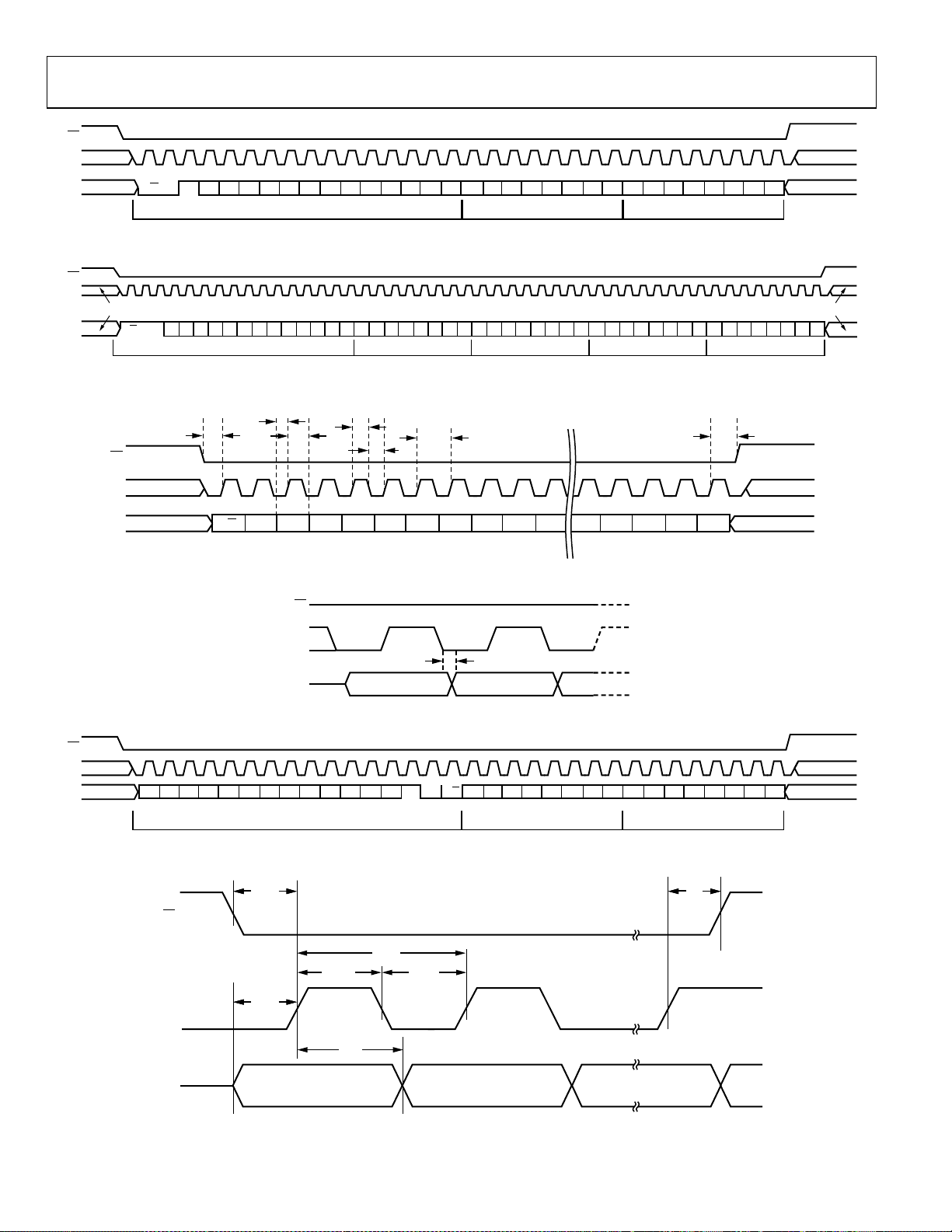
AD9551
CS
DON'T CARE
SCLK
DON'T CARE
SDIO
CS
SCLK
SDIO
DON'T CARE
A12W0W1R/W A11 A10 A9 A8 A7 A6 A5 A4 A3 A2 A1 A0 D7 D6 D5 D4 D3 D2 D1 D0 D7 D6 D5 D4 D3 D2 D1 D0
16-BIT INSTRUCTION HEADER REGISTER (N) DATA REG ISTER (N – 1) DATA
Figure 26. Serial Control Port Write—MSB First, 16-Bit Instruction, Two Bytes Data
DON'T CARE DON'T CARE
A12W0W1R/ W A11A10 A9 A8 A7 A6 A5 A4 A3 A2 A1 A0
D7 D6 D5 D4 D3 D2 D1 D0 D7 D6 D5 D4 D3 D2 D1 D0 D7 D6 D5 D4 D3 D2 D1 D0 D7 D6 D5 D4 D3 D2 D1 D0
REGISTER (N) DATA16-BIT INSTRUCTION HEADER REGISTER (N – 1) DATA REGISTER (N – 2) DATA REGISTER (N – 3) DATA
Figure 27. Serial Control Port Read—MSB First, 16-Bit Instruction, Four Bytes Data
t
CS
SCLK
SDIO
DON'T CARE
DON'T CARE
t
DS
t
S
R/W
t
DH
W1W0A12A11A10A9A8A7A6A5D4D3D2D1D0
t
LOW
HIGH
t
CLK
t
H
DON'T CARE
DON'T CARE
Figure 28. Serial Control Port Write—MSB First, 16-Bit Instruction, Timing Measurements
CS
DON'T CARE
07805-018
7805-016
07805-017
CS
SCLK
SDIO
DON'T CARE
DON'T CARE
SCLK
SDIO
Figure 29. Timing Diagram for Serial Control Port Register Read
A0
A1 A2 A3 A4 A5 A6 A7 A8 A9 A10 A11 A12
16-BIT INSTRUCTION HEADER REGISTER (N) DATA REGI STER (N + 1) DATA
Figure 30. Serial Control Port Write—LSB First, 16-Bit Instruction, Two Bytes Data
t
S
CS
t
HIGH
t
SCLK
SDIO
DS
t
DH
BIT N BIT N + 1
t
DV
DATA BIT N – 1DATA BIT N
D1D0R/WW1W0 D2 D3 D4 D5 D6 D7 D0 D1 D2 D3 D4 D5 D6 D7
t
CLK
t
LOW
Figure 31. Serial Control Port Timing—Write
9
07805-01
DON'T CARE
DON'T CARE
07805-020
t
H
07805-021
Rev. B | Page 28 of 40

AD9551
REGISTER MAP
A bit that is labeled “aclr” is an active high, autoclearing bit. When set to a Logic 1 state, the control logic automatically returns it to
a Logic 0 state upon completion of the indicated task.
Table 22. Register Map
Addr.
(Hex)
0x00 Serial port
0x04 Readback
0x05 I/O update Unused Unused Unused Unused Unused Unused Unused I/O update
0x0A Output PLL
0x0B Output PLL
0x0C Output PLL
0x0D Output PLL
0x0E VCO
0x0F VCO
0x10 VCO
0x11 Output PLL
0x12 Output PLL
0x13 Output PLL
0x14 Output PLL
0x15 Output PLL
0x16 Output PLL
0x17 Output PLL
0x18 Output PLL
Register
Name
control
control
PFD and
charge
pump
PFD and
charge
pump
PFD and
charge
pump
PFD and
charge
pump
control
control
control
control
control
control
control
control
control
control
control
(MSB)
Bit 7
0 LSB first Soft reset
Unused Unused Unused Unused Unused Unused Unused Readback
Enable SPI
control of
charge
pump
current
Unused CP offset
Calibrate
VCO (aclr)
Bit 6 Bit 5 Bit 4 Bit 3 Bit 2 Bit 1
(aclr)
Output PLL PDF and charge pump current control[7:0]
Enable SPI
control of
antibacklash
period
current
polarity
Antibacklash
control[1:0]
Enable
automatic
level
control
MOD[3:0] (output SDM modulus) Enable SPI
FRAC[3:0] (output SDM fractional part) Enable
CP offset current[1:0] Enable CP
Unused Unused Unused Unused Unused Output PLL
Automatic level control threshold[2:0] Enable SPI
VCO level control[5:0] Unused Unused
P1 divider[4:0] P0 divider[2:0]
1 1 Device reset LSB first 0
(3.5 µA granularity, ~900 µA full scale)
CP mode[1:0] Enable CP
mode
control
offset
current
control
VCO band control[6:0] Unused
N[7:0] (output SDM integer part)
MOD[19:12] (output SDM modulus)
MOD[11:4] (output SDM modulus)
control of
output
frequency
FRAC[19:12] (output SDM fractional part)
FRAC[11:4] (output SDM fractional part)
OUTPUT
PLL LOCKED
pin as test
port
PFD
feedback
input edge
control
Reserved/
enable PFD
up divide-
by-2
control of
VCO
calibration
Bypass
output SDM
PFD
reference
input edge
control
Reserved/
enable PFD
down divide-
by-2
Boost VCO
supply
Disable
output SDM
Test mux control[1:0] P
(LSB)
Bit 0
control
(aclr)
Force VCO
to midpoint
frequency
Reserved/
enable
feedback
divide-by-2
lock
detector
powerdown
Enable SPI
control of
VCO band
setting
Reset
output PLL
divider[5]
1
Default
0x18
0x00
0x00
0x80
0x30
0x00
0x00
0x70
0x80
0x80
0x00
0x80
0x00
0x00
0x20
0x00
0x01
0x00
Rev. B | Page 29 of 40

AD9551
Addr.
(Hex)
0x19 Output PLL
0x1A Input
0x1B DCXO
0x1C DCXO
0x1D DCXO
0x1E REFA
0x1F REFA
0x20 REFA
0x21 REFA
0x22 REFA
0x23 REFA
0x24 REFA
0x25 REFA
0x26 REFB
0x27 REFB
0x28 REFB
0x29 REFB
0x2A REFB
0x2B REFB
0x2C REFB
0x2D REFB
Register
Name
control
receiver and
band gap
control
control
control
frequency
frequency
frequency
frequency
frequency
frequency
frequency
frequency
frequency
frequency
frequency
frequency
frequency
frequency
frequency
frequency
(MSB)
Bit 7 Bit 6 Bit 5 Bit 4 Bit 3 Bit 2 Bit 1
Enable SPI
control
of OUT1
dividers
Receiver
reset
(aclr)
Disable
SPI
control of
DCXO
tuning
capacitor
DCXO varactor control[4:0] Select 2×
Enable
SPI
control of
REFA SDM
Must be 0 MODA[18:12] (REFA SDM modulus) 0x80
Enable
SPI
control of
REFB
SDM
Must be 0 MODB[18:12] (REFB SDM modulus) 0x80
Enable SPI
control
of OUT2
divider
Band gap voltage adjust[4:0]
(00000 = maximum, 11111 = minimum)
Enable SPI
control of
DCXO
varactor
DCXO varactor control[12:5] 0x00
Bypass
REFA SDM
FRACA[3:0] (REFA SDM fractional part) Unused Unused Unused Unused 0x00
MODA[3:0] (REFA SDM modulus) Unused Unused Unused Unused 0x00
Bypass
REFB SDM
FRACB[3:0] (REFB SDM fractional part) Unused Unused Unused Unused 0x00
MODB[3:0] (REFB SDM modulus) Unused Unused Unused Unused 0x00
Enable
REFA SDM
NA[5:0] (REFA SDM integer part) Unused Unused 0x40
Enable
REFB
SDM
NB[5:0] (REFB SDM integer part) Unused Unused 0x40
Enable
REFB
FRACA[19:12] (REFA SDM fractional part) 0x40
FRACA[11:4] (REFA SDM fractional part) 0x00
MODA[11:4] (REFA SDM modulus) 0x00
Enable
REFA
FRACB[19:12] (REFB SDM fractional part) 0x40
FRACB[11:4] (REFB SDM fractional part) 0x00
MODB[11:4] (REFB SDM modulus) 0x00
DCXO tuning capacitor control[5:0] 0x80
Unused Disable
Unused Unused Unused Unused 0x30
divider[5:0] 0x20
P
2
Enable
receiver
power-down
frequency
multiplier
REF SDM
PRBS
DCXO bypass Unused 0x00
Select 19.44 MHz input
mode divider
(LSB)
Bit 0
Enable SPI
control of
band gap
voltage
Default
0x00
0x30
Rev. B | Page 30 of 40

AD9551
Addr.
(Hex)
0x2E REFA delay Enable SPI
0x2F REFA delay REFA delay control[1:0] Unused Unused Unused Unused Unused Unused 0x00
0x30 REFB delay Enable SPI
0x31 REFB delay REFB delay control[1:0] Unused Unused Unused Unused Unused Unused 0x00
0x32 OUT1 driver
0x33 Input PLL
0x34 OUT2 driver
Register
Name
control
control
control
(MSB)
Bit 7 Bit 6 Bit 5 Bit 4 Bit 3 Bit 2 Bit 1
control of
REFA
delay
control of
REFB
delay
OUT1
drive
strength
Loop filter
sample
rate
control
OUT2
drive
strength
OUT1
powerdown
Select 2×
frequency
divider
OUT2
powerdown
OUT1 mode control[2:0] OUT1 CMOS polarity[1:0] Enable SPI
Select crystal
frequency[1:0]
OUT2 mode control[2:0] OUT2 CMOS polarity[1:0] Enable SPI
REFA delay control[8:2] 0x40
REFB delay control[8:2] 0x40
Unused Unused Unused Unused 0x00
(LSB)
Bit 0
control of
OUT1 driver
control
control of
OUT2 driver
control
Default
0xA8
0xA8
Rev. B | Page 31 of 40

AD9551
REGISTER MAP DESCRIPTIONS
Control bit functions are active high, and register address values are always hexadecimal, unless otherwise noted.
Serial Port Control (Register 0x00 to Register 0x05)
Table 23.
Address Bit Bit Name Description
0x00 7 Unused Forced to Logic 0 internally, which enables 3-wire mode only.
6 LSB first Bit order for SPI port.
0 = most significant bit and byte first (default).
1 = least significant bit and byte first.
5 Soft reset Software initiated reset (register values set to default). This is an autoclearing bit.
4 Unused
[3:0] Unused Mirrored version of the contents of Register 0x00[7:4] (that is, Bits[3:0] = Bits[7:4]).
0x04 [7:1] Unused Unused.
0 Readback control
0 = reads values currently applied to the internal logic of the device (default).
1 = reads buffered values that take effect on next assertion of I/O update.
0x05 [7:1] Unused Unused.
0 I/O update
Forced to Logic 1 internally, which enables 16-bit mode (the only mode supported by
the device).
For buffered registers, serial port readback reads from actual (active) registers instead of
from the buffer.
Writing a 1 to this bit transfers the data in the serial I/O buffer registers to the internal
control registers of the device. This is an autoclearing bit.
Output PLL PFD and Charge Pump Control (Register 0x0A to Register 0x0D)
Table 24.
Address Bit Bit Name Description
0x0A [7:0]
0x0B 7
0 = normal VCO operation (default).
1 = force VCO control voltage to midscale.
Output PLL PFD and charge
pump current control
Enable SPI control of charge
pump current
1 = charge pump current defined by Register 0x0A.
6
Enable SPI control of
antibacklash period
1 = antibacklash period defined by Register 0x0D[7:6].
[5:4] CP mode Controls the mode of the output PLL charge pump.
00 = tristate.
01 = pump up.
10 = pump down.
11 = normal (default).
3 Enable CP mode control Controls functionality Bits[5:4] (CP mode).
0 = the device automatically controls the charge pump mode (default).
1 = charge pump mode is defined by Bits[5:4].
2 PFD feedback input edge control Selects the polarity of the active edge of the output PLL’s feedback input.
1 = negative edge.
1 PFD reference input edge control Selects the polarity of the active edge of the output PLL’s reference input.
0 = positive edge (default).
1 = negative edge.
0 Force VCO to midpoint frequency Selects VCO control voltage functionality.
These bits set the magnitude of the output PLL charge pump current. The granularity
is ~3.5 A with a full-scale magnitude of ~900 A. Register 0x0A is ineffective unless
Register 0x0B[7] = 1. Default is 0x80, or ~448 A.
Controls functionality of Register 0x0A.
0 = the device automatically controls the charge pump current (default).
Controls functionality of Register 0x0D[7:6].
0 = the device automatically controls the antibacklash period (default).
0 = positive edge (default).
Rev. B | Page 32 of 40

AD9551
Address Bit Bit Name Description
0x0C 7 Unused Unused.
6 CP offset current polarity Selects the polarity of the charge pump offset current of the output PLL.
0 = pump up (default).
1 = pump down.
This bit is ineffective unless Bit 3 = 1.
[5:4] CP offset current
00 = 1/2 (default).
01 = 1/4.
10 = 1/8.
11 = 1/16.
3 Enable CP offset current control Controls functionality of Bits[6:4].
0 = the device automatically controls charge pump offset current (default).
1 = charge pump offset current defined by Bits[6:4].
2 Reserved Enables PFD up divide-by-2 (reserved for test).
1 Reserved Enables PFD down divide-by-2 (reserved for test).
0 Reserved Enables feedback divide-by-2 (reserved for test).
0x0D [7:6] Antibacklash control Controls the PFD antibacklash period of the output PLL.
00 = minimum (default).
01 = low.
10 = high.
11 = maximum.
These bits are ineffective unless Register 0x0B[6] = 1.
[5:1] Unused Unused.
0
Output PLL lock detector
power-down
1 = lock detector powered down.
Controls the magnitude of the charge pump offset current of the output PLL as a
fraction of the value in Register 0x0A. Ineffective unless Bit 3 = 1.
Controls power-down of the output PLL’s lock detector.
0 = lock detector active (default).
VCO Control (Register 0x0E to Register 0x10)
Table 25.
Address Bit Bit Name Description
0x0E 7 Calibrate VCO Initiates VCO calibration (this is an autoclearing bit). This bit is ineffective unless Bit 2 = 1.
6 Enable automatic level control Enables automatic level control of the VCO.
0 = VCO level defined by Register 0x0F[7:2].
1 = the device automatically controls the VCO level (default).
[5:3]
Automatic level control
threshold
2
Enable SPI control of VCO
calibration
1 Boost VCO supply Selects VCO supply voltage.
0
Enable SPI control of VCO band
setting
0x0F [7:2] VCO level control
[1:0] Unused Unused.
0x10 [7:1] VCO band control
0 Unused Unused.
Controls the VCO threshold detector level. The default is 110. Note that the functionality of Bit 4 is inverted; that is, the minimum is 010, and the maximum is 101.
Enables functionality of Bit 7.
0 = the device automatically performs VCO calibration (default).
1 = Bit 7 controls VCO calibration.
0 = normal supply voltage (default).
1 = increase supply voltage by 100 mV.
Controls VCO band setting functionality.
0 = the device automatically selects the VCO band (default).
1 = VCO band defined by Register 0x10[7:1].
Controls the VCO amplitude from minimum (00 0000) to maximum (11 1111). The
default is 10 0000. These bits are ineffective unless Register 0x0E[6] = 0.
Controls the VCO frequency band from minimum (000 0000) to maximum (111 1111).
The default is 100 0000.
Rev. B | Page 33 of 40

AD9551
Output PLL Control (Register 0x11 to Register 0x19)
Table 26.
Address Bit Bit Name Description
0x11 [7:0] N
0x12 [7:0] MOD Bits[19:12] of the 20-bit modulus of the output SDM.
0x13 [7:0] MOD Bits[11:4] of the 20-bit modulus of the output SDM.
0x14 [7:4] MOD
3
Enable SPI control of
output frequency
2 Bypass output SDM Controls bypassing of the output SDM.
1 Disable output SDM Controls the output SDM internal clocks.
0 Reset output PLL Controls initialization of the output PLL.
0x15 [7:0] FRAC Bits[19:12] of the 20-bit fractional part of the output SDM.
0x16 [7:0] FRAC Bits[11:4] of the 20-bit fractional part of the output SDM.
0x17 [7:4] FRAC Bits[3:0] of the 20-bit fractional part of the output SDM.
3
Enable OUTPUT PLL
LOCKED pin as test port
[2:1] Test mux control Selects test mux output.
0 P1 divider Bit 5 of the 6-bit P1 divider for OUT1.
0x18 [7:3] P1 divider
[2:0] P0 divider Bits[2:0] of the 3-bit P0 divider for OUT1. The P0 divide value is as follows:
0x19 7
Enable SPI control of
OUT1 dividers
6
Enable SPI control of
OUT2 divider
[5:0] P2 divider
8-bit integer divide value for the output SDM. Default is 0x00.
Note that operational limitations impose a lower boundary of 64 (0x40) on N.
Bits[3:0] of the 20-bit modulus of the output SDM.
Default is MOD = 1000 0000 0000 0000 0000 (524,288).
Controls output frequency functionality.
0 = output frequency defined by the Y[3:0] pins (default).
1 = contents of Register 0x11 to Register 0x17 define output frequency via N, MOD, and FRAC.
0 = allow integer-plus-fractional division (default).
1 = allow only integer division.
0 = normal operation (SDM clocks active) (default).
1 = SDM disabled (SDM clocks stopped).
0 = normal operation (default).
1 = resets the counters and logic associated with the output PLL but does not affect the
output dividers.
Default is FRAC = 0010 0000 0000 0000 0000 (131,072).
Controls functionality of the OUTPUT PLL LOCKED pin (Pin 26).
0 = OUTPUT PLL LOCKED pin indicates status of PLL lock detector (default).
1 = OUTPUT PLL LOCKED pin indicates the signal defined by Bits[2:1].
00 = front end test clock (default).
01 = PFD up divide-by-2.
10 = PFD down divide-by-2.
11 = PLL feedback divide-by-2.
These bits are ineffective unless Bit 3 = 1.
Bits[4:0] of the 6-bit P
P
= 100000 (32). The P1 bits are ineffective unless Register 0x19[7] = 1.
1
divider for OUT1 (1 ≤ P1 ≤ 63). Do not set these bits to 000000. Default is
1
000 = 4 (default).
001 = 5.
010 = 6.
011 = 7.
100 = 8.
101 = 9.
110 = 10.
111 = 11.
bits are ineffective unless Register 0x19[7] = 1.
The P
0
Controls functionality of OUT1 dividers.
0 = OUT1 dividers defined by the Y[3:0] pins (default).
1 = contents of Register 0x17 and Register 0x18 define OUT1 dividers (P
and P1).
0
Controls functionality of OUT2 divider.
0 = OUT2 divider defined by the Y[3:0] pins (P
1 = contents of Bits[5:0] define P
Bits[5:0] of the 6-bit P
P
= 100000 (32). The P2 bits are ineffective unless Register 0x19[6] = 1.
2
divider for OUT2 (1 ≤ P2 ≤ 63). Do not set these bits to 000000. Default is
2
.
2
= 1) (default).
2
Rev. B | Page 34 of 40

AD9551
Input Receiver and Band Gap (Register 0x1A)
Table 27.
Address Bit Bit Name Description
0x1A 7 Receiver reset Input receiver reset control. This is an autoclearing bit.
0 = normal operation (default).
1 = reset input receiver logic.
[6:2] Band gap voltage adjust
1 Enable receiver power-down
0 = option disabled (default).
1 = option enabled.
0
Enable SPI control of band gap
voltage
1 = Bits[6:2] define the receiver band gap voltage.
DCXO Control (Register 0x1B to Register 0x1D)
Table 28.
Address Bit Bit Name Description
0x1B 7
0x1C [7:0] DCXO varactor control Bits[12:5] of the 13-bit varactor control word.
0x1D [7:3] DCXO varactor control
Disable SPI control of DCXO
tuning capacitor
1 = the device automatically selects DCXO tuning capacitance (default).
6
Enable SPI control of DCXO
varactor
1 = varactor defined by Register 0x1C[7:0] and Register 0x1D[7:3].
[5:0] DCXO tuning capacitor control
2 Select 2× frequency multiplier Select/bypass the 2× frequency multiplier.
0 = bypassed (default).
1 = selected.
1 DCXO bypass Select/bypass the DCXO.
0 = selected (default).
1 = bypassed.
0 Unused Unused.
Controls the band gap voltage setting from minimum (0 0000) to maximum (1 1111).
Default is 0 0000.
Controls the option to power down the REFA and/or REFB receiver via Register 0x26[4]
and Register 0x1E[4], respectively.
Enables functionality of Bits[6:2].
0 = the device automatically selects receiver band gap voltage (default).
Disables functionality of Bits[5:0].
0 = tuning capacitance defined by Bits[5:0].
Enables functionality of Register 0x1C and Register 0x1D[7:3].
0 = the device automatically selects DCXO varactor (default).
Higher binary values correspond to smaller total capacitance, resulting in a higher
operating frequency. Default is 00 0000.
Bits[4:0] of the 13-bit varactor control word. The default varactor control word is
0 0000 0000 0000.
Rev. B | Page 35 of 40

AD9551
REFA Frequency Control (Register 0x1E to Register 0x25)
Table 29.
Address Bit Bit Name Description
0x1E 7
0x1F [7:0] FRACA Bits[19:12] of the 20-bit fractional part of the REFA SDM.
0x20 [7:0] FRACA Bits[11:4] of the 20-bit fractional part of the REFA SDM.
0x21 [7:4] FRACA Bits[3:0] of the 20-bit fractional part of the REFA SDM.
0x22 [7:2] NA 6-bit integer divide value for the REFA SDM. Default divide value is 16.
0x23 7 Unused This bit must be programmed to 0, even though the default value is 1.
0x24 [7:0] MODA Bits[11:4] of the 19-bit modulus of the REFA SDM.
0x25 [7:4] MODA Bits[3:0] of the 19-bit modulus of the REFA SDM.
Enable SPI control of
REFA SDM
6 Bypass REFA SDM Controls bypassing of the REFA SDM.
5 Enable REFA SDM Controls REFA SDM enable and hold functionality.
4 Enable REFB Controls REFB enable and power-down functionality.
3 Unused Unused.
2 Disable REF SDM PRBS Controls the PRBS generator for both the REFA and REFB SDMs.
[1:0]
Select 19.44 MHz input
mode divider
[3:0] Unused Unused.
[1:0] Unused Unused.
[6:0] MODA Bits[18:12] of the 19-bit modulus of the REFA SDM.
[3:0] Unused Unused.
Controls REFA frequency division functionality.
0 = REFA frequency division, as defined by the A[3:0] pins (default).
1 = contents of Register 0x1F to Register 0x25 define REFA frequency division via NA,
MODA, and FRACA.
0 = allow integer-plus-fractional division (default).
1 = allow only integer division.
0 = reset REFA SDM and stop its clocks.
1 = REFA SDM enabled (default).
0 = power down REFB input receiver (ineffective unless Register 0x1A[1] = 1).
1 = normal operation (default).
0 = PRBS generator enabled (default).
1 = PRBS generator disabled.
Selects the divider value when the 19.44 MHz input mode is in effect.
00 = 1 (default).
01 = 1.
10 = 2.
11 = 4.
These bits are ineffective unless the A[3:0] pins = 1111 or the B[3:0] pins = 1111.
Default is FRACA = 0100 0000 0000 0000 0000 (262,144).
Note that FRACA assumes twos complement format.
Default is MODA = 000 0000 0000 0000 0000.
Rev. B | Page 36 of 40

AD9551
REFB Frequency Control (Register 0x26 to Register 0x2D)
Table 30.
Address Bit Bit Name Description
0x26 7
0x27 [7:0] FRACB Bits[19:12] of the 20-bit fractional part of the REFB SDM.
0x28 [7:0] FRACB Bits[11:4] of the 20-bit fractional part of the REFB SDM.
0x29 [7:4] FRACB Bits[3:0] of the 20-bit fractional part of the REFB SDM.
0x2A [7:2] NB 6-bit integer divide value for the REFB SDM. Default divide value is 8.
0x2B 7 Unused This bit must be programmed to 0, even though the default value is 1.
0x2C [7:0] MODB Bits[11:4] of the 19-bit modulus of the REFB SDM.
0x2D [7:4] MODB Bits[3:0] of the 19-bit modulus of the REFB SDM.
Enable SPI control of
REFB SDM
6 Bypass REFB SDM Controls bypassing of the REFB SDM.
5 Enable REFB SDM Controls REFB SDM enable and hold functionality.
4 Enable REFA Controls REFA enable and power-down functionality.
[3:0] Unused Unused.
[3:0] Unused Unused.
[1:0] Unused Unused.
[6:0] MODB Bits[18:12] of the 19-bit modulus of the REFB SDM.
[3:0] Unused Unused.
Controls REFB frequency division functionality.
0 = REFB frequency division defined by the B[3:0] pins (default).
1 = contents of Register 0x27 to Register 0x2D define REFB frequency division via NB,
MODB, and FRACB.
0 = allow integer-plus-fractional division (default).
1 = allow integer division only.
0 = reset REFB SDM and stop its clocks.
1 = REFB SDM enabled (default).
0 = power down REFA input receiver (ineffective unless Register 0x1A[1] = 1).
1 = normal operation (default).
Default is FRACB = 0100 0000 0000 0000 0000 (262,144).
Note that FRACB assumes twos complement format.
Default is MODB = 000 0000 0000 0000 0000.
REFA Delay Control (Register 0x2E and Register 0x2F)
Table 31.
Address Bit Bit Name Description
0x2E 7
0x2F [7:6] REFA delay control Bits[1:0] of the 9-bit REFA delay word.
Enable SPI control of REFA
delay
[6:0] REFA delay control Bits[8:2] of the 9-bit REFA delay word.
[5:0] Unused Unused.
Controls REFA delay functionality.
0 = the device automatically selects REFA delay (default).
1 = REFA delay defined by Register 0x2E[6:0] and Register 0x2F[7:6].
Default is 1 0000 0000. Delay granularity is ~150 ps.
REFB Delay Control (Register 0x30 and Register 0x31)
Table 32.
Address Bit Bit Name Description
0x30 7
0x31 [7:6] REFB delay control Bits[1:0] of the 9-bit REFB delay word.
Enable SPI control of REFB
delay
[6:0] REFB delay control Bits[8:2] of the 9-bit REFB delay word.
[5:0] Unused Unused.
Controls REFB delay functionality:
0 = the device automatically selects REFB delay (default).
1 = REFB delay defined by Register 0x30[6:0] and Register 0x31[7:6].
Default is 1 0000 0000. Delay granularity is ~150 ps.
Rev. B | Page 37 of 40

AD9551
OUT1 Driver Control (Register 0x32)
Table 33.
Address Bit Bit Name Description
0x32 7 OUT1 drive strength Controls the output drive capability of the OUT1 driver.
0 = weak.
1 = strong (default).
6 OUT1 power-down Controls power-down functionality of the OUT1 driver.
0 = OUT1 active (default).
1 = OUT1 powered down.
[5:3] OUT1 mode control OUT1 driver mode selection.
000 = CMOS, both pins active.
001 = CMOS, positive pin active, negative pin tristate.
010 = CMOS, positive pin tristate, negative pin active.
011 = CMOS, both pins tristate.
100 = LVDS.
101 = LVPECL (default).
110 = not used.
111 = not used.
[2:1] OUT1 CMOS polarity Selects the polarity of the OUT1 pins in CMOS mode.
00 = positive pin logic is true = 1, false = 0/negative pin logic is true = 0, false = 1 (default).
01 = positive pin logic is true = 1, false = 0/negative pin logic is true = 1, false = 0.
10 = positive pin logic is true = 0, false = 1/negative pin logic is true = 0, false = 1.
11 = positive pin logic is true = 0, false = 1/negative pin logic is true = 1, false = 0.
These bits are ineffective unless Bits[5:3] select CMOS mode.
0
Enable SPI control of OUT1
driver control
1 = OUT1 functionality defined by Bits[7:1].
Controls OUT1 driver functionality.
0 = OUT1 is LVDS or LVPECL, per the OUTSEL pin (Pin 16) (default).
Input PLL Control (Register 0x33)
Table 34.
Address Bit Bit Name Description
0x33 7 Loop filter sample rate control Select/bypass 8× clock divider to the digital loop filter.
0 = selected (default).
1 = bypassed.
6 Select 2× frequency divider Select/bypass the 2× frequency divider.
0 = bypassed (default).
1 = selected.
Note that this bit is not functional in 19.44 MHz mode.
[5:4] Select crystal frequency Select the crystal frequency for 19.44 MHz mode.
00 = 52.000 MHz (default).
01 = 50.000 MHz.
10 = 49.860 MHz.
11 = 49.152 MHz.
Note that these bits are functional only in 19.44 MHz mode.
[3:0] Unused Unused.
Rev. B | Page 38 of 40

AD9551
OUT2 Driver Control (Register 0x34)
Table 35.
Address Bit Bit Name Description
0x34 7 OUT2 drive strength Controls the output drive capability of the OUT2 driver.
0 = weak.
1 = strong (default).
6 OUT2 power-down Controls power-down functionality of the OUT2 driver.
0 = OUT2 active (default).
1 = OUT2 powered down.
[5:3] OUT2 mode control OUT2 driver mode selection.
000 = CMOS, both pins active.
001 = CMOS, positive pin active, negative pin tristate.
010 = CMOS, positive pin tristate, negative pin active.
011 = CMOS, both pins tristate.
100 = LVDS.
101 = LVPECL (default).
110 = not used.
111 = not used.
[2:1] OUT2 CMOS polarity Selects the polarity of the OUT2 pins in CMOS mode.
00 = positive pin logic is true = 1, false = 0/negative pin logic is true = 0, false = 1 (default).
01 = positive pin logic is true = 1, false = 0/negative pin logic is true = 1, false = 0.
10 = positive pin logic is true = 0, false = 1/negative pin logic is true = 0, false = 1.
11 = positive pin logic is true = 0, false = 1/negative pin logic is true = 1, false=0.
These bits are ineffective unless Bits[5:3] select CMOS mode.
0
Enable SPI control of OUT2
driver control
1 = OUT2 functionality defined by Bits[7:1].
Controls OUT2 driver functionality.
0 = OUT2 is LVDS or LVPECL, per the OUTSEL pin (Pin 16) (default).
Rev. B | Page 39 of 40

AD9551
S
OUTLINE DIMENSIONS
6.00
INDICATOR
1.00
0.85
0.80
EATING
PLANE
PIN 1
12° MAX
BSC SQ
5.75
BSC SQ
TOP VIEW
0.80 MAX
0.65 TYP
0.30
0.23
0.18
COMPLIANT TO JEDEC STANDARDS MO-220-VJJD-2
0.20 REF
0.05 MAX
0.02 NOM
COPLANARIT Y
0.60 MAX
0.50
BSC
0.50
0.40
0.30
0.08
Figure 32. 40-Lead Lead Frame Chip Scale Package [LFCSP_VQ]
6 × 6 mm Body, Very Thin Quad
(CP-40-8)
Dimensions shown in millimeters
ORDERING GUIDE
Model Temperature Range Package Description Package Option
AD9551BCPZ
AD9551BCPZ-REEL7
AD9551/PCBZ
1
Z = RoHS Compliant Part.
1
–40°C to +85°C 40-Lead Lead Frame Chip Scale Package [LFCSP_VQ] CP-40-8
1
–40°C to +85°C 40-Lead Lead Frame Chip Scale Package [LFCSP_VQ] CP-40-8
1
Evaluation Board
0.60 MAX
29
28
20
19
BOTTOM VIEW
40
1
EXPOSED
PAD
10
11
4.50
REF
FOR PROPER CONNECTION O F
THE EXPOSED PAD, REFER TO
THE PIN CONF IGURATIO N AND
FUNCTION DES CRIPTIONS
SECTION O F THIS DAT A SHEET.
PIN 1
INDICATOR
3.05
2.90 SQ
2.75
0.25 MIN
082708-A
©2009 Analog Devices, Inc. All rights reserved. Trademarks and
registered trademarks are the property of their respective owners.
D07805-0-9/09(B)
Rev. B | Page 40 of 40
 Loading...