Quad/Octal Input Network Clock
FEATURES
Supports Stratum 2 stability in holdover mode
Supports reference switchover with phase build-out
Supports hitless reference switchover
Auto/manual holdover and reference switchover
4 pairs of reference input pins with each pair configurable as
a single differential input or as 2 independent single-
ended inputs
Input reference frequencies from 1 Hz to 750 MHz
Reference validation and frequency monitoring (1 ppm)
Programmable input reference switchover priority
30-bit programmable input reference divider
4 pairs of clock output pins with each pair configurable as a
single differential LVDS/LVPECL output or as 2 single-
ended CMOS outputs
Output frequencies up to 450 MHz
30-bit integer and 10-bit fractional programmable feedback
divider
Programmable digital loop filter covering loop bandwidths
from 0.001 Hz to 100 kHz
Optional low noise LC-VCO system clock multiplier
Optional crystal resonator for system clock input
On-chip EEPROM to store multiple power-up profiles
Software controlled power-down
88-lead LFCSP package
Generator/Synchronizer
AD9548
APPLICATIONS
Network synchronization
Cleanup of reference clock jitter
GPS 1 pulse per second synchronization
SONET/SDH clocks up to OC-192, including FEC
Stratum 2 holdover, jitter cleanup, and phase transient
control
Stratum 3E and Stratum 3 reference clocks
Wireless base station controllers
Cable infrastructure
Data communications
GENERAL DESCRIPTION
The AD9548 provides synchronization for many systems,
including synchronous optical networks (SONET/SDH). The
AD9548 generates an output clock synchronized to one of up to
four differential or eight single-ended external input references.
The digital PLL allows for reduction of input time jitter or phase
noise associated with the external references. The AD9548
continuously generates a clean (low jitter), valid output clock
even when all references have failed by means of a digitally
controlled loop and holdover circuitry.
The AD9548 operates over an industrial temperature range of
−40°C to +85°C.
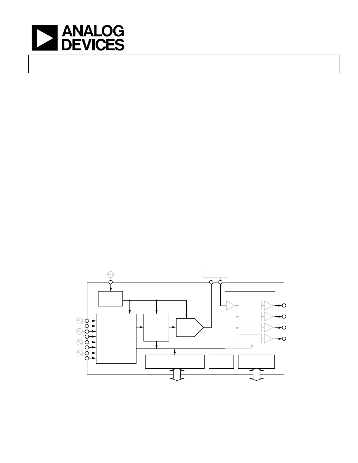
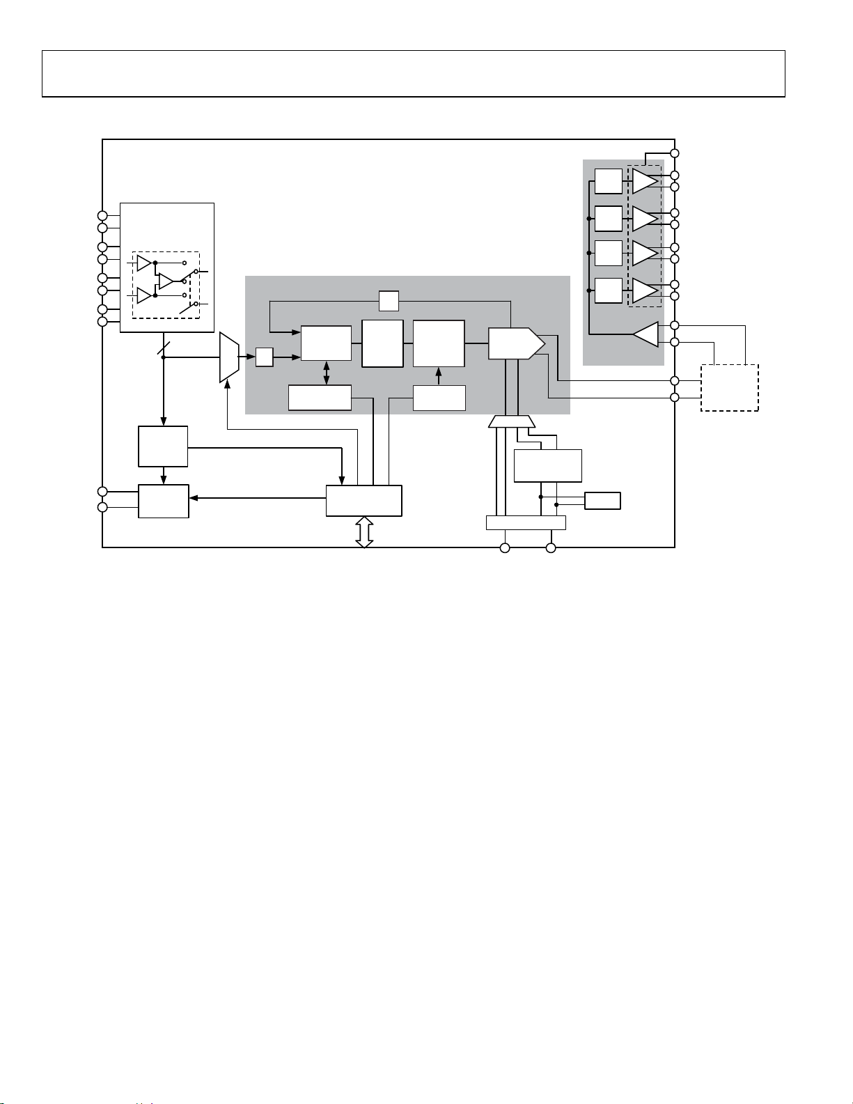
FUNCTIONAL BLOCK DIAGRAM
STABLE
SOURCE
CLOCK
MULTIPLIER
DIGITAL
REFERENCE INPU TS
AND
MONITOR MUX
Rev. B
Information furnished by Analog Devices is believed to be accurate and reliable. However, no
responsibility is assumed by Anal og Devices for its use, nor for any infringements of patents or ot her
rights of third parties that may result from its use. Specifications subject to change without notice. No
license is granted by implication or otherwise under any patent or patent rights of Analog Devices.
Trademarks and registered trademarks are the property of their respective owners.
PLL
SERIAL CONT ROL INT ERFACE
(SPI or I
AD9548
DAC
2
C)
Figure 1.
ANALOG
FILTER
CLOCK DISTRI BUTION
CHANNEL 0
DIVIDER
CHANNEL 1
DIVIDER
CHANNEL 2
DIVIDER
CHANNEL 3
DIVIDER
SYNC
EEPROM
One Technology Way, P.O. Box 9106, Norwood, MA 02062-9106, U.S.A.
Tel: 781.329.4700 www.analog.com
Fax: 781.461.3113 ©2009–2011 Analog Devices, Inc. All rights reserved.
STATUS AND
CONTROL PINS
08022-001

AD9548
TABLE OF CONTENTS
Features.............................................................................................. 1
Applications....................................................................................... 1
General Description ......................................................................... 1
Functional Block Diagram .............................................................. 1
Revision History ............................................................................... 3
Specifications..................................................................................... 4
Supply Voltage............................................................................... 4
Supply Current.............................................................................. 4
Power Dissipation......................................................................... 4
Logic Inputs (M7 to M0, RESET, TDI, TCLK, TMS).............. 5
Logic Outputs (M7 to M0, IRQ, TDO) ..................................... 5
System Clock Inputs (SYSCLKP/SYSCLKN) ........................... 5
Distribution Clock Inputs (CLKINP/CLKINN)...................... 6
Reference Inputs (REFA/REFAA to REFD/REFDD) .............. 7
Reference Monitors...................................................................... 7
Reference Switchover Specifications.......................................... 8
Distribution Clock Outputs (OUT0 to OUT3)........................ 8
DAC Output Characteristics (DACOUTP/DACOUTN) .......9
Time Duration of Digital Functions........................................ 10
Digital PLL .................................................................................. 10
Digital PLL Lock Detection ...................................................... 10
Holdover Specifications............................................................. 10
Serial Port Specifications—SPI Mode...................................... 11
Serial Port Specifications—I2C Mode...................................... 11
Jitter Generation .........................................................................12
Absolute Maximum Ratings.......................................................... 14
ESD Caution................................................................................ 14
Pin Configuration and Function Descriptions........................... 15
Typical Performance Characteristics ........................................... 18
Input/Output Termination Recommendations .......................... 23
Getting Started................................................................................ 24
Power-On Reset .......................................................................... 24
Initial Pin Programming ...........................................................24
Device Register Programming.................................................. 24
Theory of Operation ...................................................................... 26
Overview...................................................................................... 26
Reference Clock Inputs.............................................................. 27
Reference Monitors .................................................................... 27
Reference Profiles....................................................................... 28
Reference Switchover ................................................................. 30
Rev. B | Page 2 of 112
Digital PLL (DPLL) Core .......................................................... 32
Direct Digital Synthesizer ......................................................... 34
Tuning Word Processing ........................................................... 35
Loop Control State Machine..................................................... 36
System Clock Inputs................................................................... 37
SYSCLK PLL Multiplier............................................................. 38
Clock Distribution ..................................................................... 39
Status and Control.......................................................................... 44
Multifunction Pins (M0 to M7) ............................................... 44
IRQ Pin........................................................................................ 45
Watchdog Timer......................................................................... 46
EEPROM ..................................................................................... 46
Serial Control Port ......................................................................... 51
SPI/IC Port Selection................................................................ 51
SPI Serial Port Operation.......................................................... 51
IC Serial Port Operation.......................................................... 55
I/O Programming Registers.......................................................... 58
Buffered/Active Registers.......................................................... 58
Autoclear Registers..................................................................... 58
Register Access Restrictions...................................................... 59
Register Map ................................................................................... 60
Register Map Bit Descriptions...................................................... 70
Serial Port Configuration (Register 0000 to Register 0005). 70
System Clock (Register 0100 to Register 0108)...................... 71
General Configuration (Register 0200 to Register 0214) ..... 72
DPLL Configuration (Register 0300 to Register 031B)......... 75
Clock Distribution Output Configuration (Register 0400 to
Register 0419) ............................................................................. 77
Reference Input Configuration (Register 0500 to Register
0507)............................................................................................. 81
Profile Registers (Register 0600 to Register 07FF) ................ 83
Operational Controls (Register 0A00 to Register 0A10)...... 92
Status Readback (Register 0D00 to Register 0D19)............... 97
Nonvolatile Memory (EEPROM) Control (Register 0E00 to
Register 0E03)........................................................................... 100
EEPROM Storage Sequence (Register 0E10 to Register 0E3F)
..................................................................................................... 101
Power Supply Partitions............................................................... 105
3.3 V Supplies............................................................................ 105
1.8 V Supplies............................................................................ 105
Thermal Performance.................................................................. 106

AD9548
Calculating Digital Filter Coefficients....................................... 107
Calculation of the α Register Values ..................................... 108
Calculation of the β Register Values...................................... 108
Calculation of the γ Register Values ...................................... 109
REVISION HISTORY
7/11—Rev. A to Rev. B
Changed AD9584 to AD9548........................................................32
Changed 437,749,988,378,041 to 43,774,988,378,041................34
Change to Calculating Digital Filter Coefficients Section.......107
10/10—Rev. 0 to Rev. A
Changes to Timing Parameter, Table 17.......................................11
Added Low Loop Bandwidth Applications Using a TCXO/OCXO
Section and Choosing a System Clock Oscillator Frequency
Section ..............................................................................................37
Moved System Clock Period Section ............................................39
Changes to Addr 0002, Table 35....................................................60
Changes to Addr 0600, Table 35....................................................62
Changes to Addr 0632, Table 35....................................................63
Calculation of the δ Register Values.......................................109
Outline Dimensions......................................................................110
Ordering Guide.........................................................................110
Changes to Addr 0680, Table 35....................................................64
Changes to Addr 06B2, Table 35...................................................65
Changes to Address 0002 Description, Table 38.........................70
Changes to Bit 7 and Bit 6, Table 78 .............................................83
Changes to Address 0629 and Address 062A, Table 87 and Bit 7
and Bit 6, Table 88...........................................................................85
Changes to Address 065B and Address 065C, Table 97 and Bit 7
and Bit 6, Table 98...........................................................................87
Changes to Address 06A9 and Address 06AA, Table 107 .........89
Changes to Bit 7 and Bit 6, Table 108 ...........................................90
Changes to Address 06DB and Address 06DC, Table 117.........92
4/09—Revision 0: Initial Version
Rev. B | Page 3 of 112

AD9548
SPECIFICATIONS
Minimum (min) and maximum (max) values apply for the full range of supply voltage and operating temperature variations. Typical (typ)
values apply for AVDD3 = DVDD_I/O = 3.3 V; AVDD = DVDD
SUPPLY VOLTAGE
Table 1.
Parameter Min Typ Max Unit Test Conditions/Comments
SUPPLY VOLTAGE
DVDD3 3.135 3.30 3.465 V Pin 7, Pin 82
DVDD 1.71 1.80 1.89 V Pin 1, Pin 6, Pin 12, Pin 14, Pin 15, Pin 77, Pin 83, Pin 88
AVDD3 3.135 3.30 3.465 V Pin 21, Pin 22, Pin 47, Pin 60, Pin 66, Pin 67, Pin 73
3.3 V Supply (Typical) 3.135 3.30 3.465 V Pin 31, Pin 37, Pin 38, Pin 44
1.8 V Supply (Alternative) 1.71 1.80 1.89 V Pin 31, Pin 37, Pin 38, Pin 44
AVDD 1.71 1.80 1.89 V
SUPPLY CURRENT
The test conditions for the maximum (max) supply current are the same as the test conditions for the All Blocks Running parameter of Tab l e 3 .
The test conditions for the typical (typ) supply current are the same as the test conditions for the Typical Configuration parameter of Ta ble 3 .
Table 2.
Parameter Min Typ Max Unit Test Conditions/Comments
SUPPLY CURRENT
I
1.5 3 mA Pin 7, Pin 82
DVDD3
I
190 215 mA Pin 1, Pin 6, Pin 12, Pin 14, Pin 15, Pin 77, Pin 83, Pin 88
DVDD
I
52 75 mA Pin 21, Pin 22, Pin 47, Pin 60, Pin 66, Pin 67, Pin 73
AVDD3
I
AVDD3
3.3 V Supply (Typical) 24 110 mA Pin 31, Pin 37, Pin 38, Pin 44
1.8 V Supply (Alternative) 24 110 mA Pin 31, Pin 37, Pin 38, Pin 44
I
135 163 mA
AVDD
= 1.8 V; TA= 25°C; I
Pin 23, Pin 24, Pin 29, Pin 34, Pin 41, Pin 50, Pin 55, Pin 59,
Pin 63, Pin 70, Pin 74
Pin 23, Pin 24, Pin 29, Pin 34, Pin 41, Pin 50, Pin 55, Pin 59,
Pin 63, Pin 70, Pin 74
= 20 mA (full scale), unless otherwise noted.
DAC
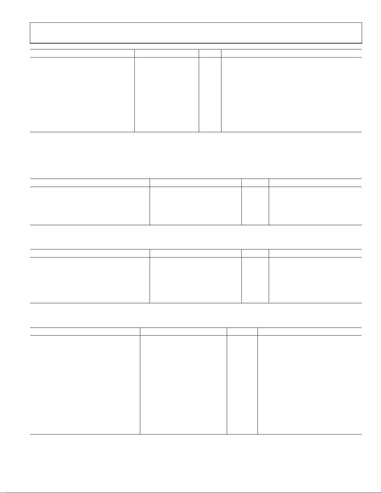
POWER DISSIPATION
Table 3.
Parameter Min Typ Max Unit Test Conditions/Comments
POWER DISSIPATION
Typical Configuration 800 1100 mW
All Blocks Running 900 1400 mW
Full Power-Down 13 mW
Rev. B | Page 4 of 112
= 20 MHz1; fS = 1 GHz2; f
f
SYSCLK
= 122.88 MHz3; one
DDS
LVPECL clock distribution output running at 122.88 MHz
(all others powered down); one input reference running
at 100 MHz (all others powered down)
= 20 MHz1; fS = 1 GHz2; f
f
SYSCLK
= 399 MHz3; all clock
DDS
distribution outputs configured as LVPECL at 399 MHz; all
input references configured as differential at 100 MHz;
fractional-N active (R = 10, S = 39, U = 9, V = 10)
Conditions = typical configuration; no external pull-up or
pull-down resistors
AD9548
Parameter Min Typ Max Unit Test Conditions/Comments
Incremental Power Dissipation
SYSCLK PLL Off −105 mW f
Input Reference On
Differential 7 mW
Single-Ended 13 mW
Output Distribution Driver On
LVDS 70 mW
LVPECL 75 mW
CMOS 65 mW A single 3.3 V CMOS output with a 10 pF load.
1
f
is the frequency at the SYSCLKP and SYSCLKN pins.
SYSCLK
2
fS is the sample rate of the output DAC.
3
f
is the output frequency of the DDS.
DDS
LOGIC INPUTS (M7 TO M0, RESET, TDI, TCLK, TMS)
Table 4.
Parameter Min Typ Max Unit Test Conditions/Comments
LOGIC INPUTS (M7 to M0, RESET, TDI, TCLK, TMS)
Input High Voltage (VIH) 2.1 V
Input Low Voltage (VIL) 0.8 V
Input Current (I
Input Capacitance (CIN) 3 pF
, I
) ±80 ±200 µA
INH
INL
Conditions = typical configuration; table values show the
change in power due to the indicated operation.
= 1 GHz1; high frequency direct input mode.
SYSCLK
LOGIC OUTPUTS (M7 TO M0, IRQ, TDO)
Table 5.
Parameter Min Typ Max Unit Test Conditions/Comments
LOGIC OUTPUTS (M7 to M0, IRQ, TDO)
Output High Voltage (VOH) 2.7 V IOH = 1 mA
Output Low Voltage (VOL) 0.4 V IOL = 1 mA
IRQ Leakage Current Open-drain mode
Active Low Output Mode 1 A VOH = 3.3 V
Active High Output Mode 1 A VOL =-0 V
SYSTEM CLOCK INPUTS (SYSCLKP/SYSCLKN)
Table 6.
Parameter Min Typ Max Unit Test Conditions/Comments
SYSTEM CLOCK PLL BYPASSED
Input Frequency Range 500 1000 MHz
Minimum Input Slew Rate 1000 V/s
Duty Cycle 40 60 %
Common-Mode Voltage 1.2 V Internally generated
Differential Input Voltage Sensitivity 100 mV p-p
Input Capacitance 2 pF Single-ended, each pin
Input Resistance 2.5 kΩ
Minimum limit imposed for jitter
performance
Minimum voltage across pins required to
ensure switching between logic states;
the instantaneous voltage on either pin
must not exceed the supply rails; can
accommodate single-ended input by ac
grounding unused input
Rev. B | Page 5 of 112

AD9548
Parameter Min Typ Max Unit Test Conditions/Comments
SYSTEM CLOCK PLL ENABLED
PLL Output Frequency Range 900 1000 MHz
Phase-Frequency Detector (PFD) Rate 150 MHz
Frequency Multiplication Range 6 255 Assumes valid system clock and PFD rates
VCO Gain 70 MHz/V
High Frequency Path
Input Frequency Range 100.1 500 MHz
Minimum Input Slew Rate 200 V/s
Frequency Divider Range 1 8 Binary steps (M = 1, 2, 4, 8)
Common-Mode Voltage
Differential Input Voltage Sensitivity 100 mV p-p
Input Capacitance 3 pF Single-ended, each pin
Input Resistance 2.5 kΩ
Low Frequency Path
Input Frequency Range 3.5 100 MHz
Minimum Input Slew Rate 50 V/s
Common-Mode Voltage 1.2 V Internally generated
Differential Input Voltage Sensitivity 100 mV p-p
Input Capacitance 3 pF Single-ended, each pin
Input Resistance 4 kΩ
Crystal Resonator Path
Crystal Resonator Frequency Range 10 50 MHz Fundamental mode, AT cut
Maximum Crystal Motional Resistance 100 Ω
1 V Internally generated
Minimum limit imposed for jitter
performance
Minimum voltage across pins required to
ensure switching between logic states;
the instantaneous voltage on either pin
must not exceed the supply rails; can
accommodate single-ended input by ac
grounding unused input
Minimum limit imposed for jitter
performance
Minimum voltage across pins required to
ensure switching between logic states;
the instantaneous voltage on either pin
must not exceed the supply rails; can
accommodate single-ended input by ac
grounding unused input
See the System Clock Inputs section for
recommendations
DISTRIBUTION CLOCK INPUTS (CLKINP/CLKINN)
Table 7.
Parameter Min Typ Max Unit Test Conditions/Comments
DISTRIBUTION CLOCK INPUTS (CLKINP/CLKINN)
Input Frequency Range 62.5 500 MHz
Minimum Slew Rate 75 V/s
Common-Mode Voltage 700 mV Internally generated.
Differential Input Voltage Sensitivity 100 mV p-p
Differential Input Power Sensitivity −15 dBm
Input Capacitance 3 pF
Input Resistance 5 kΩ
Rev. B | Page 6 of 112
Minimum limit imposed for jitter
performance.
Capacitive coupling required; can
accommodate single-ended input
by ac grounding unused input; the
instantaneous voltage on either pin
must not exceed the supply rails.
The same as voltage sensitivity but
specified as power into a 50 Ω load.
Each pin has a 2.5 kΩ internal dcbias resistance.

AD9548
REFERENCE INPUTS (REFA/REFAA TO REFD/REFDD)
Table 8.
Parameter Min Typ Max Unit Test Conditions/Comments
DIFFERENTIAL OPERATION
Frequency Range
Sinusoidal Input 10 750 MHz
LVPECL Input 1 750 × 106 Hz
LVDS Input 1 750 × 106 Hz
Minimum Input Slew Rate 40 V/s
Common-Mode Input Voltage 2 V Internally generated
Differential Input Voltage Sensitivity ±65 mV
Input Resistance 25 kΩ
Input Capacitance 3 pF
Minimum Pulse Width High 620 ps
Minimum Pulse Width Low 620 ps
SINGLE-ENDED OPERATION
Frequency Range (CMOS) 1 250 ×106 Hz
Minimum Input Slew Rate 40 V/s
Input Voltage High (VIH)
1.2 V to 1.5 V Threshold Setting 0.9 V
1.8 V to 2.5 V Threshold Setting 1.2 V
3.0 V to 3.3 V Threshold Setting 1.9 V
Input Voltage Low (VIL)
1.2 V to 1.5 V Threshold Setting 0.27 V
1.8 V to 2.5 V Threshold Setting 0.5 V
3.0 V to 3.3 V Threshold Setting 1.0 V
Input Resistance 45 kΩ
Input Capacitance 3 pF
Minimum Pulse Width High 1.5 ns
Minimum Pulse Width Low 1.5 ns
Minimum limit imposed for jitter
performance
Minimum differential voltage across
pins required to ensure switching
between logic levels; the
instantaneous voltage on either pin
must not exceed the supply rails
Minimum limit imposed for jitter
performance
REFERENCE MONITORS
Table 9.
Parameter Min Typ Max Unit Test Conditions/Comments
REFERENCE MONITORS
Reference Monitor
Loss of Reference Detection
Time
Frequency Out-of Range Limits 9.54 × 10⁻⁷ 0.1 ∆f/f
Validation Timer 0.001 65.535 sec Programmable in 1 ms increments
Redetect Timer 0.001 65.535 sec Programmable in 1 ms increments
1
f
is the frequency of the active reference; R is the frequency division factor determined by the R-divider.
REF
1.2 sec
Calculated using the nominal phase detector period
(NPDP = R/f
Programmable (lower bound subject to quality of SYSCLK)
REF
Rev. B | Page 7 of 112
REF
)1

AD9548
REFERENCE SWITCHOVER SPECIFICATIONS
Table 10.
Parameter Min Typ Max Unit Test Conditions/Comments
REFERENCE SWITCHOVER SPECIFICATIONS
Maximum Output Phase Perturbation (Phase
Build-Out Switchover)
Maximum Time/Time Slope (Hitless
Switchover)
Time Required to Switch to a New Reference
Hitless Switchover 5 sec
Phase Build-Out Switchover 3 sec
1
f
is the frequency of the active reference; R is the frequency division factor determined by the R-divider.
REF
DISTRIBUTION CLOCK OUTPUTS (OUT0 TO OUT3)
Table 11.
Parameter Min Typ Max Unit Test Conditions/Comments
LVPECL MODE Using internal current setting resistor
Maximum Output Frequency 725 MHz
Rise/Fall Time (20% to 80%) 180 315 ps 100 Ω termination across output pins
Duty Cycle 45 55 %
Differential Output Voltage Swing
Common-Mode Output Voltage
LVDS MODE
Maximum Output Frequency 725 MHz
Rise/Fall Time1 (20% to 80%) 200 350 ps 100 Ω termination across the output pair
Duty Cycle 40 60 %
Differential Output Voltage Swing
Balanced, VOD 247 454 mV
Unbalanced, ∆VOD 50 mV
Offset Voltage
Common-Mode, VOS 1.125 1.375 V Output driver static
Common-Mode Difference, ∆VOS 50 mV
Short-Circuit Output Current 13 24 mA Output driver static
CMOS MODE
Maximum Output Frequency
3.3 V Supply 10 pF load
Strong Drive Strength Setting 250 MHz
Weak Drive Strength Setting 25 MHz
1.8 V Supply 150 MHz
630 770 910 mV
AVDD3
− 1.5
40 200 ps
315 65,535 ns/sec
AVDD3 − 1.3
AVDD3 −
V Output driver static
1.05
Assumes a jitter-free reference; satisfies
Telcordia GR-1244-CORE requirements
Minimum/maximum values are
programmable upper bounds; a minimum
value ensures <10% error; satisfies
Telcordia GR-1244-CORE requirements
Calculated using the nominal phase
detector period (NPDP = R/f
REF
)1
Calculated using the nominal phase
detector period (NPDP = R/f
REF
)1
Magnitude of voltage across pins; output
driver static
Using internal current setting resistor
(nominal 3.12 kΩ)
Voltage swing between output pins;
output driver static
Absolute difference between voltage
swing of normal pin and inverted pin;
output driver static
Voltage difference between pins; output
driver static
Weak drive option not supported for
operating the CMOS drivers using a 1.8 V
supply
Rev. B | Page 8 of 112

AD9548
Parameter Min Typ Max Unit Test Conditions/Comments
Rise/Fall Time1 (20% to 80%) 10 pF load
3.3 V Supply
Strong Drive Strength Setting 0.5 2 ns
Weak Drive Strength Setting 8 14.5 ns
1.8 V Supply 1.5 2.5 ns
Duty Cycle 40 60 % 10 pF load
Output Voltage High (VOH)
AVDD3 = 3.3 V, IOH = 10 mA 2.6 V
AVDD3 = 3.3 V, IOH = 1 mA 2.9 V
AVDD3 = 1.8 V, IOH = 1 mA 1.5 V
Output Voltage Low (VOL)
AVDD3 = 3.3 V, IOL = 10 mA 0.3 V
AVDD3 = 3.3 V, IOL = 1 mA 0.1 V
AVDD3 = 1.8 V, IOL = 1 mA 0.1 V
OUTPUT TIMING SKEW 10 pF load
Between LVPECL Outputs 14 125 ps Rising edge only; any divide value
Between LVDS Outputs 13 138 ps Rising edge only; any divide value
Between CMOS 3.3 V Outputs
Strong Drive Strength Setting 23 240 ps
Weak Drive Strength Setting 24 ps
Between CMOS 1.8 V Outputs 40 ps Weak drive not supported at 1.8 V
Between LVPECL Outputs and LVDS
Outputs
Between LVPECL Outputs and CMOS
Outputs
ZERO-DELAY TIMING SKEW ±5 ns
1
The listed values are for the slower edge (rise or fall).
14 140 ps
19 ps
Output driver static; strong drive strength
setting
Output driver static; strong drive strength
setting
Output relative to active input reference;
output distribution synchronization to
active reference feature enabled; assumes
manual phase offset compensation of
deterministic latency
DAC OUTPUT CHARACTERISTICS (DACOUTP/DACOUTN)
Table 12.
Parameter Min Typ Max Unit Test Conditions/Comments
DAC OUTPUT CHARACTERISTICS
(DACOUTP/DACOUTN)
Frequency Range 62.5 450 MHz
Output Offset Voltage 15 mV
Voltage Compliance Range VSS − 0.5 0.5 VSS + 0.5 V
Output Resistance 50 Ω
Output Capacitance 5 pF
Full-Scale Output Current 20 mA
Gain Error −12 +12 % FS
This is the single-ended voltage at
either DAC output pin (no external
load) when the internal DAC code
implies that no current is delivered
to that pin.
Single-ended, each pin has an
internal 50 Ω termination to VSS.
Programmable (8 mA to 31 mA; see
the DAC Output section).
Rev. B | Page 9 of 112

AD9548
TIME DURATION OF DIGITAL FUNCTIONS
Table 13.
Parameter Min Typ Max Unit Test Conditions/Comments
TIME DURATION OF DIGITAL FUNCTIONS
EEPROM-to-Register Download Time 25 ms
Register-to-EEPROM Upload Time 200 ms
Minimum Power-Down Exit Time 10.5 s Dependent on loop-filter bandwidth
Maximum Time from Assertion of the RESET
45 ns
pin to the M0 to M7 Pins Entering High
Impedance State
DIGITAL PLL
Table 14.
Parameter Min Typ Max Unit Test Conditions/Comments
DIGITAL PLL
Phase-Frequency Detector (PFD)
1 10
Input Frequency Range
Loop Bandwidth 0.001 105 Hz
Phase Margin 30 89 Degrees Programmable design parameter
Reference Input (R) Division Factor 1 230 1, 2, …, 1,073,741,824
Integer Feedback (S) Division Factor 8 230 8, 9, …, 1,073,741,824
Fractional Feedback Divide Ratio 0 0.999 Maximum value: 1022/1023.
1
f
is the frequency at the input to the phase-frequency detector.
PFD
2
fS is the sample rate of the output DAC.
3
f
is the frequency of the active reference; R is the frequency division factor determined by the R-divider.
REF
7
Hz Maximum f
Programmable design parameter; maximum
= f
f
LOOP
Using default EEPROM storage
sequence (see Register 0E10 to
Register 0E3F)
Using default EEPROM storage
sequence (see Register 0E10 to
Register 0E3F
1
: fS/1002
PFD
/(20R)3
REF
DIGITAL PLL LOCK DETECTION
Table 15.
Parameter Min Typ Max Unit Test Conditions/Comments
PHASE LOCK DETECTOR
Threshold Programming Range 0.001 65.5 ns
Threshold Resolution 1 ps
FREQUENCY LOCK DETECTOR
Threshold Programming Range 0.001 16,700 ns Reference-to-feedback period difference
Threshold Resolution 1 ps
HOLDOVER SPECIFICATIONS
Table 16.
Parameter Min Typ Max Unit Test Conditions/Comments
HOLDOVER SPECIFICATIONS
Frequency Accuracy <0.01 ppm
Excludes frequency drift of SYSCLK source;
excludes frequency drift of input reference prior
to entering holdover
Rev. B | Page 10 of 112
AD9548
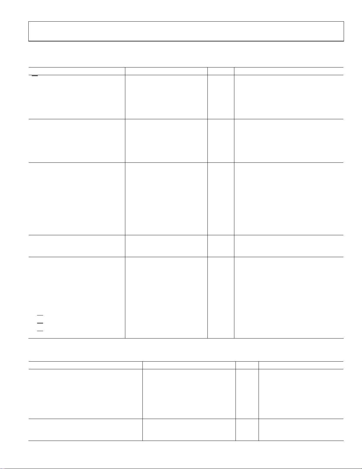
SERIAL PORT SPECIFICATIONS—SPI MODE
Table 17.
Parameter Min Typ Max Unit Test Conditions/Comments
CS
Input Logic 1 Voltage 2.0 V
Input Logic 0 Voltage 0.8 V
Input Logic 1 Current 30 µA
Input Logic 0 Current 110 µA
Input Capacitance 2 pF
SCLK Internal 30 kΩ pull-down resistor
Input Logic 1 Voltage 2.0 V
Input Logic 0 Voltage 0.8 V
Input Logic 1 Current 1 µA
Input Logic 0 Current 1 µA
Input Capacitance 2 pF
SDIO
As an Input
Input Logic 1 Voltage 2.0 V
Input Logic 0 Voltage 0.8 V
Input Logic 1 Current 1 µA
Input Logic 0 Current 1 µA
Input Capacitance 2 pF
As an Output
Output Logic 1 Voltage 2.7 V 1 mA load current
Output Logic 0 Voltage 0.4 V 1 mA load current
SDO
Output Logic 1 Voltage 2.7 V 1 mA load current
Output Logic 0 Voltage 0.4 V 1 mA load current
TIMING
SCLK
Clock Rate, 1/t
40 MHz
CLK
Pulse Width High, tHI 10 ns
Pulse Width Low, tLO 12 ns
SDIO to SCLK Setup, tDS 3 ns
SCLK to SDIO Hold, tDH 0 ns
SCLK to Valid SDIO and SDO, tDV 15 ns
CS to SCLK Setup (tS)
CS to SCLK Hold (tC)
CS Minimum Pulse Width High
Internal 30 kΩ pull-up resistor
10 ns
0 ns
6 ns
SERIAL PORT SPECIFICATIONS—I2C MODE
Table 18.
Parameter Min Typ Max Unit Test Conditions/Comments
SDA, SCL (AS INPUT) No internal pull-up/down resistor.
Input Logic 1 Voltage 0.7 × DVDD3 V
Input Logic 0 Voltage 0.3 × DVDD3 V
Input Current −10 +10 µA For VIN = 10% to 90% DVDD3
Hysteresis of Schmitt Trigger Inputs 0.015 × DVDD3
Pulse Width of Spikes That Must Be
Suppressed by the Input Filter, t
SP
SDA (AS OUTPUT)
Output Logic 0 Voltage 0.4 V IO = 3 mA.
Output Fall Time from V
IHmin
to V
20 + 0.1 C
ILmax
50 ns
1
250 ns 10 pF ≤ Cb ≤ 400 pF.
b
Rev. B | Page 11 of 112

AD9548
Parameter Min Typ Max Unit Test Conditions/Comments
TIMING
SCL Clock Rate 400 kHz
Bus-Free Time Between a Stop and Start
Condition, t
BUF
Repeated Start Condition Setup Time,
t
SU; STA
Repeated Hold Time Start Condition, t
Stop Condition Setup Time, t
SU; STO
HD; STA
0.6 µs
Low Period of the SCL Clock, tLO 1.3 µs
High Period of the SCL Clock, tHI 0.6 µs
SCL/SDA Rise Time, t
R
SCL/SDA Fall Time, tF 20 + 0.1 C
Data Setup Time, t
Data Hold Time, t
Capacitive Load for Each Bus Line, C
1
Cb is the capacitance (pF) of a single bus line.
100 ns
SU; DAT
100 ns
HD; DAT
1
400 pF
b
JITTER GENERATION
Table 19.
Parameter Min Typ Max Unit Test Conditions/Comments
JITTER GENERATION
f
= 1 Hz1; f
REF
Bandwidth: 100 Hz to 61 MHz 0.81 ps rms Random jitter
Bandwidth: 5 kHz to 20 MHz 0.73 ps rms Random jitter
Bandwidth: 20 kHz to 80 MHz 0.79 ps rms Random jitter
Bandwidth: 50 kHz to 80 MHz 0.78 ps rms Random jitter
Bandwidth: 4 MHz to 80 MHz 0.37 ps rms Random jitter
f
= 8 kHz1; f
REF
Bandwidth: 100 Hz to 77 MHz 0.71 ps rms Random jitter
Bandwidth: 5 kHz to 20 MHz 0.34 ps rms Random jitter
Bandwidth: 20 kHz to 80 MHz 0.43 ps rms Random jitter
Bandwidth: 50 kHz to 80 MHz 0.43 ps rms Random jitter
Bandwidth: 4 MHz to 80 MHz 0.31 ps rms Random jitter
f
= 19.44 MHz1; f
REF
Bandwidth: 100 Hz to 77 MHz 1.05 ps rms Random jitter
Bandwidth: 5 kHz to 20 MHz 0.34 ps rms Random jitter
Bandwidth: 20 kHz to 80 MHz 0.43 ps rms Random jitter
Bandwidth: 50 kHz to 80 MHz 0.43 ps rms Random jitter
Bandwidth: 4 MHz to 80 MHz 0.32 ps rms Random jitter
= 122.88 MHz2; f
DDS
= 155.52 MHz2; f
DDS
= 155.52 MHz2; f
DDS
= 0.01 Hz3
LOOP
= 100 Hz3
LOOP
LOOP
1.3 µs
0.6 µs
0.6 µs
20 + 0.1 C
1
300 ns
b
1
300 ns
b
= 20 MHz4 OCXO; fS = 1 GHz5; Q-
f
SYSCLK
divider = 1; default SysClk PLL charge pump
current; results valid for LVPECL, LVDS, and
CMOS output logic types
= 50 MHz4 crystal;
f
SYSCLK
= 1 GHz5; Q-divider = 1; default SYSCLK
f
S
PLL charge pump current; results valid for
LVPECL, LVDS, and CMOS output logic types
= 1 kHz3
= 50 MHz4 crystal;
f
SYSCLK
= 1 GHz5; Q-divider = 1; default SYSCLK
f
S
PLL charge pump current; results valid for
LVPECL, LVDS, and CMOS output logic types
After this period, the first clock
pulse is generated.
Rev. B | Page 12 of 112

AD9548
Parameter Min Typ Max Unit Test Conditions/Comments
f
= 19.44 Hz1; f
REF
Bandwidth: 100 Hz to 100 MHz 0.67 ps rms Random jitter
Bandwidth: 5 kHz to 20 MHz 0.31 ps rms Random jitter
Bandwidth: 20 kHz to 80 MHz 0.33 ps rms Random jitter
Bandwidth: 50 kHz to 80 MHz 0.33 ps rms Random jitter
Bandwidth: 4 MHz to 80 MHz 0.16 ps rms Random jitter
1
f
is the frequency of the active reference.
REF
2
f
is the output frequency of the DDS.
DDS
3
f
is the DPLL digital loop filter bandwidth.
LOOP
4
f
is the frequency at the SYSCLKP and SYSCLKN pins.
SYSCLK
5
fS is the sample rate of the output DAC.
= 311.04 MHz2; f
DDS
= 1 kHz3
LOOP
= 50 MHz4 crystal;
f
SYSCLK
= 1 GHz5; Q-divider = 1; default SYSCLK
f
S
PLL charge pump current; results valid for
LVPECL, LVDS, and CMOS output logic types
Rev. B | Page 13 of 112
AD9548
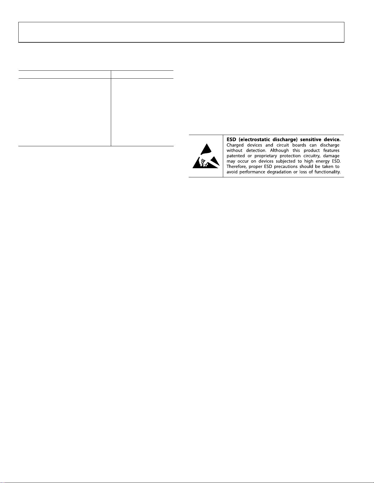
ABSOLUTE MAXIMUM RATINGS
Table 20.
Parameter Rating
Analog Supply Voltage (AVDD) 2 V
Digital Supply Voltage (DVDD) 2 V
Digital I/O Supply Voltage (DVDD3) 3.6 V
DAC Supply Voltage (AVDD3) 3.6 V
Maximum Digital Input Voltage −0.5 V to DVDD3 + 0.5 V
Storage Temperature Range −65°C to +150°C
Operating Temperature Range −40°C to +85°C
Lead Temperature (Soldering 10 sec) 300°C
Junction Temperature 150°C
Stresses above those listed under Absolute Maximum Ratings
may cause permanent damage to the device. This is a stress
rating only; functional operation of the device at these or any
other conditions above those indicated in the operational
section of this specification is not implied. Exposure to absolute
maximum rating conditions for extended periods may affect
device reliability.
ESD CAUTION
Rev. B | Page 14 of 112
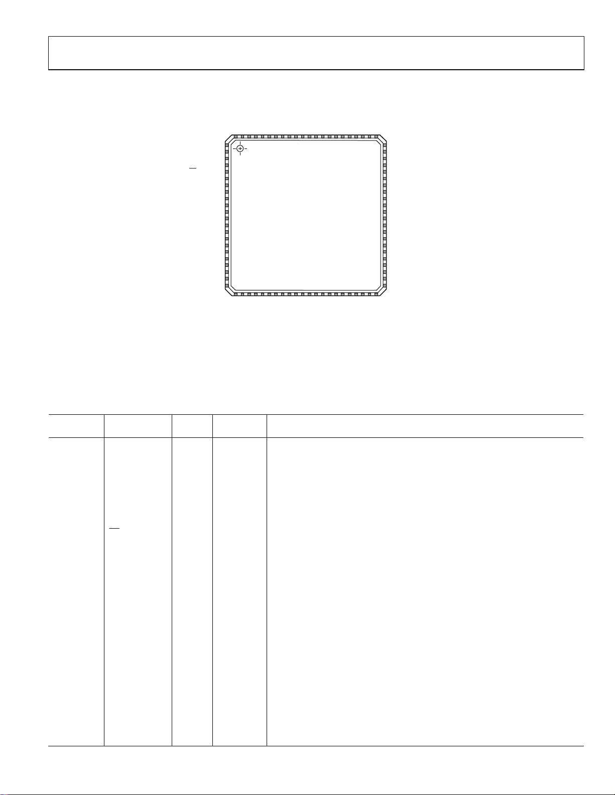
AD9548
PIN CONFIGURATION AND FUNCTION DESCRIPTIONS
M7M6M5M4DVDD
DVDD
88
DVDD
SDIO
SDO
DVDD
DVDD3
TCLK
TMS
TDO
TDI
DVDD
RESET
DVDD
DVDD
NC
1
2
3
4
5
6
7
8
9
10
11
12
13
14
15
16
17VSS
18DACOUTP
19DACOUTN
20VSS
21AVDD3
22AVDD3
232425262728293031323334363735
AVDD
AVDD
SCLK/SCL
CS/SDA
NOTES
1. NC = NO CONNECT .
2. THE EXPO SED PAD MUST BE CONNECTED TO GROUND (VSS ).
DVDD3
M3M2M1
798081828384858687
AD9548
TOP VIEW
(Not to Scale)
88-LEAD LFCSP
12mm × 12mm
0.5mm PIT CH
VSS
VSS
AVDD
OUT0P
AVDD3
CLKINP
CLKINN
OUT_RSET
AVDD
AVDD3
REFDD
383940
OUT2P
AVDD3
AVDD
REFCC
REFD
41
424344
AVDD
OUT3P
OUT2N
DVDD
IRQNCAVDD3
M0
7877767574737271706968
AVDD
OUT1P
OUT1N
OUT0N
REFC
AVDD3
67
OUT3N
AVDD3
66
AVDD3
65
REFBB
64
REFB
AVDD
63
62
REFAA
61
REFA
AVDD3
60
AVDD
59
58
TDC_VRT
57
TDC_VRB
NC
56
AVDD
55
VSS
54
SYSCLKP
53
SYSCLKN
52
VSS
51
AVDD
50
SYSCLK_LF
49
SYSCLK_VREG
48
AVDD3
47
46
NC
45
NC
08022-002
Figure 2. 88-Lead LFCSP Pin Configuration
Table 21. Pin Function Descriptions
Input/
Pin No. Mnemonic
1, 6, 12, 77,
DVDD I Power 1.8 V Digital Supply.
Output
Pin Type Description
83, 88
2 SCLK/SCL I 3.3 V CMOS Serial Programming Clock. Data clock for serial programming.
3 SDIO I/O 3.3 V CMOS
Serial Data Input/Output. When the device is in 4-wire mode, data is written via
this pin. In 3-wire mode, both data reads and writes occur on this pin. There is no
internal pull-up/pull-down resistor on this pin.
4 SDO O 3.3 V CMOS
Serial Data Output. Use this pin to read data in 4-wire mode (high impedance in
3-wire mode). There is no internal pull-up/pull-down resistor on this pin.
5
CS
/SDA
I 3.3 V CMOS
Chip Select (SPI). Active low. When programming a device, this pin must be held
low. In systems where more than one AD9548 is present, this pin enables
individual programming of each AD9548 (in I
2
C® mode, this is a serial data pin).
This pin has an internal 10 kΩ pull-up resistor but only in SPI mode.
7, 82 DVDD3 I Power 3.3 V I/O Digital Supply.
8 TCLK I JTAG Clock. Internal pull-down resistor; no connection if JTAG is not used.
9 TMS I JTAG Mode. Internal pull-up resistor; no connection if JTAG is not used.
10 TDO O JTAG Output. No connection if JTAG is not used
11 TDI I JTAG Input. Internal pull-up resistor; no connection if JTAG is not used.
13 RESET I 3.3 V CMOS
Chip Reset. When this active high pin is asserted, the chip goes into reset.
This pin has an internal 50 kΩ pull-down resistor.
14, 15 DVDD I Power 1.8 V DAC Decode Digital Supply. Keep isolated from the 1.8 V core digital supply.
16, 45, 46 NC No Connect.
17, 20, 25,
VSS O Ground Analog Ground. Connect to ground.
28, 51, 54
18 DACOUTP O
Differential
DAC Output. DACOUTP contains an internal 50 Ω pull-down resistor.
output
19 DACOUTN O
Differential
output
Complementary DAC Output. DACOUTN contains an internal 50 Ω pull-down
resistor.
Rev. B | Page 15 of 112
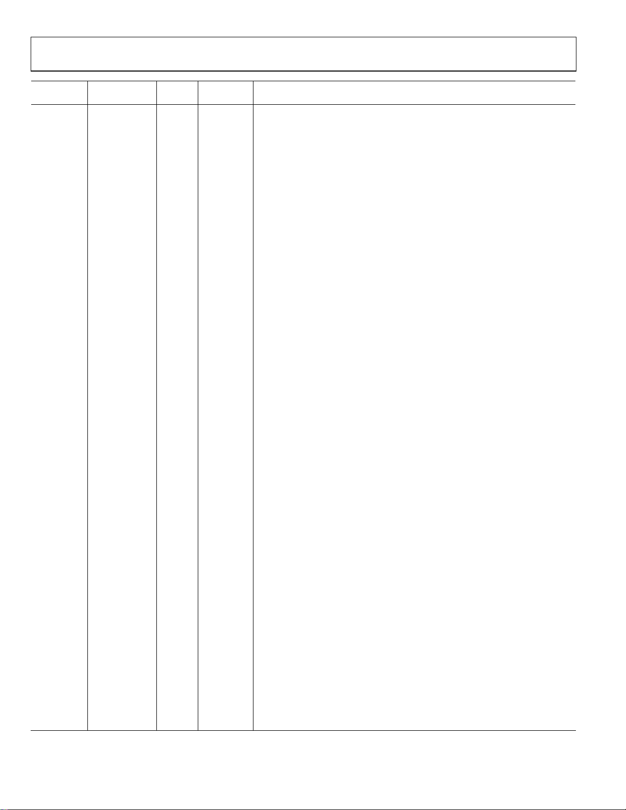
AD9548
Input/
Pin No. Mnemonic
21, 22 AVDD3 I Power 3.3 V Analog (DAC) Power Supply.
23, 24 AVDD I Power 1.8 V Analog (DAC) Power Supply.
26 CLKINN I
27 CLKINP I
29 AVDD I Power 1.8 V Analog (Input Receiver) Power Supply.
30 OUT_RSET O
31, 37, 38,
44
32 OUT0P O
33 OUT0N O
34, 41 AVDD I Power 1.8 V Analog (Output Divider) Power Supply.
35 OUT1P O
36 OUT1N O
39 OUT2P O
40 OUT2N O
42 OUT3P O
43 OUT3N O
47 AVDD3 I Power 3.3 V Analog (System Clock) Power Supply.
48 SYSCLK_VREG I
49 SYSCLK_LF O
50, 55 AVDD I Power 1.8 V Analog (System Clock) Power Supply.
52 SYSCLKN I
AVDD3 I Power
Output Pin Type Description
Differential
input
Differential
input
Current set
resistor
LVPECL,
LVDS, or
CMOS
LVPECL,
LVDS, or
CMOS
LVPECL,
LVDS, or
CMOS
LVPECL,
LVDS, or
CMOS
LVPECL,
LVDS, or
CMOS
LVPECL,
LVDS, or
CMOS
LVPECL,
LVDS, or
CMOS
LVPECL,
LVDS, or
CMOS
Differential
input
Clock Distribution Input. In standard operating mode, this pin is connected to the
filtered DACOUTN output. This internally biased input is typically ac-coupled and,
when configured as such, can accept any differential signal whose single-ended
swing is at least 400 mV.
Clock Distribution Input. In standard operating mode, this pin is connected to the
filtered DACOUTP output
Connect an optional 3.12 kΩ resistor from this pin to ground (see the Output
Current Control with an External Resistor section).
Analog Supply for Output Driver. These pins are normally 3.3 V but can be 1.8 V.
Pin 31 powers Out0x. Pin 37 powers OUT1x. Pin 38 powers OUT2x. Pin 44 powers
OUT3x. Apply power to these pins even if the corresponding outputs (OUT0P/
OUT0N, OUT1P/ OUT1N, OUT2P/ OUT2N, and OUT3P/ OUT3N) are not used. See
the Power Supply Partitions section.
Output 0. This output can be configured as LVPECL, LVDS, or single-ended CMOS.
LVPECL and LVDS operation require a 3.3 V output driver power supply. CMOS
operation can be either 1.8 V or 3.3 V, depending on the output driver power
supply.
Complementary Output 0. This output can be configured as LVPECL, LVDS, or
single-ended CMOS.
Output 1. This output can be configured as LVPECL, LVDS, or single-ended CMOS.
LVPECL and LVDS operation require a 3.3 V output driver power supply. CMOS
operation can be either 1.8 V or 3.3 V, depending on the output driver power
supply.
Complementary Output 1. This output can be configured as LVPECL, LVDS, or
single-ended CMOS.
Output 2. This output can be configured as LVPECL, LVDS, or single-ended CMOS.
LVPECL and LVDS operation require a 3.3 V output driver power supply. CMOS
operation can be either 1.8 V or 3.3 V, depending on the output driver power
supply.
Complementary Output 2. This output can be configured as LVPECL, LVDS, or
single-ended CMOS.
Output 3. This output can be configured as LVPECL, LVDS, or single-ended CMOS.
LVPECL and LVDS operation require a 3.3 V output driver power supply. CMOS
operation can be either 1.8 V or 3.3 V, depending on the output driver power
supply.
Complementary Output 3. This output can be configured as LVPECL, LVDS, or
single-ended CMOS.
System Clock Loop Filter Voltage Regulator. Connect a 0.1 F capacitor from this
pin to ground. This pin is also the ac ground reference for the integrated SYSCLK
PLL multiplier’s external loop filter (see the SYSCLK PLL Multiplier section).
System Clock Multiplier Loop Filter. When using the frequency multiplier to drive
the system clock, an external loop filter can be attached to this pin.
Complementary System Clock Input. Complementary signal to SYSCLKP. SYSCLKN
contains internal dc biasing and should be ac-coupled with a 0.01 F capacitor,
except when using a crystal, in which case connect the crystal across SYSCLKP
and SYSCLKN.
Rev. B | Page 16 of 112

AD9548
Input/
Pin No. Mnemonic
53 SYSCLKP I
56, 75 NC I No Connection. These pins should be left floating.
59 AVDD I Power 1.8 V Analog Power Supply.
57, 58
60, 66, 67,
73
61 REFA I
62 REFAA I
63, 70, 74 AVDD I Power 1.8 V Analog (Reference Input) Power Supply.
64 REFB I
65 REFBB I
68 REFC I
69 REFCC I
71 REFD I
72 REFDD I
76 IRQ O Logic Interrupt Request Line.
78, 79, 80,
81, 84, 85,
86, 87
EP VSS O
TDC_VRB,
TDC_VRT
AVDD3 I Power 3.3 V Analog (Reference Input) Power Supply.
M0, M1, M2,
M3, M4, M5,
M6, M7
Output Pin Type Description
Differential
input
I Use capacitive decoupling on these pins (see Figure 38).
Differential
input
Differential
input
Differential
input
Differential
input
Differential
input
Differential
input
Differential
input
Differential
input
I/O 3.3 V CMOS Configurable I/O Pins. These pins are configured under program control.
Exposed
pad
System Clock Input. SYSCLKP contains internal dc biasing and should be ac-
coupled with a 0.01 F capacitor, except when using a crystal, in which case
connect the crystal across SYSCLKP and SYSCLKN. Single-ended 1.8 V CMOS is
also an option but can introduce a spur if the duty cycle is not 50%. When using
SYSCLKP as a single-ended input, connect a 0.01 F capacitor from SYSCLKN to
ground.
Reference A Input. This internally biased input is typically ac-coupled and, when
configured as such, can accept any differential signal with single-ended swing up
to 3.3 V. If dc-coupled, input can be LVPECL, CMOS, or LVDS.
Complementary Reference A Input. Complementary signal to the input provided
on Pin 61. The user can configure this pin as a separate single-ended input.
Reference B Input. This internally biased input is typically ac-coupled and, when
configured as such, can accept any differential signal with single-ended swing up
to 3.3 V. If dc-coupled, input can be LVPECL, CMOS, or LVDS.
Complementary Reference B Input. Complementary signal to the input provided
on Pin 64. The user can configure this pin as a separate single-ended input.
Reference C Input. This internally biased input is typically ac-coupled and, when
configured as such, can accept any differential signal with single-ended swing up
to 3.3 V. If dc-coupled, input can be LVPECL, CMOS, or LVDS.
Complementary Reference C Input. Complementary signal to the input provided
on Pin 68. The user can configure this pin as a separate single-ended input.
Reference D Input. This internally biased input is typically ac-coupled and, when
configured as such, can accept any differential signal with single-ended swing up
to 3.3 V. If dc-coupled, input can be LVPECL, CMOS, or LVDS.
Complementary Reference D Input. Complementary signal to the input provided
on Pin 71. The user can configure this pin as a separate single-ended input.
The exposed pad must be connected to ground (VSS).
Rev. B | Page 17 of 112
AD9548
–
–
–
–
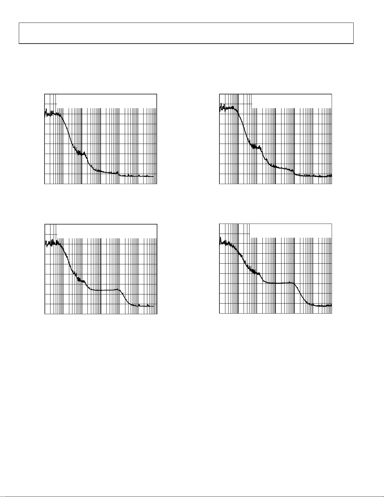
TYPICAL PERFORMANCE CHARACTERISTICS
fR = input reference clock frequency; fO = clock frequency; f
loop bandwidth; PLL off = SYSCLK PLL bypassed; PLL on = SYSCLK PLL enabled; I
PLL loop filter. AVDD, AVDD3, and DVDD at nominal supply voltage, f
–100
–120
–130
PHASE NOISE (dBc/Hz)
–140
–150
–160
PHASE NOISE ( dBc/Hz)
70
–80
–90
–110
70
–80
–90
–100
–110
–120
–130
–140
–150
–160
INTEGRATED RMS JITTER (PHASE NOISE):
5kHz TO 20MHz: 173fs (–75.4d Bc)
20kHz TO 80MHz: 315fs (–70.2d Bc) (EXTRAPO LATED)
100 1k 10k 100k 1M 10M 100M
FREQUENCY O FFSET (Hz)
Figure 3. Additive Phase Noise (Output Driver = LVPECL),
f
= 19.44 MHz, fO = 155.52 MHz,
R
LBW = 1 kHz, f
INTEGRATED RMS JITTER (PHASE NOISE):
5kHz TO 20MHz: 333fs (–69.8d Bc)
20kHz TO 80MHz: 430fs (–67.6dBc) (EXTRAPO LATED)
100 1k 10k 100k 1M 10M 100M
FREQUENCY OFFSET (Hz)
= 1 GHz, PLL Off
SYS
Figure 4. Additive Phase Noise (Output Driver = LVPECL),
f
= 19.44 MHz, fO = 155.52 MHz,
R
LBW = 1 kHz, f
= 50 MHz (Crystal), PLL On
SYS
= SYSCLK input frequency; fS = internal system clock frequency; LBW = DPLL
SYS
= 1 GHz, ICP = automatic mode, LF = internal, unless otherwise noted.
S
70
–80
–90
–100
–110
–120
–130
PHASE NOISE (dBc/Hz)
–140
–150
–160
08022-068
70
–80
–90
–100
–110
–120
–130
PHASE NOISE (dBc/Hz)
–140
–150
–160
08022-056
= SYSCLK PLL charge pump current; LF = SYSCLK
CP
INTEGRATED RMS JITTER (PHASE NOISE):
5kHz TO 20MHz: 103fs (–74.0dBc)
20kHz TO 80MHz: 160fs (–70.1dBc)
100 1k 10k 100k 1M 10M 100M
FREQUENCY OFFSET (Hz)
Figure 5. Additive Phase Noise (Output Driver = LVPECL),
f
= 19.44 MHz, fO = 311.04 MHz,
R
LBW = 1 kHz, f
INTEGRATED RMS JITTER (PHASE NOISE):
5kHz TO 20MHz: 310fs (–64.4dBc)
20kHz TO 80MHz: 330fs (–63.9d Bc)
100 1k 10k 100k 1M 10M 100M
FREQUENCY OFFSET (Hz)
= 1 GHz, PLL Off
SYS
Figure 6. Additive Phase Noise (Output Driver = LVPECL),
= 19.44 MHz, fO = 311.04 MHz,
f
R
LBW = 1 kHz, f
= 50 MHz (Crystal), PLL On
SYS
08022-066
08022-067
Rev. B | Page 18 of 112
AD9548
–
–
–
–
–
–
PHASE NOISE (dBc/Hz)
70
–80
–90
–100
–110
–120
–130
–140
–150
–160
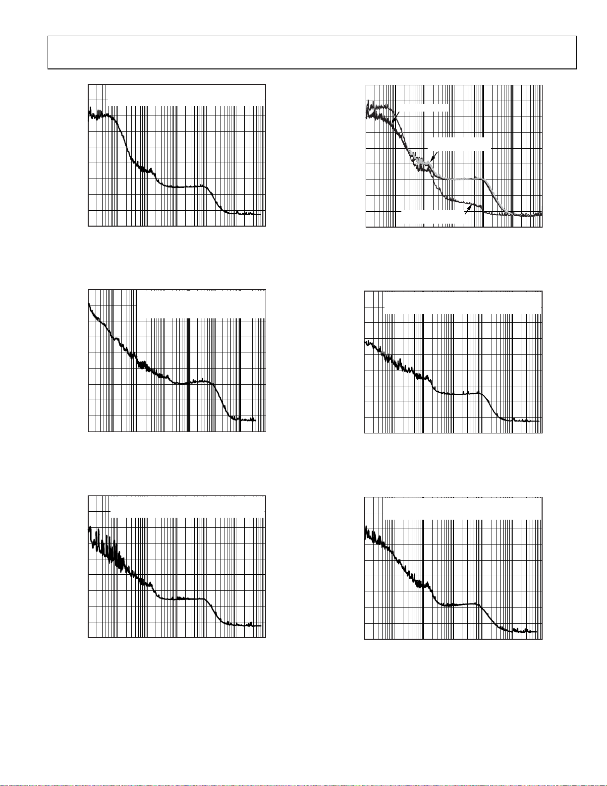
INTEGRATED RMS JITTER (PHASE NOISE):
5kHz TO 20MHz: 361fs (–69.0d Bc)
20kHz TO 80MHz: 441fs (–67.3d Bc) (EXTRAPO LATED)
100 1k 10k 100k 1M 10M 100M
FREQUENCY O FFSET (Hz)
Figure 7. Additive Phase Noise (Output Driver = LVPECL),
= 19.44 MHz, fO = 155.52 MHz,
f
R
LBW = 1 kHz, f
70
–80
–90
–100
–110
–120
–130
PHASE NOISE (dBc/Hz)
–140
–150
–160
10 100 1k 10k 100k 1M 10M 100M
INTEGRATED RMS JITTER (PHASE NOISE):
5kHz TO 10MHz: 717fs (–65.1d Bc)
12kHz TO 20MHz: 725fs (–65.0dBc)
20kHz TO 80MHz: 790fs (–64.3dBc)
FREQUENCY O FFSET (Hz)
= 50 MHz, PLL On
SYS
Figure 8. Additive Phase Noise (Output Driver = LVPECL),
= 1 Hz, fO = 122.88 MHz,
f
LBW = 0.05 Hz, f
70
–80
–90
–100
–110
–120
–130
PHASE NOISE ( dBc/Hz)
–140
–150
–160
100 1k 10k 100k 1M 10M 100M
R
= 20 MHz (OCXO), PLL On
SYS
INTEGRAT ED RMS JITT ER (PHASE NOI SE):
5kHz TO 20MHz : 336fs (–69.7d Bc)
20kHz TO 80MHz : 425fs (–67.6d Bc) (EXTRAP OLATED)
FREQUENCY O FFSET (Hz)
Figure 9. Additive Phase Noise (Output Driver = LVPECL),
= 8 kHz, fO = 155.52 MHz,
f
R
LBW = 100 Hz, f
= 50 MHz (Crystal), PLL On
SYS
08022-069
08022-044
08022-052
70
–80
–90
–100
–110
–120
–130
PHASE NOISE ( dBc/Hz)
–140
–150
–160
100 1k 10k 100k 1M 10M 100M
50MHz CRYSTAL
ROHDE & SCHWARZ
SMA100 (50MHz)
ROHDE & SCHWARZ
SMA100 (1GHz)
FREQUENCY ( Hz)
Figure 10. Additive Phase Noise Comparison of SYSCLK Input Options
(Output Driver = LVPECL),
= 19.44 MHz, fO = 311.04 MHz, LBW = 1 kHz
f
R
–100
–110
–120
–130
PHASE NOISE (dBc/Hz)
–140
–150
–160
70
–80
–90
INTEGRATED RMS JITTER (PHASE NOISE):
5kHz TO 20MHz: 356fs (–69.2dBc)
20kHz TO 80MHz: 435fs (–67.4dBc) (EXTRAPO LATED)
100 1k 10k 100k 1M 10M 100M
FREQUENCY O FFSET (Hz)
Figure 11. Additive Phase Noise (Output Driver = LVPECL),
= 1 Hz, fO = 155.52 MHz,
f
R
LBW = 0.05 Hz, f
–100
–110
–120
–130
PHASE NOISE ( dBc/Hz)
–140
–150
–160
70
–80
–90
INTEGRATED RMS JITTER (PHASE NOISE):
5kHz TO 20MHz: 245fs (–72.4d Bc)
20kHz TO 80MHz: 300fs (–64.3dBc) (EXTRAPO LATED)
100 1k 10k 100k 1M 10M 100M
FREQUENCY O FFSET (Hz)
= 50 MHz, PLL On
SYS
Figure 12. Additive Phase Noise (Output Driver = LVPECL) ,
= 19.44 MHz, fO = 155.52 MHz,
f
R
LBW = 1 kHz, f
2x Frequency Multiplier, I
= 50 MHz (Crystal), PLL On with
SYS
= 375 μA, LF = External (350 kHz)
CP
08022-058
08022-054
08022-051
Rev. B | Page 19 of 112
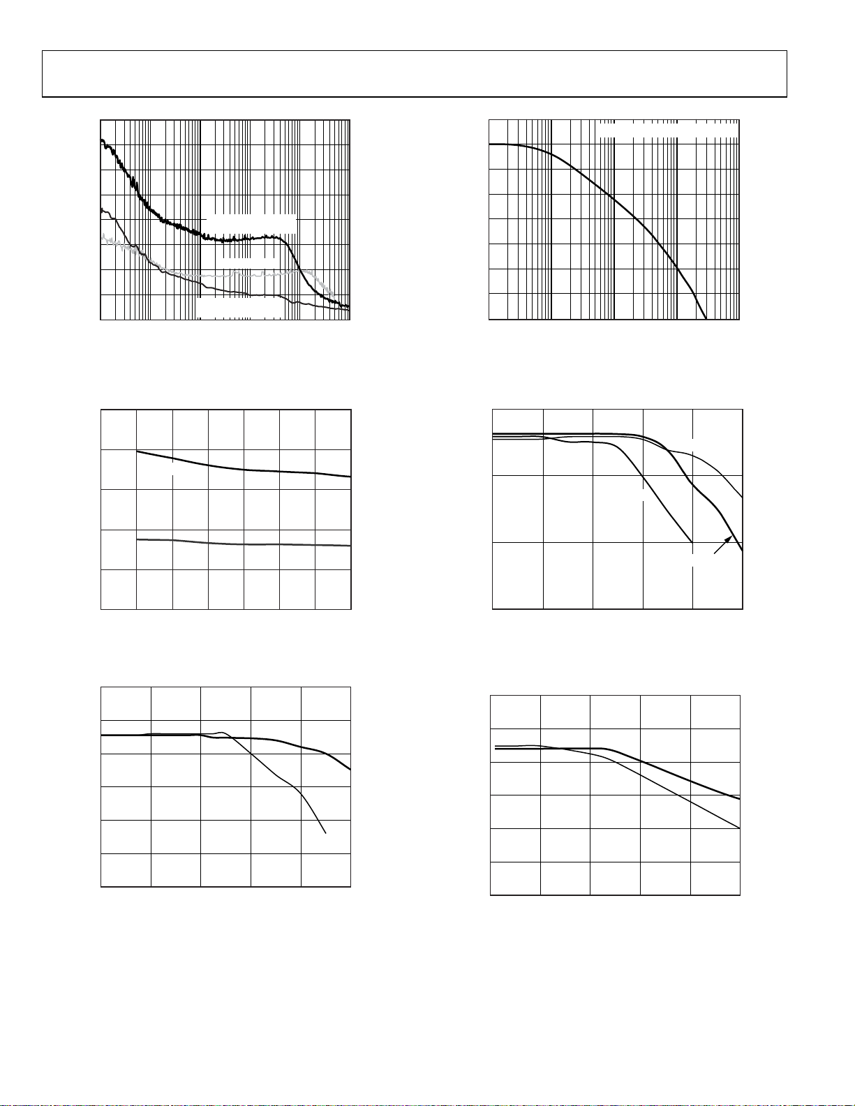
AD9548
–
90
–100
10
CLOSED-LOOP PEAKING: 0.04dB
0
–110
–120
–130
–140
PHASE NOISE ( dBc/Hz)
–150
–160
–170
100 1k 10k 100k 1M 10M
ROHDE & SCHW ARZ
SMA100 (1GHz)
20MHz OCXO
ROHDE & SCHWARZ
SMA100 (50MHz)
FREQUENCY OFFSET (Hz)
Figure 13. Phase Noise of SYSCLK Input Sources
1.0
0.8
LVPECL
0.6
0.4
AMPLITUDE (V)
0.2
LVDS
–10
–20
–30
–40
CLOSED-LOOP GAIN (dB)
–50
–60
–70
10 100 1k 10k 100k
08022-053
FREQUENCY OFFSET (Hz)
08022-047
Figure 16. Jitter Transfer Bandwidth, Output Driver = LVPECL,
= 19.44 MHz, fO = 155.52 MHz,
f
LBW = 100 Hz (Phase Margin = 88°), f
R
2.0
1.5
AMPLITUDE (V)
1.0
20pF LOAD
= 1 GHz, PLL Off
SYS
5pF LOAD
10pF LOAD
0
0 100 200 300 400 500 600 700
FREQUENCY ( MHz)
Figure 14. Amplitude vs. Toggle Rate,
LVPECL and LVDS
4.0
3.5
3.0
2.5
AMPLITUDE (V)
2.0
1.5
1.0
0 100 200 300 400 500
FREQUE NCY (MHz)
10pF LO AD
20pF LOAD
Figure 15. Amplitude vs. Toggle Rate,
3.3 V CMOS (Strong Mode)
0.5
0 50 100 150 250200
08022-049
FREQUENCY (MHz)
08022-062
Figure 17. Amplitude vs. Toggle Rate,
1.8 V CMOS
4.0
3.5
3.0
2.5
AMPLITUDE (V)
2.0
1.5
1.0
08022-055
0 1020304050
5pF LOAD
10pF LOAD
FREQUE NCY (MHz)
08022-063
Figure 18. Amplitude vs. Toggle Rate,
3.3 V CMOS (Weak Mode)
Rev. B | Page 20 of 112
AD9548
A
140
130
120
110
100
90
POWER (mW)
80
70
60
50
0 100 200 300 400 500
LVPECL
LVDS
FREQUE NCY (MHz)
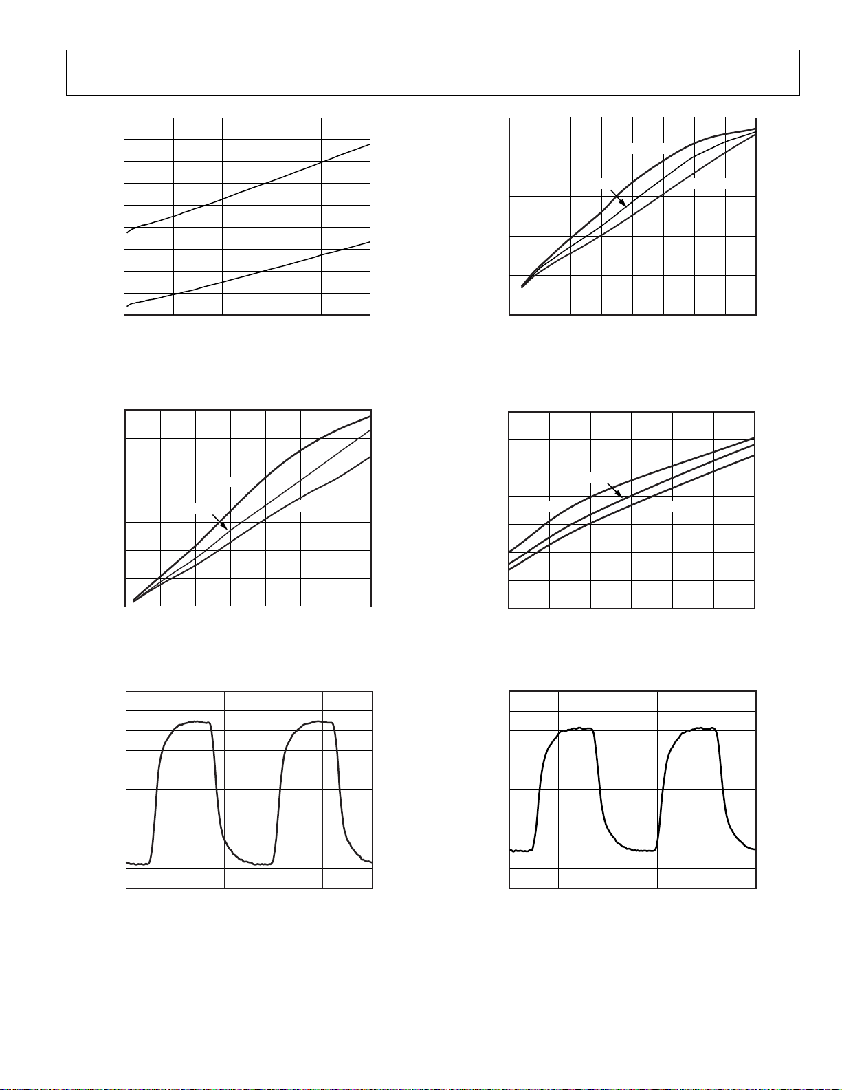
Figure 19. Power Consumption vs. Frequency,
LVPECL and LVDS
(Single Channel)
160
08022-064
40
35
30
25
POWER (mW)
20
15
0 50 100 150 200
10pF LOAD
20pF LO AD
5pF LOAD
FREQUENCY (MHz)
Figure 22. Power Consumption vs. Frequency,
1.8 V CMOS
34
08022-061
140
120
10pF LOAD
20pF LO AD
5pF LOAD
FREQUENCY (M Hz)
100
80
POWER (mW)
60
40
20
0 50 100 1 50 200 250 300 350
Figure 20. Power Consumption vs. Frequency,
3.3 V CMOS (Strong Mode)
1.0
0.8
0.6
0.4
0.2
0
–0.2
–0.4
DIFFERENTIAL AMPLITUDE (V)
–0.6
–0.8
–1.0
012345
TIME (ns)
Figure 21. Output Waveform,
LVPECL (400 MHz)
32
30
28
20pF LOAD 5p F LOAD
26
POWER (mW)
24
22
20
10 15 20 25 30 35 40
08022-060
10pF LOAD
FREQUENCY (MHz)
08022-059
Figure 23. Power Consumption vs. Frequency,
3.3 V CMOS (Weak Mode)
0.5
0.4
0.3
0.2
0.1
0
L AMPLITUDE (V)
–0.1
–0.2
DIFFERENTI
–0.3
–0.4
–0.5
012345
08022-050
TIME (ns)
08022-048
Figure 24. Output Waveform,
LVDS (400 MHz)
Rev. B | Page 21 of 112
AD9548
3.5
3.0
2.5
20pF LOAD
10pF LOAD
3.5
3.0
2.5
5pF LO AD
AMPLITUDE (V)
2.0
1.5
1.0
0.5
0
–0.5
20 pF LOAD
0 1020304050607080
TIME (ns)
08022-046
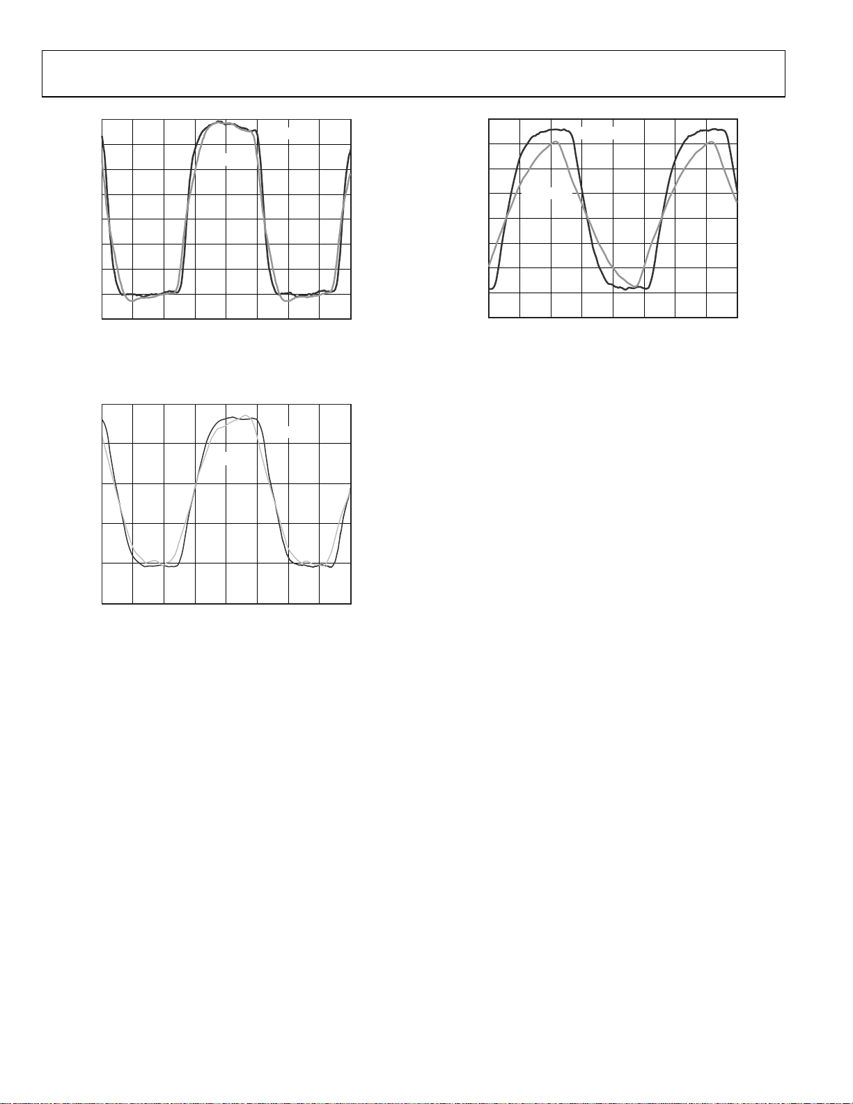
Figure 27. Output Waveform,
3.3 V CMOS (20 MHz, Weak Mode)
2.0
1.5
1.0
AMPLITUDE ( V)
0.5
0
–0.5
0 2 4 6 8 10 12 14 16
TIME (ns)
Figure 25. Output Waveform,
3.3 V CMOS (100 MHz, Strong Mode)
2.0
1.5
20pF LOAD
1.0
10pF LOAD
08022-057
0.5
AMPLITUDE (V)
0
–0.5
0 2 4 6 8 10 12 14 16
TIME (ns)
Figure 26. Output Waveform,
1.8 V CMOS (100 MHz)
08022-065
Rev. B | Page 22 of 112
AD9548
INPUT/OUTPUT TERMINATION RECOMMENDATIONS
0.1µF
AD9548
3.3V LVDS
OUTPUT
100Ω
IMPEDANCE
0.1µF
HIGH
INPUT
DOWNST REAM
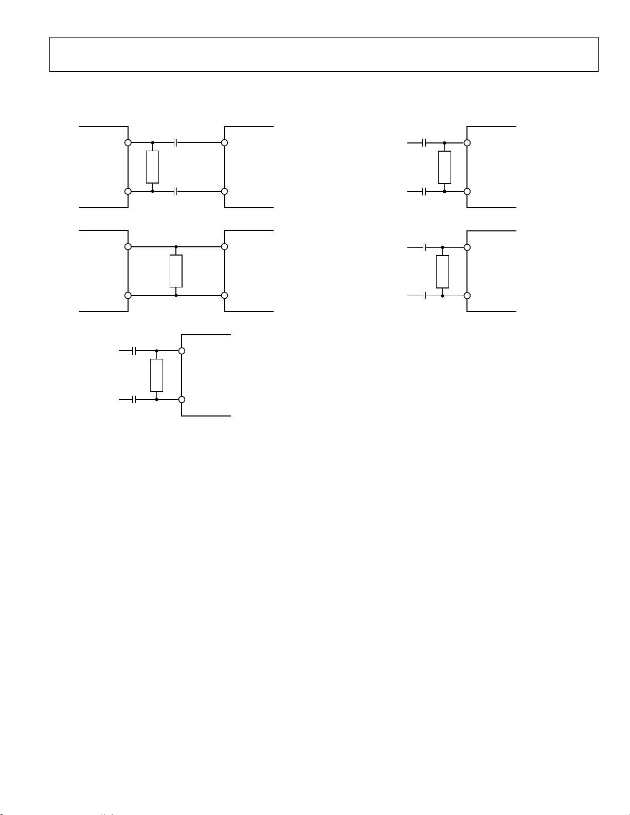
Figure 28. AC-Coupled LVDS or LVPECL Output Driver
AD9548
3.3V
LVPECL-
COMPATIBL E
OUTPUT
100Ω
DOWNST REAM
Figure 29. DC-Coupled LVDS or LVPECL Output Driver
0.1µF
AD9548
(OPTIO NAL)
SELF-BIASED
REFERENCE
INPUT
0.1µF
100Ω
Figure 30. Reference Input
DEVICE
DEVICE
08022-005
0.1µF
AD9548
SELF-BIASED
0.1µF
08022-003
100Ω
SYSCLK
INPUT
(OPTIO NAL)
08022-006
Figure 31. SYSCLKx Input
0.1µF
AD9548
(OPTIO NAL)
SELF-BIASED
CLKINx
INPUT
08022-007
100Ω
0.1µF
08022-004
Figure 32. CLKINx Input
Rev. B | Page 23 of 112

AD9548
GETTING STARTED
POWER-ON RESET
The AD9548 monitors the voltage on the power supplies at
power-up. When DVDD3 is greater than 2.35 V ± 0.1 V and
DVDD (Pin 1, Pin 6, Pin 12, Pin 77, Pin 83, and Pin 88) is
greater than 1.4 V ± 0.05 V, the device generates a 75 ns reset
pulse. The power-up reset pulse is internal and independent of
the RESET pin. This internal power-up reset sequence eliminates
the need for the user to provide external power supply sequencing.
Within 45 ns after the leading edge of the internal reset pulse,
the M0 to M7 multifunction pins behave as high impedance
digital inputs and remain so until programmed otherwise.
INITIAL PIN PROGRAMMING
During a device reset (either via the power-up reset pulse or the
RESET pin), the multifunction pins (M0 to M7) behave as high
impedance inputs, but upon removal of the reset condition,
level-sensitive latches capture the logic pattern present on the
multifunction pins. The AD9548 requires that the user supply
the desired logic state to the M0 to M7 pins by means of pull-up
and/or pull-down resistors (nominally 10 k to 30 k).
The initial state of the M0 to M7 pins following a reset is
referred to as FncInit, Bits[7:0]. Bits[7:0] of FncInit map directly
to the logic states of M7:0, respectively. The three LSBs of
FncInit (FncInit, Bits[2:0]) determine whether the serial port
interface behaves according to the SPI or I
Specifically, FncInit, Bits[2:0] = 000 selects the SPI interface,
while any other value selects the I
2
the I
C bus address set to the value of FncInit, Bits[2:0].
The five MSBs of FncInit (FncInit, Bits[7:3]) determine the
operation of the EEPROM loader. On the falling edge of RESET,
if FncInit, Bits[7:3] = 00000, then the EEPROM contents are not
transferred to the control registers and the device registers
assume their default values. However, if FncInit, Bits[7:3] ≠
00000, then the EEPROM controller transfers the contents of
the EEPROM to the control registers with condition = FncInit,
Bits[7:3] (see the EEPROM section).
2
DEVICE REGISTER PROGRAMMING
The initial state of the M0 to M7 pins establishes the serial I/O
port protocol (SPI or I
protocol, and assuming that an EEPROM download is not used,
program the device according to the recommended sequence
described in the Program the System Clock Functionality
section through the Generate the Output Clock section.
Program the System Clock Functionality
The system clock parameters reside in the 0100 register address
space. They include the following:
• System clock PLL controls
• System clock period
• System clock stability timer
2
C). Using the appropriate serial port
2
C protocol.
C port with the three LSBs of
Rev. B | Page 24 of 112
It is essential to program the system clock period because many of
the AD9548 subsystems rely on this value. It is highly recommended
to program the system clock stability timer, as well. This is
especially important when using the system clock PLL but also
applies if using an external system clock source, especially if the
external source is not expected to be completely stable when
power is applied to the AD9548.
Initialize the System Clock
After the system clock functionality is programmed, issue an
I/O update using Register 0005, Bit 0 to invoke the system clock
settings.
Calibrate the System Clock (Only if Using SYSCLK PLL)
Set the calibrate system clock bit in the sync/cal register
(Address 0A02, Bit 0) and issue an I/O update. Then clear the
calibrate system clock bit and issue another I/O update. This
action allows time for the calibration to proceed while programming the remaining device registers.
Program the Multifunction Pins (Optional)
This step is required only if the user intends to use any of the
multifunction pins for status or control. The multifunction pin
parameters reside in the 0200 to 0207 register address space.
The default configuration of the multifunction pins is as an
undesignated high impedance input pin.
Program the IRQ Functionality (Optional)
This step is required only if the user intends to use the IRQ feature.
IRQ control resides in the 0200 to 0207 register address space. It
includes the following:
• IRQ pin mode control
• IRQ mask
The IRQ mask default values prevent interrupts from being
generated. The IRQ pin mode default is open-drain NMOS.
Program the Watchdog Timer (Optional)
This step is required only if the user intends to use it. Watchdog
timer control resides in the 0200 register address space. The
watchdog timer is disabled by default.
Program the DAC Full-Scale Current (Optional)
This step is required only if the user intends to use a full-scale
current setting other than the default value. DAC full-scale
current control resides in the 0200 register address space.
Program the Digital Phase-Locked Loop (DPLL)
The DPLL parameters reside in the 0300 register address space.
They include the following:
• Free-run frequency (DDS frequency tuning word)
• DDS phase offset
• DPLL pull-in range limits
• DPLL closed-loop phase offset
• Phase slew control (for hitless reference switching)
• Tuning word history control (for holdover operation)

AD9548
Program the Clock Distribution Outputs
The clock distribution parameters reside in the 0400 register
address space. They include the following:
• Output power-down control
• Output enable (disabled by default)
• Output synchronization
• Output mode control
• Output divider functionality
Program the Reference Inputs
The reference input parameters reside in the 0500 register
address space. They include the following:
• Reference power-down
• Reference logic family
• Reference profile assignment control
• Phase build-out control
Program the Reference Profiles
The reference profile parameters reside in the 0600 to 0700
register address space. They include the following:
• Reference priority
• Reference period
• Reference period tolerance
• Reference validation timer
• Reference redetect timer
• Digital loop-filter coefficients
• Reference prescaler (R-divider)
• Feedback dividers (S, U, and V)
• Phase and frequency lock detector controls
Generate the Reference Acquisition
After the registers are programmed, issue an I/O update using
Register 0005, Bit 0 to invoke all of the register settings
programmed up to this point.
If the settings are programmed for manual profile assignment,
the DPLL locks to the first available reference that has the
highest priority. If the settings are programmed for automatic
profile assignment, then write to the reference profile detect
register (Address 0A0D) to select the state machines that
require starting. Next, issue an I/O update (Address 0005, Bit 0)
to start the selected state machines. Upon completion of the
reference detection sequence, the DPLL locks to the first
available reference with the highest priority.
Generate the Output Clock
If the registers are programmed for automatic clock distribution
synchronization via DPLL phase or frequency lock, the synthesized output signal appears at the clock distribution outputs
(assuming the output is enabled and that the DDS output signal
has been routed to the CLKIN input pins). Otherwise, set and
then clear the sync distribution bit (Address 0A02, Bit 1) or use
a multifunction pin input (if programmed accordingly) to generate
a clock distribution sync pulse, which causes the synthesized
output signal to appear at the clock distribution outputs.
Rev. B | Page 25 of 112
AD9548
THEORY OF OPERATION
REFA
REFAA
REFB
REFBB
REFC
REFCC
REFD
REFDD
M0 TO M7
IRQ
AD9548
DIFFERENTIAL
OR
SINGLE-E NDED
4 OR 8
INPUT
REF
MONITOR
IRQ AND
STATUS
LOGIC
DIGITAL PLL CORE
÷R
TDC/PFD
PHASE
CONTROLL ER
PROG.
DIGITAL
LOOP
FILTER
CONTROL
LOGIC
÷S
TW CLAMP
AND
HISTORY
HOLDO VER
LOGIC
DDS/DAC
LOW NOISE
CLOCK
MULTIPLIER
SYSCLK PORT
POST
DIV
POST
DIV
POST
DIV
POST
DIV
CLOCK
DISTRIBUTI ON
AMP
OUT_R SET
OUT0P
OUT0N
OUT1P
OUT1N
OUT2P
OUT2N
OUT3P
OUT3N
CLKINP
CLKINN
EXTERNAL
ANALOG
FILTER
DIGITAL
INTERFACE
Figure 33. Detailed Block Diagram
OVERVIEW
The AD9548 provides clocking outputs directly related in phase
and frequency to the selected (active) reference but with jitter
characteristics primarily governed by the system clock. The
AD9548 supports up to eight reference inputs and a wide range
of reference frequencies. The core of this product is a digital
phase-locked loop (DPLL). The DPLL has a programmable
digital loop filter that greatly reduces jitter transferred from the
active reference to the output. The AD9548 supports both
manual and automatic holdover. While in holdover, the
AD9548 continues to provide an output as long as the DAC
sample clock is present. The holdover output frequency is a
time average of the output frequency history just prior to the
transition to the holdover condition.
The device offers manual and automatic reference switchover
capability if the active reference is degraded or fails completely.
A direct digital synthesizer (DDS) and integrated DAC constitute a digitally controlled oscillator (DCO). The DCO output is
a sinusoidal signal (450 MHz maximum) at a frequency determined by the active reference frequency and the programmed
values of the reference prescaler (R) and feedback divider (S).
Although not explicitly shown in Figure 33, the S-divider has
both an integer and fractional component, which is similar to a
fractional-N synthesizer.
SYSCLK N SYSC LKP
The SYSCLKx input provides the sample clock for the DAC,
which is either a directly applied high frequency source or a low
frequency source coupled with the integrated PLL-based
frequency multiplier. The low frequency option also allows for
the use of a crystal resonator connected directly across the
SYSCLKx inputs.
The DAC output routes directly off-chip, where an external
filter removes the sampling artifacts before returning the signal
on-chip at the CLKINx inputs. Once on-chip, an integrated
comparator converts the filtered sinusoidal signal to a clock
signal (square wave) with very fast rise and fall times.
The clock distribution section provides four output drivers.
Each driver is programmable either as a single differential
LVPECL/LVDS output or as a dual single-ended CMOS output.
Furthermore, each of the four outputs has a dedicated 30-bit
programmable postdivider. The clock distribution section
operates at up to 725 MHz. This enables use of a band-pass
reconstruction filter (for example, a SAW filter) to extract a
Nyquist image from the DAC output spectrum, thereby
allowing output frequencies that exceed the typical 450 MHz
limit at the DAC output.
08022-009
Rev. B | Page 26 of 112

AD9548
REFERENCE CLOCK INPUTS
Four pairs of pins provide access to the reference clock receivers.
Each pair is configurable either as a single differential receiver
or as two independent single-ended receivers. To accommodate
input signals with slow rising and falling edges, both the
differential and single-ended input receivers employ hysteresis.
Hysteresis also ensures that a disconnected or floating input
does not cause the receiver to oscillate spontaneously.
When configured for differential operation, the input receivers
accommodate either ac- or dc-coupled input signals. The
receiver is internally dc biased in order to handle ac-coupled
operation.
When configured for single-ended operation, the input
receivers exhibit a pull-down load of 45 kΩ (typical). Three
user-programmable threshold voltage ranges are available for
each single-ended receiver.
REFERENCE MONITORS
The reference monitors depend on a known and accurate
system clock period. Therefore, the functioning of the reference
monitors is not reliable until the system clock is stable. To avoid
an incorrect valid indication, the reference monitors indicate
fault status until the system clock stability timer expires (see the
System Clock Stability Timer section).
Reference Period Monitor
Each reference input has a dedicated monitor that repeatedly
measures the reference period. The AD9548 uses the reference
period measurements to determine the validity of the reference
based on a set of user provided parameters in the profile
register area of the register map (see the Profile Registers
(Register 0600 to Register 07FF) section). The AD9548 also
uses the reference period monitor to assign a particular
reference to a profile when the user programs the device for
automatic profile assignment.
The monitor works by comparing the measured period of a
particular reference input with the parameters stored in the
profile register assigned to that same reference input. The
parameters include the reference period, an inner tolerance, and
an outer tolerance. A 50-bit number defines the reference
period in units of femtoseconds. The 50-bit range allows for a
reference period entry of up to 1.125 sec. However, an actual
reference signal with a period in excess of 1 sec is beyond the
recommended operating range of the device. A
20-bit number defines the inner and outer tolerances. The value
stored in the register is the reciprocal of the tolerance
specification. For example, a tolerance specification of 50 ppm
yields a register value of 1/(50 ppm) = 1/0.000050 = 20,000
(0x04E20).
The use of two tolerance values provides hysteresis for the
monitor decision logic. The inner tolerance applies to a
previously faulted reference and specifies the largest period
tolerance that a previously faulted reference can exhibit before it
qualifies as nonfaulted. The outer tolerance applies to an already
nonfaulted reference. It specifies the largest period tolerance
that a nonfaulted reference can exhibit before being faulted.
To produce decision hysteresis, the inner tolerance must be less
than the outer tolerance. That is, a faulted reference must meet
tighter requirements to become nonfaulted than a nonfaulted
reference must meet to become faulted.
Reference Validation Timer
Each reference input has a dedicated validation timer. The
validation timer establishes the amount of time that a
previously faulted reference must remain fault free before the
AD9548 declares it nonfaulted. The timeout period of the
validation timer is programmable via a 16-bit register (see the
validation register contained within each of the eight profile
registers in the register map, Address 0600 to Address 07FF).
The 16-bit number stored in the validation register represents
units of milliseconds, which yields a maximum timeout period
of 65,535 ms.
Note that a validation period of 0 must be programmed to
disable the validation timer. With the validation timer disabled,
the user must validate a reference manually via the force
validation timeout register (Address 0A0E).
Reference Redetect Timer
Each reference input has a dedicated redetect timer. The
redetect timer is useful only with the device programmed for
automatic profile selection. The redetect timer establishes the
amount of time that a reference must remain faulted before the
AD9548 attempts to reassign it to a new profile. The timeout
period of the redetect timer is programmable via a 16-bit
register (see the redetect timeout register contained within each
of the eight profile registers in the register map, Address 0600 to
Address 07FF). The 16-bit number stored in the redetect
timeout register represents units of milliseconds, which yields a
maximum timeout period of 65,535 ms.
Note that a timeout period of 0 must be programmed to disable
the redetect timer.
Reference Validation Override Control
Register 0A0E to Register 0A10 provide the user with the ability
to override the reference validation logic enabling a certain level
of troubleshooting capability. Each of the eight input references
has a dedicated block of validation logic as shown in Figure 34.
The state of the valid signal at the output is what defines a
particular reference as valid (1) or not (0), which includes the
validation period (if activated) as prescribed by the validation
timer. The override controls are the three control bits on the left
side of the diagram.
Rev. B | Page 27 of 112

AD9548
REGISTER CO NTROL BITS
FORCE VALI DATION
TIMEOUT
REF MONIT OR
BYPASS
REF MONIT OR
OVERRIDE
REFERENCE
MONITOR
REF FAULT
REFERENCE VALI DATION LO GIC
(8 COPIES, 1 PER REFERENCE INPUT)
1
FAULTED
0
Figure 34. Reference Validation Override
The main feature to note is that any time faulted = 1, the output
latch is reset, which forces valid = 0 (indicating an invalid reference)
regardless of the state of any other signal. Under the default
condition (that is, all three control bits are 0), the reference
monitor is the primary source of the validation process. This is
because, under the default condition, the ref fault signal from
the reference monitor is identically equal to the faulted signal.
The function of the faulted signal is fourfold.
• Any time faulted = 1, then valid = 0, regardless of the state
of any other control signal. Therefore, faulted = 1 indicates
an invalid reference.
• Any time the faulted signal transitions from 0 to 1 (that is,
from nonfaulted to faulted), the validation timer is
momentarily reset, which means that, once it is enabled, it
must exhaust its full counting sequence before it expires.
• When faulted = 0 (that is, the reference is not faulted), the
validation timer is allowed to perform its timing sequence.
When faulted = 1 (that is, the reference is faulted), the
validation timer is reset and halted.
• The faulted signal passes through an inverter, converting it
to a nonfaulted signal, which appears at the input of the
valid latch. This allows the valid latch to capture the state
of the nonfaulted signal when the validation timer expires.
The ref monitor bypass control bit enables bypassing of the ref
fault signal generated by the reference monitor. When ref
monitor bypass = 1, the state of the faulted signal is dictated by
the ref monitor override control bit. This is useful when the
user relies on an external reference monitor rather than the
internal monitor resident in the device. The user programs the
ref monitor override bit based on the status of the external
monitor. On the other hand, when ref monitor bypass = 0, the
ref monitor override control bit allows the user to manually test
the operation of both the valid latch and the validation timer. In
this case, the user relies on the signal generated by the internal
reference monitor (ref fault) but uses the ref monitor override
bit to emulate a faulted reference. That is, when ref monitor
override = 1, then faulted = 1, but when ref monitor override = 0,
then faulted = ref fault.
In addition, the user has the ability to emulate a timeout of the
validation timer via the appropriate force validation timeout
control bit in Register 0A0E. Writing a Logic 1 to any of these
Rev. B | Page 28 of 112
VALIDATION TIMER
R
EN
TIMEOUT
DQ
VALID
R
08022-010
autoclearing bits triggers the valid latch, which is identically
equivalent to a timeout of the validation timer.
REFERENCE PROFILES
The AD9548 has eight independent profile registers. A profile
register contains 50 bytes that establish a particular set of device
parameters. Each of the eight input references can be assigned
to any one of the eight profiles (that is, more than one reference
can be assigned to the same profile). The profiles allow the user
to prescribe the specific device functionality that should take
effect when one of the input references (assigned to the profile)
becomes the active reference. Each profile register has the same
format and stores the following device parameters:
• Reference priority
• Reference period value (in femtoseconds)
• Inner tolerance value (1/tolerance)
• Outer tolerance value (1/tolerance)
• Validation timer value (milliseconds)
• Redetect timer value (milliseconds)
• Digital loop filter coefficients
• Reference prescaler setting (R-divider)
• Feedback divider settings (S, U, and V)
• DPLL phase lock detector threshold level
• DPLL phase lock detector fill rate
• DPLL phase lock detector drain rate
• DPLL frequency lock detector threshold level
• DPLL frequency lock detector fill rate
• DPLL frequency lock detector drain rate
Reference-to-Profile Assignment Control
The user can manually assign a reference to a profile or let the
device make the assignment automatically. The manual reference
profile selection register (Address 0503 to Address 0506) is where
the user programs whether a reference-to-profile assignment is
manual or automatic. The manual reference profile selection
register is a 4-byte register partitioned into eight half bytes (or
nibbles). The eight nibbles form a one-to-one correspondence
with the eight reference inputs: one nibble for REF A, the next
for REF AA, and so on. For a reference configured as a differential
input, however, the device ignores the nibble associated with the
two-letter input. For example, if the B reference is differential, then
only the REFB nibble matters (the device ignores the REFBB nibble).

AD9548
The MSB of each nibble is the manual profile bit, whereas the
three LSBs of each nibble identify one of the eight profiles (0 to
7). A Logic 1 for the manual profile bit assigns the associated
reference to the profile identified by the three LSBs of the nibble.
A Logic 0 for the manual profile bit configures the associated
reference for automatic reference-to-profile assignment (the
three LSBs are ignored in this case). Note that references
configured for automatic reference-to-profile assignment
require activation (see the Reference-to-Profile Assignment
State Machine section).
Reference-to-Profile Assignment State Machine
The functional flexibility of the AD9548 resides in the way that
it assigns a particular input reference to one of the eight
reference profiles. The reference-to-profile assignment state
machine effectively builds a reference-to-profile table that maps
the index of each input reference to a profile (see Table 2 2).
Each entry in the profile column consists of a profile number
(0 to 7) or a null value. A null value appears when a referenceto-profile assignment does not exist for a particular reference
input (following a reset, for example). The information in
Tabl e 22 appears in the register map (Register 0D0C to Register
0D13) so that the user has access to the reference-to-profile
assignments on a real-time basis. Register 0D0C contains the
information for REF A, Register 0D0D contains the information for REF AA, and so on to Register 0D13 for REF DD. Bit 7
of each register is the null indicator for that particular reference.
If Bit 7 = 0, then the profile assignment for that particular
reference is null. If Bit 7 = 1, then that particular reference is
assigned to the profile (0 to 7) identified by Bits[6:4]. Note that
Bits[6:4] are meaningless unless Bit 7 = 1.
Table 22. Reference-to-Profile Table
Reference
Input
A 0 Profile number (or null value)
AA 1 Profile number (or null value)
B 2 Profile number (or null value)
BB 3 Profile number (or null value)
C 4 Profile number (or null value)
CC 5 Profile number (or null value)
D 6 Profile number (or null value)
DD 7 Profile number (or null value)
Reference
Index
Profile
Following a reset, the reference-to-profile assignment state
machine is inactive to avoid improperly assigning a reference to
a profile before the system clock stabilizes. The reason is that
the state machine relies on accurate information from the
reference monitors, which, in turn, rely on a stable system clock.
Because the reference-to-profile assignment state machine is
inactive at power-up, the user must initiate it manually by
writing to the reference profile detect register (Address 0A0D).
The state machine activates immediately, unless the system
clock is not stabilized, in which case, activation occurs upon
expiration of the system clock stability timer. Note that
initialization of the state machine is on a per-reference basis.
That is, each reference input is associated with an independent
initialization control bit.
Once initialized for processing a reference, the state machine
continuously monitors that reference until the occurrence of a
device reset. This is true even when the user programs a
reference for manual profile selection, in which case, the state
machine associated with that particular reference operates with
its activity masked. The masked background activity allows for
seamless operation if the user subsequently reprograms the
reference for automatic profile selection.
Reference-to-Profile Assignment
When a reference is programmed for manual profile assignment
(see Register 0503 to Register 0506), the reference-to-profile
assignment state machine simply puts the programmed manual
profile number into the profile column of the reference-toprofile table (see Tab l e 2 2 ) in the row associated with the appropriate reference. However, when the user programs a reference
for automatic profile assignment, the state machine must figure
out which profile to assign to the reference.
As long as a null entry appears in the reference-to-profile table
for a particular input reference, the validation logic for that
reference enters a period estimation mode. Note that a null
entry is the default state following a reset, but it also occurs
when a reference redetect timer expires. The period estimation
mode enables the validation logic to make a blind estimate of
the period of the input reference with a tolerance of 0.1%. The
validation logic remains in the period estimation mode until it
successfully estimates the reference period.
Upon a successful reference period measurement by the
validation logic, the state machine compares the measured
period to the nominal reference period programmed into each
of the eight profiles. The state machine assigns the reference to
the profile with the closest match to the measured period. If
more than one profile exactly matches the reference period,
then the state machine chooses the profile with the lowest
numeric index. For example, if the reference period in both
Profile 3 and Profile 5 matches the measured period, then
Profile 3 is given the assignment.
To safeguard against making a poor reference-to-profile
assignment, the state machine ensures that the measured
reference period is within 6.25% of the nominal reference
period that appears in the closest match profile. Otherwise, the
state machine does not make a profile assignment and leaves
the null entry in the reference-to-profile table.
As long as there are input references programmed for automatic
profile assignment, and for which the profile assignment is null,
the state machine continues to cycle through those references
searching for a profile match. Furthermore, unless an input
reference is assigned to a profile, it is considered invalid and
excluded as a candidate for a reference switchover.
Rev. B | Page 29 of 112

AD9548
REFERENCE SWITCHOVER
An attractive feature of the AD9548 is its versatile reference
switchover capability. The flexibility of the reference switchover
functionality resides in a sophisticated prioritization algorithm
coupled with register-based controls. This scheme provides the
user with maximum control over the state machine that handles
reference switchover.
The main reference switchover control resides in the loop
mode register (Address 0A01). The user selection mode bits
(Register 0A01, Bits[4:3]) allow the user to select one of the
reference switchover state machine’s four operating modes, as
follows:
• Automatic mode (Address A01, Bits[4:3] = 00)
• Fallback mode (Address 0A01, Bits[4:3] = 01)
• Holdover mode (Address 0A01, Bits[4:3] = 10)
• Manual mode (Address 0A01, Bits[4:3] = 11)
In automatic mode, a fully automatic priority-based algorithm
selects which reference is the active reference. When programmed
for automatic mode, the device ignores the user selection
reference bits (Register 0A01, Bits[2:0]). However, when programmed for any of the other three modes, the device makes
use of the user reference bits. These bits specify a particular
input reference (000 = REF A, 001 = REF AA ..., 111 = REF DD).
In fallback mode, the user reference is the active reference
whenever it is valid. Otherwise, the device switches to a new
reference using the automatic, priority-based algorithm.
In holdover mode, the user reference is the active reference
whenever it is valid. Otherwise, the device switches to holdover
mode.
In manual mode, the user reference is the active reference
whether it is valid or not. Note that, when using this mode, the
user must program the reference-to-profile assignment (see
register 0503 to Register 0506) as manual for the particular
reference declared as the user reference. The reason is that if the
user reference fails and its redetect timer expires, then its profile
assignment (shown in
the active reference (user reference) does not have an assigned
profile, which places the AD9548 into an undefined state.
The user also has the option to force the device directly into
holdover or free-run operation via the user holdover and user
free-run bits (Register 0A01, Bit 6 and Bit 5, respectively]). In
free-run mode, the free running frequency tuning word register
(Address 0300 to Address 0305) defines the DDS output
frequency. In holdover mode, the DDS output frequency
depends on the holdover control settings (see the Holdover
section).
Automatic Priority-Based Reference Switchover
The AD9548 has a two-tiered, automatic, priority-based
algorithm that is in effect for both automatic and fallback
Tabl e 22 ) becomes null. This means that
reference switchover. The algorithm relies on the fact that each
reference profile contains both a selection priority and a
promoted priority. The selection and promoted priority values
range from 0 (highest priority) to 7 (lowest priority). The
selection priority determines the order in which references are
chosen as the active reference. The promoted priority is a
separate priority value given to a reference only after it becomes
the active reference.
An automatic reference switchover occurs on failure of the
active reference or when a previously failed reference becomes
valid and its selection priority is higher than the promoted
priority of the currently active reference (assuming that the
automatic or fallback reference switchover is in effect). When
performing an automatic reference switchover, the AD9548
chooses a reference based on the priority settings within the
profiles. That is, the device switches to the reference with the
highest selection priority (lowest numeric priority value). It
does so by using the reference-to-profile table (see Table 22) to
determine the reference associated with the profile exhibiting
the highest priority.
If multiple references share the same profile, then the device
chooses the reference having the lowest index value. For
example, if the A, B, and CC references (Index 0, Index 2, and
Index 5, respectively) share the same profile, then a switchover
to Reference A occurs because Reference A has the lowest index
value. Note, however, that only valid references are included in
switchover of the selection process. The switchover control logic
ignores any reference with a status indication of invalid.
The promoted priority parameter allows the user to assign a
higher priority to a reference after it becomes the active
reference. For example, suppose four references have a selection
priority of 3 and a promoted priority of 1, and the remaining
references have a selection priority or 2 and a promoted priority
of 2. Now, assume that one of the Priority 3 references becomes
active because all of the Priority 2 references have failed. Someti me later, however, a Priority 2 reference becomes valid. T he
switchover logic normally attempts to automatically switch over
to the Priority 2 reference because it has higher priority than the
presently active Priority 3 reference. However, because the
Priority 3 reference is active, its promoted priority of 1 is in
effect. This is a higher priority than the newly validated
reference’s priority of 2, so the switchover does not occur. This
mechanism enables the user to give references preferential
treatment while they are selected as the active reference. An
example of promoted vs. nonpromoted priority switching
appears in state diagram form in
block diagram of the interrelationship between the reference
inputs, monitors, validation logic, profile selection, and priority
selection functionality.
Figure 35. Figure 36 shows a
Rev. B | Page 30 of 112
 Loading...