T
655 MHz Low Jitter Clock Generator
FEATURES
Excellent intrinsic jitter performance
25 Mb/s write-speed serial I/O control
200 MHz phase frequency detector inputs
655 MHz programmable input dividers for the phase fre-
quency detector (÷M, ÷N) {M, N = 1..16} (bypassable)
Programmable RF divider (÷R) {R = 1, 2, 4, 8} (bypassable)
8 programmable internal clock rates
Programmable edge delay with 93 f
1.8 V supply for device operation
3.3 V supply for I/O, CML driver, and charge pump output
Software controlled power-down
48-lead LFCSP package
Programmable charge pump current (up to 4 mA)
Multichip synchronization
Dual-mode PLL lock detect
655 MHz CML-mode PECL-compliant driver
SYNC_IN/STATUS
resolution
S
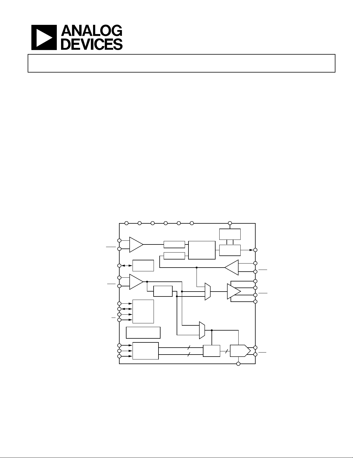
FUNCTIONAL BLOCK DIAGRAM
AVDD AGND DVDD DGND VCML VCP CP_RSET
REFIN
REFIN
SYNC, PLL
LOCK
CLK1
CLK1
SCLK
SDI/O
SDO
CS
SERIAL
CONTROL
PORT
TIMING AND
CONTROL LOGIC
DIVIDER
1, 2, 4, 8
M DIVIDER
N DIVIDER
APPLICATIONS
Clocking high performance data converters
Base station clocking applications
Network (SONET/SDH) clocking
Gigabit Ethernet (GbE) clocking
Instrumentation clocking circuits
CP
REF, AMP
FREQUENCY
DETECTOR
CLK
DIVCLK
PHASE
CHARGE
PUMP
CML
CP
CLK2
CLK2
DRV_RSE
OUT0
OUT0
VCML
AD9540
S2
S1
S0
FREQUENCY
PROFILES
Rev. 0
Information furnished by Analog Devices is believed to be accurate and reliable.
However, no responsibility is assumed by Analog Devices for its use, nor for any
infringements of patents or other rights of third parties that may result from its use.
Specifications subject to change without notice. No license is granted by implication
or otherwise under any patent or patent rights of Analog Devices. Trademarks and
registered trademarks are the property of their respective owners.
PHASE/
48
14
Figure 1.
10
DDS
One Technology Way, P.O. Box 9106, Norwood, MA 02062-9106, U.S.A.
Tel: 781.329.4700
Fax: 781.326.8703 © 2004 Analog Devices, Inc. All rights reserved.
DAC
DAC_RSET
www.analog.com
IOUT
IOUT
04947-001

AD9540
TABLE OF CONTENTS
Product Overview............................................................................. 3
DDS and DAC ............................................................................ 20
Specifications..................................................................................... 4
Loop Measurement Conditions.................................................. 9
Absolute Maximum Ratings.......................................................... 10
ESD Caution................................................................................ 10
Pin Configuration and Function Descriptions........................... 11
Typical Performance Characteristics ...........................................13
Typical Application Circuits.......................................................... 18
Application Circuit Descriptions ............................................. 18
General Description ....................................................................... 19
PLL Circuitry .............................................................................. 19
CML Driver................................................................................. 19
REVISION HISTORY
7/04—Revision 0: Initial Version
Modes of Operation ....................................................................... 21
Selectable Clock Frequencies and Selectable Edge Delay ..... 21
Synchronization Modes for Multiple Devices.............................. 21
Serial Port Operation ..................................................................... 22
Instruction Byte.......................................................................... 23
Serial Interface Port Pin Description....................................... 23
MSB/LSB Transfers .................................................................... 23
Register Map and Description...................................................... 24
Control Function Register Descriptions................................. 27
Outline Dimensions....................................................................... 32
Ordering Guide .......................................................................... 32
Rev. 0 | Page 2 of 32

AD9540
PRODUCT OVERVIEW
The AD9540 is Analog Devices’ first dedicated clocking product
specifically designed to support the extremely stringent clocking requirements of the highest performance data converters.
The device features high performance PLL circuitry, including a
flexible 200 MHz phase frequency detector and a digitally
controlled charge pump current. The device also provides a low
jitter, 655 MHz CML-mode, PECL-compliant output driver with
programmable slew rates. External VCO rates up to 2.7 GHz are
supported. Extremely fine tuning resolution (steps less than
2.33 µHz) is another feature supported by this device. Information is loaded into the AD9540 via a serial I/O port that has a
device write-speed of 25 Mb/s. The AD9540 frequency
divider block can also be programmed to support a spread
spectrum mode of operation.
The AD9540 is specified to operate over the extended
automotive range of −40°C to +85°C.
Rev. 0 | Page 3 of 32

AD9540
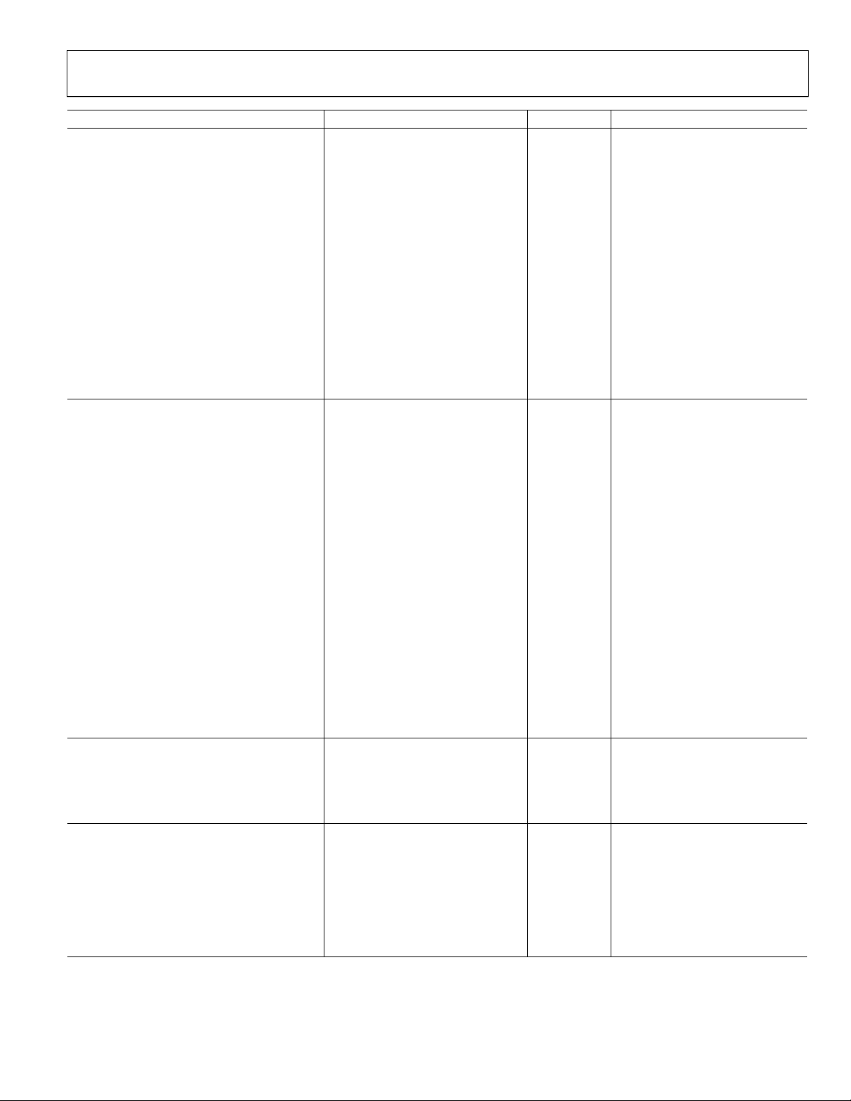
SPECIFICATIONS
AVDD = DVDD = 1.8 V ± 5%; DVDD_I/O = CP_VDD = 3.3 V ± 5% (@ TA = 25°C), DAC_R
DRV_R
= 4.02 kΩ, unless otherwise noted.
SET
Table 1.
Parameter Min Typ Max Unit Test Conditions/Comments
TOTAL SYSTEM JITTER AND PHASE NOISE FOR
105 MHz ADC CLOCK GENERATION CIRCUIT
Converter Limiting Jitter1 720 fS rms
Resultant SNR 59.07 dB
Phase Noise of Fundamental
@ 10 Hz Offset 80 dBc/Hz
@ 100 Hz Offset 92 dBc/Hz
@ 1 kHz Offset 101 dBc/Hz
@ 10 kHz Offset 110 dBc/Hz
@ 100 kHz Offset 147 dBc/Hz
≥1 MHz Offset 153 dBc/Hz
TOTAL SYSTEM PHASE NOISE FOR 210 MHz
ADC CLOCK GENERATION CIRCUIT
Phase Noise of Fundamental
@ 10 Hz Offset 79.2 dBc/Hz
@ 100 Hz Offset 86 dBc/Hz
@ 1 kHz Offset 95 dBc/Hz
@ 10 kHz Offset 105 dBc/Hz
@ 100 kHz Offset 144 dBc/Hz
@ 1 MHz Offset 151 dBc/Hz
TOTAL SYSTEM TIME JITTER FOR CLOCKS
155.52 MHz Clock 581 fS rms 12 kHz to 1.3 MHz bandwidth
622.08 MHz Clock 188 fS rms 12 kHz to 5 MHz bandwidth
RF DIVIDER/CML DRIVER EQUIVALENT
INTRINSIC TIME JITTER
FIN = 414.72 MHz, F
FIN = 1244.16 MHz, F
FIN = 2488.32 MHz, F
= 51.84 MHz 136 fS rms R = 8, BW = 12 kHz to 400 kHz
OUT
= 155.52 MHz 101 fS rms R = 8, BW = 12 kHz to 1.3 MHz
OUT
= 622.08 MHz 108 fS rms R = 4, BW = 12 kHz to 5 MHz
OUT
RF DIVIDER/CML DRIVER RESIDUAL PHASE NOISE
FIN = 81.92 MHz, F
= 10.24 MHz RF Divider R = 8
OUT
@ 10 Hz 120 dBc/Hz
@ 100 Hz 128 dBc/Hz
@ 1 kHz 137 dBc/Hz
@ 10 kHz 145 dBc/Hz
@ 100 kHz 150 dBc/Hz
≥1 MHz 153 dBc/Hz
FIN = 983.04 MHz, F
= 122.88 MHz RF Divider R = 8
OUT
@ 10 Hz 115 dBc/Hz
@ 100 Hz 125 dBc/Hz
@ 1 KHz 132 dBc/Hz
@ 10 kHz 142 dBc/Hz
@ 100 kHz 146 dBc/Hz
@ 1 MHz 151 dBc/Hz
>3 MHz 153 dBc/Hz
= 3.92 kΩ, CP_R
SET
= 3.09 kΩ,
SET
Rev. 0 | Page 4 of 32

AD9540
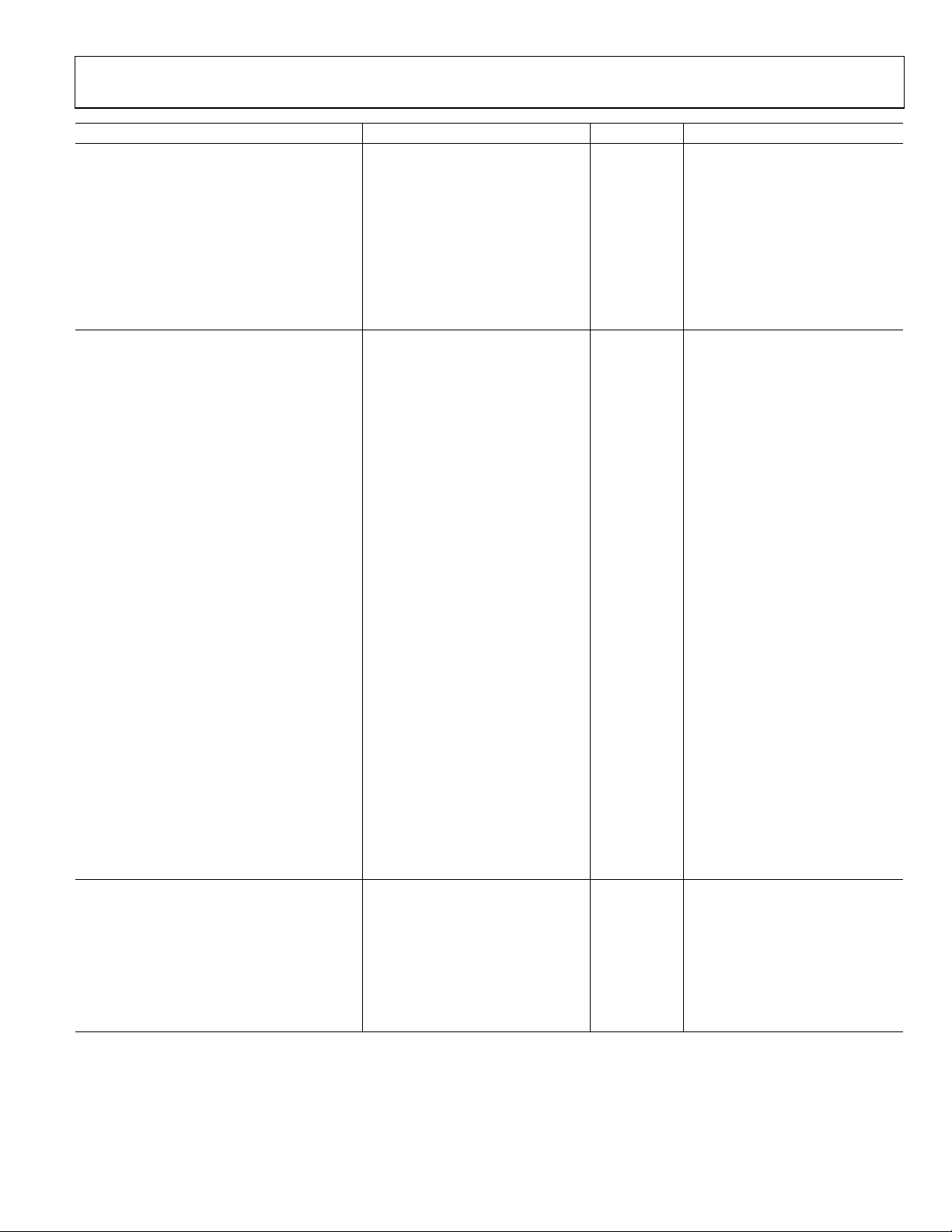
Parameter Min Typ Max Unit Test Conditions/Comments
FIN = 1966.08 MHz, F
@ 10 Hz 105 dBc/Hz
@ 100 Hz 112 dBc/Hz
@ 1 kHz 122 dBc/Hz
@ 10 kHz 130 dBc/Hz
@ 100 kHz 141 dBc/Hz
@ 1 MHz 144 dBc/Hz
>3 MHz 146 dBc/Hz
FIN = 2488 MHz, F
@ 10 Hz 100 dBc/Hz
@ 100 Hz 108 dBc/Hz
@ 1 kHz 115 dBc/Hz
@ 10 kHz 125 dBc/Hz
@ 100 kHz 135 dBc/Hz
@ 1 MHz 140 dBc/Hz
≥3 MHz 142 dBc/Hz
PHASE FREQUENCY DETECTOR/CHARGE PUMP
REFIN Input
Input Frequency2
÷M Set to Divide by at Least 4 655 MHz
÷M Bypassed 200 MHz
Input Voltage Levels 200 450 600 mV p-p
Input Capacitance 10 pF
Input Resistance 1500 Ω
CLK2 Input
Input Frequency
÷N Set to Divide by at Least 4 655 MHz
÷N Bypassed 200 MHz
Input Voltage Levels 200 450 600 mV p-p
Input Capacitance 10 pF
Input Resistance 1500 Ω
Charge Pump Source/Sink Maximum Current 4 mA
Charge Pump Source/Sink Accuracy 5 %
Charge Pump Source/Sink Matching 2 %
Charge Pump Output Compliance Range3 0.5 CPVDD − 0.5 V
STATUS Drive Strength 2 mA
PHASE FREQUENCY DETECTOR NOISE FLOOR
@ 50 kHz PFD Frequency 148 dBc/Hz
@ 2 MHz PFD Frequency 133 dBc/Hz
@ 100 MHz PFD Frequency 116 dBc/Hz
@ 200 MHz PFD Frequency 113 dBc/Hz
RF DIVIDER (CLK1 ) INPUT SECTION (÷R)
RF Divider Input Range 1 2700 MHz
Input Capacitance (DC) 3 pF
Input Impedance (DC) 1500 Ω
Input Duty Cycle 42 50 58 %
Input Power/Sensitivity −10 +4 dBm Single-ended, into a 50 Ω load4
Input Voltage Level 200 1000 mV p-p
= 491.52 MHz RF Divider R = 4
OUT
= 622 MHz RF Divider R = 4
OUT
DDS SYSCLK not to
exceed 400 MSPS
Rev. 0 | Page 5 of 32

AD9540
Parameter Min Typ Max Unit Test Conditions/Comments
CML OUTPUT DRIVER (OUT0)
Differential Output Voltage Swing5 720 mV 50 Ω load to supply, both lines
Maximum Toggle Rate 655
Common-Mode Output Voltage 1.75 V
Output Duty Cycle 42 58 %
Output Current
Continuous6 7.2 mA
Rising Edge Surge 20.9 mA
Falling Edge Surge 13.5 mA
Output Rise Time 250 ps 100 Ω terminated, 5 pF load
Output Fall Time 250 ps 100 Ω terminated, 5 pF load
LOGIC INPUTS (SDI/O, I/O_RESET, RESET,
I/O_UPDATE, S0, S1, S2, SYNC_IN)
7
VIH, Input High Voltage 2.0 V
VIL, Input Low Voltage 0.8 V
I
, I
, Input Current ±1 ±5 µA
INH
INL
CIN, Maximum Input Capacitance 3 pF
LOGIC OUTPUTS (SDO, SYNC_OUT, STATUS)8
VOH, Output High Voltage 2.7 V
VOH, Output Low Voltage 0.4 V
IOH 100 µA
IOL 100 µA
POWER CONSUMPTION
Total Power Consumed, All Functions On 400 mW
IAVDD 85 mA
IDVDD 45 mA
IDVDD_I/O 20 mA
ICPVDD 15 mA
Power-Down Mode 80 mW
WAKE-UP TIME (FROM POWER-DOWN MODE)
Digital Power-Down (CFR1<7>) 12 ns
DAC Power-Down (CFR2<39>) 7 µs
RF Divider Power-Down (CFR2<23>) 400 ns
Clock Driver Power-Down (CFR2<20>) 6 µs
Charge Pump Full Power-Down (CFR2<4>) 10 µs
Charge Pump Quick Power-Down (CFR2<3>) 150 ns
CRYSTAL OSCILLATOR (ON REFIN INPUT)
Operating Range 20 25 30 MHz
Residual Phase Noise (@ 25 MHz)
@ 10 Hz Offset 95 dBc/Hz
@ 100 Hz Offset 120 dBc/Hz
@ 1 kHz Offset 140 dBc/Hz
@ 10 kHz Offset 157 dBc/Hz
@ 100 kHz Offset 164 dBc/Hz
>1 MHz Offset 168 dBc/Hz
DIGITAL TIMING SPECIFICATIONS
CS
to SCLK Setup Time TPRE
Period of SCLK (Write) TSCLKW 40 ns
Period of SCLK (Read) TSCLKR 400 ns
Serial Data Setup Time TDSU 6.5 ns
Serial Data Hold Time TDHD 0 ns
Data Valid Time TDV 40 ns
6 ns
Rev. 0 | Page 6 of 32

AD9540
Parameter Min Typ Max Unit Test Conditions/Comments
I/O Update to SYNC_CLK Setup Time 7 ns
PS<2:0> to SYNC_CLK Setup Time 7 ns
Latencies/Pipeline Delays
I/O Update to DAC Frequency Change 33 SYSCLK Cycles
I/O Update to DAC Phase Change 33 SYSCLK Cycles
PS<2:0> to DAC Frequency Change 29 SYSCLK Cycles
PS<2:0> to DAC Phase Change 29 SYSCLK Cycles
I/O Update to CP_OUT Scaler Change 4 SYSCLK Cycles
I/O Update to Frequency Accumulator
Step Size Change
DAC OUTPUT CHARACTERISTICS
Resolution 10 Bits
Full-Scale Output Current 10 15 mA
Gain Error −10 +10 % FS
Output Offset 0.6 µA
Output Capacitance 5 pF
Voltage Compliance Range AVDD − 0.50 AVDD + 0.50
Wideband SFDR (DC to Nyquist)
10 MHz Analog Out 65 dBc
40 MHz Analog Out 62 dBc
80 MHz Analog Out 57 dBc
120 MHz Analog Out 56 dBc
160 MHz Analog Out 54 dBc
Narrow-Band SFDR
10 MHz Analog Out (±1 MHz) 83 dBc
10 MHz Analog Out (±250 kHz) 85 dBc
10 MHz Analog Out (±50 kHz) 86 dBc
40 MHz Analog Out (±1 MHz) 82 dBc
40 MHz Analog Out (±250 kHz) 84 dBc
40 MHz Analog Out (±50 kHz) 87 dBc
80 MHz Analog Out (±1 MHz) 80 dBc
80 MHz Analog Out (±250 kHz) 82 dBc
80 MHz Analog Out (±50 kHz) 86 dBc
120 MHz Analog Out (±1 MHz) 80 dBc
120 MHz Analog Out (±250 kHz) 82 dBc
120 MHz Analog Out (±50 kHz) 84 dBc
160 MHz Analog Out (±1 MHz) 80 dBc
160 MHz Analog Out (±250 kHz) 82 dBc
160 MHz Analog Out (±50 kHz) 84 dBc
DAC RESIDUAL PHASE NOISE
19.7 MHz F
@ 10 Hz Offset 122 dBc/Hz
@ 100 Hz Offset 134 dBc/Hz
@ 1 kHz Offset 143 dBc/Hz
@ 10 kHz Offset 150 dBc/Hz
@ 100 kHz Offset 158 dBc/Hz
>1 MHz Offset 160 dBc/Hz
OUT
4 SYSCLK Cycles
Rev. 0 | Page 7 of 32

AD9540
Parameter Min Typ Max Unit Test Conditions/Comments
51.84 MHz F
@ 10 Hz Offset 110 dBc/Hz
@ 100 Hz Offset 121 dBc/Hz
@ 1 kHz Offset 135 dBc/Hz
@ 10 kHz Offset 142 dBc/Hz
@ 100 kHz Offset 148 dBc/Hz
> 1 MHz Offset 153 dBc/Hz
105 MHz Analog Out
@ 10 Hz Offset 105 dBc/Hz
@ 100 Hz Offset 115 dBc/Hz
@ 1 kHz Offset 126 dBc/Hz
@ 10 kHz Offset 132 dBc/Hz
@ 100 kHz Offset 140 dBc/Hz
>1 MHz Offset 145 dBc/Hz
155.52 MHz Analog Out
@ 10 Hz Offset 100 dBc/Hz
@ 100 Hz Offset 112 dBc/Hz
@ 1 kHz Offset 123 dBc/Hz
@ 10 kHz Offset 131 dBc/Hz
@ 100 kHz Offset 138 dBc/Hz
>1 MHz Offset 144 dBc/Hz
OUT
1
The SNR of a 14-bit ADC was measured with an ENCODE rate of 105 MSPS and an AIN of 170 MHz. The resultant SNR was known to be limited by the jitter of the clock,
not by the noise on the AIN signal. From this SNR value, the jitter affecting the measurement can be back calculated.
2
Driving the PLLREF input buffer. The crystal oscillator section of this input stage performs up to only 30 MHz.
3
The charge pump output compliance range is functionally 0.2 V to (CPVDD − 0.2 V). The value listed here is the compliance range for 5% matching.
4
The input impedance of the CLK1 input is 1500 Ω. However, to provide matching on the clock line, an external 50 Ω load is used.
5
Measured as peak-to-peak between DAC outputs.
6
For a 4.02 kΩ resistor from DRV_RSET to GND.
7
IBIS models for the digital I/O pins available upon request.
8
Assumes a 1 mA load.
Rev. 0 | Page 8 of 32

AD9540
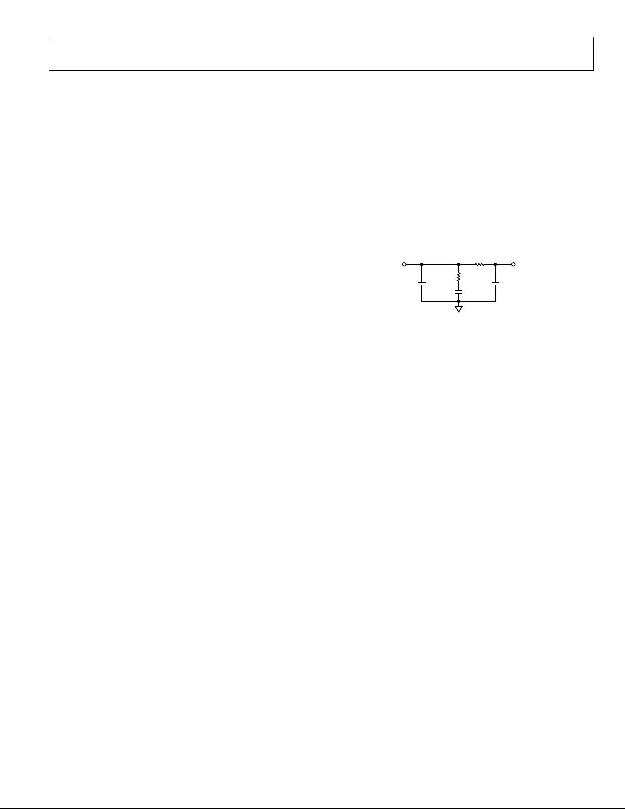
LOOP MEASUREMENT CONDITIONS
622 MHz OC-12 Clock
VCO = Sirenza 190-640T
105 MHz Converter Clock
VCO = Sirenza 190-845T
Reference = Wenzel 500-10116 (30.3 MHz)
Loop Filter = 10 kHz BW, 60° Phase Margin
C1 = 170 nF, R1 = 14.4 Ω, C2 = 5.11 µF, R2 = 89.3 Ω,
C3 Omitted
CP_OUT = 4 mA (Scaler = ×8)
÷R = 2, ÷M = 1, ÷N = 1
Reference = Wenzel 500-10116 (30.3 MHz)
Loop Filter = 10 kHz BW, 45° Phase Margin
C1 = 117 nF, R1 = 28 Ω, C2 = 1.6 µF, R2 = 57.1 Ω, C3 = 53.4 nF
CP_OUT = 4 mA (Scaler = ×8)
÷R = 8, ÷M = 1, ÷N = 1
INPUT OUTPUT
C1
Figure 2. Generic Loop Filter
R2
R1
C2
C3
04806-0-033
Rev. 0 | Page 9 of 32

AD9540
ABSOLUTE MAXIMUM RATINGS
Table 2.
Parameter Rating
Analog Supply Voltage (AVDD) 2 V
Digital Supply Voltage (DVDD) 2 V
Digital I/O Supply Voltage
(DVDD_I/0)
Charge Pump Supply Voltage
(CPVDD)
Maximum Digital Input Voltage −0.5 V to DVDD_I/O + 0.5 V
Storage Temperature −65°C to +150°C
Operating Temperature Range −40°C to +125°C
Lead Temperature Range
(Soldering 10 sec)
Junction Temperature 150°C
Thermal Resistance (θJA) 26°C/W
Stresses above those listed under Absolute Maximum Ratings
may cause permanent damage to the device. This is a stress
rating only; functional operation of the device at these or any
other condition s above those indicated in the operational
section of this specification is not implied. Exposure to absolute
maximum rating conditions for extended periods may affect
device reliability.
3.6 V
3.6 V
300°C
ESD CAUTION
ESD (electrostatic discharge) sensitive device. Electrostatic charges as high as 4000 V readily accumulate on the
human body and test equipment and can discharge without detection. Although this product features proprietary ESD protection circuitry, permanent damage may occur on devices subjected to high energy electrostatic
discharges. Therefore, proper ESD precautions are recommended to avoid performance degradation or loss of
functionality.
Rev. 0 | Page 10 of 32
 Loading...