

Low Jitter Clock Generator with
6 LVPECL/LVDS/HSTL/13 LVCMOS Outputs
FEATURES
Output frequency: <1 MHz to 1 GHz
Start-up frequency accuracy: <±100 ppm (determined by
VCXO reference accuracy)
Zero delay operation
Input-to-output edge timing: <±150 ps
6 outputs: configurable LVPECL, LVDS, HSTL, and LVCMOS
6 dedicated output dividers with jitter-free adjustable delay
Adjustable delay: 63 resolution steps of ½ period of VCO
output divider
Output-to-output skew: <±50 ps
Duty-cycle correction for odd divider settings
Automatic synchronization of all outputs on power-up
Absolute output jitter: <200 fs at 122.88 MHz
Integration range: 12 kHz to 20 MHz
Distribution phase noise floor: −160 dBc/Hz
Digital lock detect
Nonvolatile EEPROM stores configuration settings
SPI- and I²C-compatible serial control port
Dual PLL architecture
PLL1
Low bandwidth for reference input clock cleanup with
external VCXO
Phase detector rate of 300 kHz to 75 MHz
Redundant reference inputs
Auto and manual reference switchover modes
Revertive and nonrevertive switching
Loss of reference detection with holdover mode
Low noise LVCMOS output from VCXO used for RF/IF
synthesizers
PLL2
Phase detector rate of up to 250 MHz
Integrated low noise VCO
APPLICATIONS
LTE and multicarrier GSM base stations
Wireless and broadband infrastructure
Medical instrumentation
Clocking high speed ADCs, DACs, DDSs, DDCs, DUCs, MxFEs
Low jitter, low phase noise clock distribution
Clock generation and translation for SONET, 10Ge, 10G FC,
and other 10 Gbps protocols
Forward error correction (G.710)
High performance wireless transceivers
ATE and high performance instrumentation
AD9524
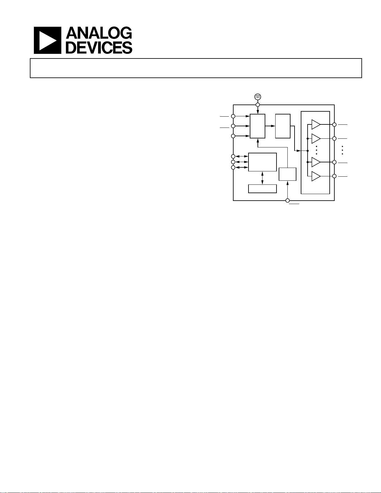
FUNCTIONAL BLOCK DIAGRAM
OSC
REFA,
REFA
REFB,
REFB
REF_TEST
SCLK/SCL
SDIO/SDA
SDO
PLL1
CONTROL
INTERFACE
(SPI AND I
EEPROM
PLL2
2
C)
ZD_IN, ZD_IN
Figure 1.
ZERO
DELAY
GENERAL DESCRIPTION
The AD9524 provides a low power, multi-output, clock
distribution function with low jitter performance, along with an
on-chip PLL and VCO. The on-chip VCO tunes from 3.6 GHz to
4.0 GHz.
The AD9524 is defined to support the clock requirements for
long term evolution (LTE) and multicarrier GSM base station
designs. It relies on an external VCXO to provide the reference
jitter cleanup to achieve the restrictive low phase noise requirements necessary for acceptable data converter SNR performance.
The input receivers, oscillator, and zero delay receiver provide
both single-ended and differential operation. When connected
to a recovered system reference clock and a VCXO, the device
generates six low noise outputs with a range of 1 MHz to 1 GHz
and one dedicated buffered output from the input PLL (PLL1).
The frequency and phase of one clock output relative to another
clock output can be varied by means of a divider phase select
function that serves as a jitter-free coarse timing adjustment in
increments that are equal to one-half the period of the signal
coming out of the VCO.
An in-package EEPROM can be programmed through the serial
interface to store user-defined register settings for power-up
and chip reset.
AD9524
6-CLOCK
DISTRIBUTI ON
OUT0,
OUT0
OUT1,
OUT1
OUT4,
OUT4
OUT5,
OUT5
09081-001
Rev. C
Information furnished by Analog Devices is believed to be accurate and reliable. However, no
responsibility is assumed by Anal og Devices for its use, nor for any infringements of patents or ot her
rights of third parties that may result from its use. Specifications subject to change without notice. No
license is granted by implication or otherwise under any patent or patent rights of Analog Devices.
Trademarks and registered trademarks are the property of their respective owners.
One Technology Way, P.O. Box 9106, Norwood, MA 02062-9106, U.S.A.
Tel: 781.329.4700 www.analog.com
Fax: 781.461.3113 ©2010–2011 Analog Devices, Inc. All rights reserved.

AD9524
TABLE OF CONTENTS
Features.............................................................................................. 1
Applications....................................................................................... 1
Functional Block Diagram .............................................................. 1
General Description ......................................................................... 1
Revision History ............................................................................... 3
Specifications..................................................................................... 4
Conditions..................................................................................... 4
Supply Current.............................................................................. 4
Power Dissipation......................................................................... 6
REFA
REFA,
ZD_IN
OSC_CTRL Output Characteristics .......................................... 7
REF_TEST Input Characteristics............................................... 7
PLL1 Output Characteristics ...................................................... 7
Distribution Output Characteristics (OUT0,
OUT5
Timing Alignment Characteristics............................................. 9
Jitter and Noise Characteristics .................................................. 9
PLL2 Characteristics .................................................................... 9
Logic Input Pins—PD,
REF_SEL...................................................................................... 10
Status Output Pins—STATUS1, STATUS0 ............................. 10
Serial Control Port—SPI Mode................................................ 10
Serial Control Port—IC Mode................................................ 11
Absolute Maximum Ratings.......................................................... 12
Thermal Resistance .................................................................... 12
ESD Caution................................................................................ 12
Pin Configuration and Function Descriptions........................... 13
Typical Performance Characteristics ........................................... 15
, REFB,
Input Characteristics...................................................... 6
)............................................................................................ 8
REFB
, OSC_IN,
SYNC, RESET
OSC_IN
, EEPROM_SEL,
, and ZD_IN,
OUT0
to OUT5,
Input/Output Termination Recommendations.......................... 17
Terminology.................................................................................... 18
Theory of Operation ...................................................................... 19
Detailed Block Diagram ............................................................ 19
Overview ..................................................................................... 19
Component Blocks—Input PLL (PLL1).................................. 20
Component Blocks—Output PLL (PLL2) .............................. 21
Clock Distribution ..................................................................... 23
Zero Delay Operation................................................................ 25
Serial Control Port ......................................................................... 26
SPI/IC Port Selection................................................................ 26
IC Serial Port Operation.......................................................... 26
SPI Serial Port Operation.......................................................... 29
SPI Instruction Word (16 Bits)................................................. 30
SPI MSB/LSB First Transfers .................................................... 30
EEPROM Operations..................................................................... 33
Writing to the EEPROM ........................................................... 33
Reading from the EEPROM ..................................................... 33
Programming the EEPROM Buffer Segment......................... 34
Power Dissipation and Thermal Considerations....................... 36
Clock Speed and Driver Mode ................................................. 36
Evaluation of Operating Conditions........................................ 36
Thermally Enhanced Package Mounting Guidelines............ 36
Control Registers............................................................................ 37
Control Register Map ................................................................ 37
Control Register Map Bit Descriptions................................... 41
Outline Dimensions....................................................................... 53
Ordering Guide .......................................................................... 53
Rev. C | Page 2 of 56

AD9524
REVISION HISTORY
6/11—Rev. B to Rev. C
Changes to Table 2, Clock Output Drivers—Lower Power Mode
Off and Clock Output Drivers—Lower Power Mode On
Parameters..........................................................................................4
Changes to Table 3, Incremental Power Dissipation, Low Power
Typical Configuration Parameters..................................................6
Changes to Table 17 ........................................................................12
Changes to Overview Section, Crystal Oscillator Values ..........19
Changes to Power Dissipation and Thermal Considerations
Section ..............................................................................................36
Deleted Examples from Evaluation of Operating Conditions
Section ..............................................................................................37
Changes to Table 30, Register 0x1BB Bit Values.........................40
Changes to Table 52 Bit Values......................................................49
3/11—Rev. A to Rev. B
Added Table Summary, Table 8.......................................................7
Changes to Table 9 ............................................................................8
Changes to EEPROM Operations Section and Writing to the
EEPROM Section ............................................................................32
Changes to Addr (Hex) 0x01A, Bits[4:3], Table 30.....................37
Changes to Bits[4:3], Table 40 .......................................................43
1/11—Rev. 0 to Rev. A
Changes to General Description Section .......................................1
Changes to Specifications Summary Statement............................4
Changes to Test Conditions/Comments for VDD3_PLL1,
Supply Voltage for PLL1 Parameter, Table 2..................................4
Changes to Typical Configuration and Low Power Typical
Configuration Parameters, Table 3 .................................................5
Changes to Input High Voltage and Input Low Voltage
Parameters; Added Input Threshold Voltage Parameter,
Table 4 ................................................................................................. 5
Changed Differential Output Voltage Swing Parameters to
Differential Output Voltage Magnitude; Changes to Test
Conditions/Comments, Table 8 ......................................................7
Changed Junction Temperature Parameter from 150°C to
115°C, Table 16 ................................................................................11
Added Figure 14; Renumbered Sequentially...............................15
Changes to Figure 15, Figure 17, and Figure 19; Change to
Caption of Figure 21.......................................................................16
Added PLL1 Lock Detect Section .................................................19
Changes to VCO Calibration Section...........................................21
Changed Output Mode Section to Multimode Output
Drivers; Changes to Multimode Output Drivers Section..........22
Changes to Figure 29......................................................................24
Changes to SPI/I2C Port Selection Section .................................25
Change to SPI Instruction Word (16 Bits) Section.....................29
Added Power Dissipation and Thermal Considerations
Section ..............................................................................................35
Changes to Table 34 to Table 36 and Table 38.............................42
Change to Register 0x0F3, Bit 1 Description, Table 47.............. 45
Change to Register 0x198, Bits[7:2], Table 50 ............................. 47
Changes to Table 52 ........................................................................48
Changes to Register 0x230 and Register 0x231, Table 54..........49
7/10—Revision 0: Initial Version
Rev. C | Page 3 of 56
AD9524
SPECIFICATIONS
f
= 122.88 MHz single-ended, REFA and REFB on differential at 30.72 MHz, f
VCXO
power mode off, divider phase =1, unless otherwise noted. Typical is given for VDD = 3.3 V ± 5%, and T
noted. Minimum and maximum values are given over the full VDD and T
(−40°C to +85°C) variation, as listed in Tab l e 1 .
A
CONDITIONS
Table 1.
Parameter Min Typ Max Unit Test Conditions/Comments
SUPPLY VOLTAGE
VDD3_PLL1, Supply Voltage for PLL1 3.3 V 3.3 V ± 5%
VDD3_PLL2, Supply Voltage for PLL2 3.3 V 3.3 V ± 5%
VDD3_REF, Supply Voltage Clock Output Drivers Reference 3.3 V 3.3 V ± 5%
VDD1.8_PLL2, Supply Voltage for PLL2 1.8 V 1.8 V ± 5%
VDD3_OUT[x:y],1 Supply Voltage Clock Output Drivers 3.3 V 3.3 V ± 5%
VDD1.8_OUT[x:y],1 Supply Voltage Clock Dividers 1.8 V 1.8 V ± 5%
TEMPERATURE RANGE, TA −40 +25 +85 °C
1
x and y are the pair of differential outputs that share the same power supply. For example, VDD3_OUT[0:1] is Supply Voltage Clock Output OUT0,
respectively) and Supply Voltage Clock Output OUT1,
OUT1
(Pin 38 and Pin 37, respectively).
SUPPLY CURRENT
Table 2.
Parameter Min Typ Max Unit Test Conditions/Comments
SUPPLIES OTHER THAN CLOCK OUTPUT DRIVERS
VDD3_PLL1, Supply Voltage for PLL1 22 25.2 mA Decreases by 9 mA typical if REFB is turned off
VDD3_PLL2, Supply Voltage for PLL2 67 77.7 mA
VDD3_REF, Supply Voltage Clock Output Drivers Reference
LVPECL Mode 5 6 mA
LVDS Mode 4 4.8 mA
HSTL Mode 3 3.6 mA
CMOS Mode 3 3.6 mA
VDD1.8_PLL2, Supply Voltage for PLL2 15 18 mA
VDD1.8_OUT[x:y],1 Supply Voltage Clock Dividers2 3.5 4.2 mA Current for each divider: f = 245.76 MHz
CLOCK OUTPUT DRIVERS—LOWER POWER MODE OFF Channel x control register, Bit 4 = 0
LVDS Mode, 7 mA
VDD3_OUT[x:y],1 Supply Voltage Clock Output Drivers 11.5 13.2 mA f = 122.88 MHz
VDD3_OUT[x:y],1 Supply Voltage Clock Output Drivers 40 45 mA f = 983.04 MHz
LVDS Mode, 3.5 mA
VDD3_OUT[x:y],1 Supply Voltage Clock Output Drivers 6.5 7.5 mA f = 122.88 MHz
VDD3_OUT[x:y],1 Supply Voltage Clock Output Drivers 23 26.3 mA f = 983.04 MHz
LVPECL Mode
VDD3_OUT[x:y],1 Supply Voltage Clock Output Drivers 13 14.4 mA f = 122.88 MHz
VDD3_OUT[x:y],1 Supply Voltage Clock Output Drivers 41 46.5 mA f = 983.04 MHz
HSTL Mode, 8 mA
VDD3_OUT[x:y],1 Supply Voltage Clock Output Drivers 14 16.3 mA f = 122.88 MHz
CMOS Mode (Single-Ended)
VDD3_OUT[x:y],1 Supply Voltage Clock Output Drivers 2 2.4 mA f = 15.36 MHz, 10 pF load
= 3932.16 MHz, doubler is off, channel control low
VCO
= 25°C, unless otherwise
A
OUT0
(Pin 41 and Pin 40,
Only one output driver turned on; for each
additional output that is turned on, the current
increments by 1.2 mA maximum
Only one output driver turned on; for each
additional output that is turned on, the current
increments by 1.2 mA maximum
Values are independent of the number of
outputs turned on
Values are independent of the number of
outputs turned on
Rev. C | Page 4 of 56
AD9524
Parameter Min Typ Max Unit Test Conditions/Comments
CLOCK OUTPUT DRIVERS—LOWER POWER MODE ON Channel x control register, Bit 4 = 1
LVDS Mode, 7 mA
VDD3_OUT[x:y],1 Supply Voltage Clock Output Drivers 10 10.8 mA f = 122.88 MHz
VDD3_OUT[x:y],1 Supply Voltage Clock Output Drivers 27 29.8 mA f = 983.04 MHz
LVDS Mode, 3.5 mA
VDD3_OUT[x:y],1 Supply Voltage Clock Output Drivers 6.5 7.5 mA f = 122.88 MHz
VDD3_OUT[x:y],1 Supply Voltage Clock Output Drivers 23 26.3 mA f = 983.04 MHz
LVPECL Mode
VDD3_OUT[x:y],1 Supply Voltage Clock Output Drivers 11 12.4 mA f = 122.88 MHz
VDD3_OUT[x:y],1 Supply Voltage Clock Output Drivers 28 31.2 mA f = 983.04 MHz
HSTL Mode, 16 mA
VDD3_OUT[x:y],1 Supply Voltage Clock Output Drivers 20 24.3 mA f = 122.88 MHz
VDD3_OUT[x:y],1 Supply Voltage Clock Output Drivers 50 59.1 mA f = 983.04 MHz
HSTL Mode, 8 mA
VDD3_OUT[x:y],1 Supply Voltage Clock Output Drivers 11 12.7 mA f = 122.88 MHz
VDD3_OUT[x:y],1 Supply Voltage Clock Output Drivers 27 31.8 mA f = 983.04 MHz
1
x and y are the pair of differential outputs that share the same power supply. For example, VDD3_OUT[0:1] is Supply Voltage Clock Output OUT0,
respectively) and Supply Voltage Clock Output OUT1,
2
The current for Pin 34 (VDD1.8_OUT[0:3]) is 2× that of the other VDD1.8_OUT[x:y] pairs.
OUT1
(Pin 38 and Pin 37, respectively).
OUT0
(Pin 41 and Pin 40,
Rev. C | Page 5 of 56

AD9524
POWER DISSIPATION
Table 3.
Parameter Min Typ Max Unit Test Conditions/Comments
POWER DISSIPATION Does not include power dissipated in termination resistors
Typical Configuration 571 680 mW
PD, Power-Down
101 132.2 mW
INCREMENTAL POWER DISSIPATION
Low Power Typical Configuration 367 428.4 mW
Switched to One Input,
−28.5 −8 mW Running at 30.72 MHz
Reference Single-Ended Mode
Switched to Two Inputs,
26 44.6 mW Running at 30.72 MHz
Reference Differential Mode
Switched to Two Inputs,
−27.5 −5.1 mW Running at 30.72 MHz
Reference Single-Ended Mode
Output Distribution, Driver On Incremental power increase (OUT1) from low power typical (3.3 V)
LVDS 15.3 18.4 mW Single 3.5 mA LVDS output at 245.76 MHz
47.8 55.4 mW Single 7 mA LVDS output at 61.44 MHz
LVPECL 50.1 54.9 mW Single LVPECL output at 122.88 MHz
HSTL 40.2 46.3 mW Single 8 mA HSTL output at 122.88 MHz
43.7 50.3 mW Single 16 mA HSTL output at 122.88 MHz
CMOS 6.6 7.9 mW Single 3.3 V CMOS output at 15.36 MHz
9.9 11.9 mW Dual complementary 3.3 V CMOS output at 15.36 MHz
9.9 11.9 mW Dual in-phase 3.3 V CMOS output at 15.36 MHz
REFA, REFA, REFB, REFB, OSC_IN, OSC_IN, AND ZD_IN, ZD_IN INPUT CHARACTERISTICS
Clock distribution outputs running as follows: four LVPECL outputs
at 122.88 MHz, two LVDS outputs (3.5 mA) at 122.88 MHz,
one differential input reference at 30.72 MHz; f
f
= 3932.16 MHz; PLL2 BW = 530 kHz; doubler is off
VCO
= 122.88 MHz,
VCXO
PD pin pulled low, with typical configuration conditions
Absolute total power with clock distribution; one LVPECL output
running at 122.88 MHz; one differential input reference at
30.72 MHz; f
= 122.88 MHz, f
VCXO
= 3932.16 MHz; doubler is off
VCO
Table 4.
Parameter Min Typ Max Unit Test Conditions/Comments
DIFFERENTIAL MODE
Input Frequency Range 400 MHz
Input Slew Rate (OSC_IN) 400 V/µs Minimum limit imposed for jitter performance
Common-Mode Internally
0.6 0.7 0.8 V
Generated Input Voltage
Input Common-Mode Range 1.025 1.475 V For dc-coupled LVDS (maximum swing)
Differential Input Voltage,
Sensitivity Frequency < 250 MHz
100 mV p-p
Capacitive coupling required; can accommodate single-ended
input by ac grounding of unused input; the instantaneous voltage
on either pin must not exceed the 1.8 V dc supply rails
Differential Input Voltage,
Sensitivity Frequency > 250 MHz
200 mV p-p
Capacitive coupling required; can accommodate single-ended
input by ac grounding of unused input; the instantaneous voltage
on either pin must not exceed the 1.8 V dc supply rails
Differential Input Resistance 4.8 kΩ
Differential Input Capacitance 1 pF
Duty Cycle Duty cycle bounds are set by pulse width high and pulse width low
Pulse Width Low 1 ns
Pulse Width High 1 ns
CMOS MODE SINGLE-ENDED INPUT
Input Frequency Range 250 MHz
Input High Voltage 1.6 V
Input Low Voltage 0.52 V
Input Threshold Voltage 1.0 V
When ac coupling to the input receiver, the user must dc bias the
input to 1 V; the single-ended CMOS input is 3.3 V compatible
Rev. C | Page 6 of 56

AD9524
Input Capacitance 1 pF
Duty Cycle Duty cycle bounds are set by pulse width high and pulse width low
Pulse Width Low 1.6 ns
Pulse Width High 1.6 ns
OSC_CTRL OUTPUT CHARACTERISTICS
Table 5.
Parameter Min Typ Max Unit Test Conditions/Comments
OUTPUT VOLTAGE
High VDD3_PLL1 − 0.15 V R
Low 150 mV
REF_TEST INPUT CHARACTERISTICS
Table 6.
Parameter Min Typ Max Unit Test Conditions/Comments
REF_TEST INPUT
Input Frequency Range 250 MHz
Input High Voltage 2.0 V
Input Low Voltage 0.8 V
LOAD
> 20 kΩ
PLL1 OUTPUT CHARACTERISTICS
Table 7.
Parameter1 Min Typ Max Unit Test Conditions/Comments
MAXIMUM OUTPUT FREQUENCY 250 MHz
Rise/Fall Time (20% to 80%) 387 665 ps 15 pF load
Duty Cycle 45 50 55 % f = 250 MHz
OUTPUT VOLTAGE HIGH Output driver static
VDD3_PLL1 − 0.25 V Load current = 10 mA
VDD3_PLL1 − 0.1 V Load current = 1 mA
OUTPUT VOLTAGE LOW Output driver static
0.2 V Load current = 10 mA
0.1 V Load current = 1 mA
1
CMOS driver strength = strong (see Table 51).
Rev. C | Page 7 of 56
AD9524
DISTRIBUTION OUTPUT CHARACTERISTICS (OUT0, OUT0 TO OUT5, OUT5)
Duty cycle performance is specified with the invert divider bit set to 1, and the divider phase bits set to 0.5. (For example, for Channel 0,
0x196[7] = 1 and 0x198[7:2] = 000001.)
Table 8.
Parameter Min Typ Max Unit Test Conditions/Comments
LVPECL MODE
Maximum Output Frequency 1 GHz Minimum VCO/maximum dividers
Rise Time/Fall Time (20% to 80%) 117 147 ps 100 Ω termination across output pair
Duty Cycle 47 50 52 % f < 500 MHz
43 48 52 % f = 500 MHz to 800 MHz
40 49 54 % f = 800 MHz to 1 GHz
Differential Output Voltage Magnitude 643 775 924 mV Voltage across pins; output driver static
Common-Mode Output Voltage VDD – 1.5 VDD − 1.4 VDD − 1.25 V Output driver static
SCALED HSTL MODE, 16 mA
Maximum Output Frequency 1 GHz Minimum VCO/maximum dividers
Rise Time/Fall Time (20% to 80%) 112 141 ps 100 Ω termination across output pair
Duty Cycle 47 50 52 % f < 500 MHz
44 48 51 % f = 500 MHz to 800 MHz
40 49 54 % f = 800 MHz to 1 GHz
Differential Output Voltage Magnitude 1.3 1.6 1.7 mV
Supply Sensitivity 0.6 mV/mV
Common-Mode Output Voltage VDD − 1.76 VDD − 1.6 VDD − 1.42 V
LVDS MODE, 3.5 mA
Maximum Output Frequency 1 GHz
Rise Time/Fall Time (20% to 80%) 138 161 ps 100 Ω termination across output pair
Duty Cycle 48 51 53 % f < 500 MHz
43 49 53 % f = 500 MHz to 800 MHz
41 49 55 % f = 800 MHz to 1 GHz
Differential Output Voltage Magnitude
Balanced 247 454 mV Voltage across pins; output driver static
Unbalanced 50 mV
Common-Mode Output Voltage 1.125 1.375 V Output driver static
Common-Mode Difference 50 mV
Short-Circuit Output Current 3.5 24 mA Output driver static
CMOS MODE
Maximum Output Frequency 250 MHz
Rise Time/Fall Time (20% to 80%) 387 665 ps 15 pF load
Duty Cycle 45 50 55 % f = 250 MHz
Output Voltage High Output driver static
VDD − 0.25 V Load current = 10 mA
VDD − 0.1 V Load current = 1 mA
Output Voltage Low Output driver static
0.2 V Load current = 10 mA
0.1 V Load current = 1 mA
Voltage across pins, output driver static;
nominal supply
Change in output swing vs. VDD3_OUT[x:y]
/∆VDD3)
(∆V
OD
Absolute difference between voltage
magnitude of normal pin and inverted pin
Voltage difference between output pins;
output driver static
Rev. C | Page 8 of 56
AD9524
TIMING ALIGNMENT CHARACTERISTICS
Table 9.
Parameter Min Typ Max Unit Test Conditions/Comments
OUTPUT TIMING SKEW
Between LVPECL, HSTL, and LVDS Outputs 38 164 ps
Between CMOS Outputs 100 300 ps Single-ended true phase high-Z mode
Adjustable Delay 0 63 Steps Resolution step; for example, 8 × 0.5/1 GHz
Resolution Step 500 ps ½ period of 1 GHz
Zero Delay
Between Input Clock Edge on REFA or
150 500 ps
REFB to ZD_IN Input Clock Edge,
External Zero Delay Mode
JITTER AND NOISE CHARACTERISTICS
Table 10.
Parameter Min Typ Max Unit Test Conditions/Comments
OUTPUT ABSOLUTE RMS TIME JITTER
LVPECL Mode, HSTL Mode, LVDS Mode
125 fs Integrated BW = 200 kHz to 5 MHz
136 fs Integrated BW = 200 kHz to 10 MHz
169 fs Integrated BW = 12 kHz to 20 MHz
212 fs Integrated BW = 10 kHz to 61 MHz
223 fs Integrated BW = 1 kHz to 61 MHz
PLL2 CHARACTERISTICS
Delay off on all outputs; maximum deviation
between rising edges of outputs; all outputs are on,
unless otherwise noted.
PLL1 settings: PFD = 7.68 MHz, I
= 63.5 µA, R
CP
= 10 kΩ,
ZERO
antibacklash pulse width is at maximum, BW = 40 Hz,
REFA and ZD_IN are set to differential mode
Application example based on a typical setup
(see Table 3); f = 122.88 MHz
Table 11.
Parameter Min Typ Max Unit Test Conditions/Comments
VCO (ON CHIP)
Frequency Range 3600 4000 MHz
Gain 45 MHz/V
PLL2 FIGURE OF MERIT (FOM) −226 dBc/Hz
MAXIMUM PFD FREQUENCY
Antibacklash Pulse Width
Minimum and Low 250 MHz
Maximum and High 125 MHz
Rev. C | Page 9 of 56
AD9524
LOGIC INPUT PINS—PD, SYNC, RESET, EEPROM_SEL, REF_SEL
Table 12.
Parameter Min Typ Max Unit Test Conditions/Comments
VOLTAGE
Input High 2.0 V
Input Low 0.8 V
INPUT LOW CURRENT ±80 ±250 µA
CAPACITANCE 3 pF
RESET TIMING
Pulse Width Low 50 ns
Inactive to Start of Register Programming 100 ns
SYNC TIMING
Pulse Width Low 1.5 ns High speed clock is CLK input signal
STATUS OUTPUT PINS—STATUS1, STATUS0
Table 13.
Parameter Min Typ Max Unit Test Conditions/Comments
VOLTAGE
Output High 2.94 V
Output Low 0.4 V
SERIAL CONTROL PORT—SPI MODE
The minus sign indicates that, due to the
internal pull-up resistor, current is flowing
out of the AD9524
Table 14.
Parameter Min Typ Max Unit Test Conditions/Comments
CS (INPUT)
Voltage
Input Logic 1 2.0 V
Input Logic 0 0.8 V
Current
Input Logic 1 30 µA
Input Logic 0 −110 µA
Input Capacitance 2 pF
SCLK (INPUT) IN SPI MODE
Voltage
Input Logic 1 2.0 V
Input Logic 0 0.8 V
Current
Input Logic 1 240 µA
Input Logic 0 1 µA
Input Capacitance 2 pF
SDIO (WHEN INPUT IS IN BIDIRECTIONAL MODE)
Voltage
Input Logic 1 2.0 V
Input Logic 0 0.8 V
Current
Input Logic 1 1 µA
Input Logic 0 1 µA
Input Capacitance 2 pF
Rev. C | Page 10 of 56
CS has an internal 40 kΩ pull-up resistor
The minus sign indicates that, due to the
internal pull-up resistor, current is flowing out
of the AD9524
SCLK has an internal 40 kΩ pull-down resistor
in SPI mode but not in I
2
C mode
AD9524
Parameter Min Typ Max Unit Test Conditions/Comments
SDIO, SDO (OUTPUTS)
Output Logic 1 Voltage 2.7 V
Output Logic 0 Voltage 0.4 V
TIMING
Clock Rate (SCLK, 1/t
Pulse Width High, t
Pulse Width Low, t
SDIO to SCLK Setup, tDS 3.3 ns
SCLK to SDIO Hold, tDH 0 ns
SCLK to Valid SDIO and SDO, tDV 14 ns
CS to SCLK Setup, tS
CS to SCLK Setup and Hold, tS, tC
CS Minimum Pulse Width High, t
SERIAL CONTROL PORT—I²C MODE
VDD = VDD3_REF, unless otherwise noted.
Table 15.
Parameter Min Typ Max Unit Test Conditions/Comments
SDA, SCL (WHEN INPUTTING DATA)
Input Logic 1 Voltage 0.7 × VDD V
Input Logic 0 Voltage 0.3 × VDD V
Input Current with an Input Voltage Between
0.1 × VDD and 0.9 × VDD
Hysteresis of Schmitt Trigger Inputs 0.015 × VDD V
Pulse Width of Spikes That Must Be
Suppressed by the Input Filter, t
SDA (WHEN OUTPUTTING DATA)
Output Logic 0 Voltage at 3 mA Sink Current 0.4 V
Output Fall Time from VIH
a Bus Capacitance from 10 pF to 400 pF
TIMING
Clock Rate (SCL, f
Bus Free Time Between a Stop and Start
Condition, t
Setup Time for a Repeated Start Condition,
t
SET; STR
Hold Time (Repeated) Start Condition, t
Setup Time for Stop Condition, t
Low Period of the SCL Clock, t
High Period of the SCL Clock, t
SCL, SDA Rise Time, t
SCL, SDA Fall Time, t
Data Setup Time, t
Data Hold Time, t
Capacitive Load for Each Bus Line, C
1
CB is the capacitance of one bus line in picofarads (pF).
2
According to the original I2C specification, an I2C master must also provide a minimum hold time of 300 ns for the SDA signal to bridge the undefined region of the SCL
falling edge.
IDLE
) 25 MHz
SCLK
8 ns
HIGH
12 ns
LOW
10 ns
0 ns
PWH
6 ns
−10 +10 µA
50 ns
SPIKE
to VIL
MIN
) 400 kHz
I2C
MAX
with
20 + 0.1 C
1
250 ns
B
Note that all I
(0.3 × VDD) and VIL
VIH
MIN
2
C timing values are referred to
1.3 µs
0.6 µs
0.6 µs
HLD; STR
After this period, the first clock pulse is
generated
0.6 µs
SET; STP
1.3 µs
LOW
0.6 µs
HIGH
20 + 0.1 C
RISE
20 + 0.1 C
FAL L
100 ns
SET; DAT
100 880 ns
HLD; DAT
1
300 ns
B
1
300 ns
B
This is a minor deviation from the original I²C
specification of 0 ns minimum
1
400 pF
B
levels (0.7 × VDD)
MAX
2
Rev. C | Page 11 of 56
AD9524
ABSOLUTE MAXIMUM RATINGS
Table 16.
Parameter Rating
VDD3_PLL1, VDD3_PLL2, VDD3_REF,
−0.3 V to +3.6 V
VDD3_OUT, LDO_VCO to GND
REFA, REFA, REFIN, REFB, REFB to GND
SCLK/SCL, SDIO/SDA, SDO, CS to GND
OUT0, OUT0, OUT1, OUT1, OUT2, OUT2,
OUT3, OUT3
, OUT4, OUT4, OUT5, OUT5,
−0.3 V to +3.6 V
−0.3 V to +3.6 V
−0.3 V to +3.6 V
to GND
SYNC, RESET, PD to GND
−0.3 V to +3.6 V
STATUS0, STATUS1 to GND −0.3 V to +3.6 V
SP0, SP1, EEPROM to GND −0.3 V to +3.6 V
VDD1.8_PLL2, VDD1.8_OUT, LDO_PLL1,
2 V
LDO_PLL2 to GND
Junction Temperature1 115°C
Storage Temperature Range −65°C to +150°C
Lead Temperature (10 sec) 300°C
1
See Table 17 for θJA.
Stresses above those listed under Absolute Maximum Ratings
may cause permanent damage to the device. This is a stress
rating only; functional operation of the device at these or any
other conditions above those indicated in the operational
section of this specification is not implied. Exposure to absolute
maximum rating conditions for extended periods may affect
device reliability.
THERMAL RESISTANCE
θJA is specified for the worst-case conditions, that is, a device
soldered in a circuit board for surface-mount packages.
Table 17. Thermal Resistance
Package Type
48-Lead LFCSP,
7 mm ×
7 mm
1
Per JEDEC 51-7, plus JEDEC 51-5 2S2P test board.
2
Per JEDEC JESD51-2 (still air) or JEDEC JESD51-6 (moving air).
3
Per MIL-Std 883, Method 1012.1.
4
Per JEDEC JESD51-8 (still air).
For information about power dissipation, refer to the Power
Dissipation and Thermal Considerations section.
ESD CAUTION
Airflow
Velocity
(m/sec) θ
1, 2
1, 3
θ
JA
JC
1, 4
θ
JB
1, 2
Ψ
Unit
JT
0 26.1 1.7 13.8 0.2 °C/W
1.0 22.8 0.2 °C/W
2.5 20.4 0.3 °C/W
Rev. C | Page 12 of 56
AD9524
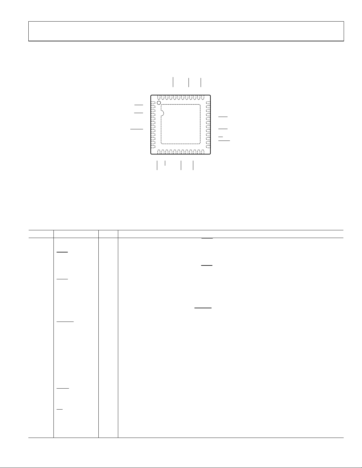
PIN CONFIGURATION AND FUNCTION DESCRIPTIONS
PLL1_OUT
LDO_PLL1
VDD3_PLL1
REF_SE L
ZD_IN
ZD_IN
VDD1.8_PLL2
OUT0
OUT0
VDD3_OUT[0:1]
OUT1
OUT1
41
39
43
42
44
45
46
47
48
37
40
38
1
REFA
2
REFA
3
REFB
4
REFB
OSC_IN
OSC_IN
5
6
7
8
9
10
11
12
LF1_EXT _CAP
OSC_CTRL
LF2_EXT _CAP
LDO_PLL2
VDD3_PLL2
LDO_VCO
NOTES
1. THE EXPOSED PADDLE IS A GROUND CONNECTION ON THE CHIP. IT MUST BE SOLDERED
TO THE ANALOG GROUND OF THE PCB TO ENSURE PROPER FUNCTIONALITY
AND HEAT DISSIPATION, NOISE, AND MECHANICAL STRENGTH BENEFITS.
15
14
13
CS
SYNC
VDD3_REF
AD9524
TOP
VIEW
(Not to Scale)
19
18
17
16
SDO
OUT5
SDIO/SDA
SCLK/SCL
21
20
OUT5
VDD3_OUT[4:5]
36
STATUS0/SP0
35
STATUS1/SP1
34
VDD1.8_OUT[0:3]
OUT2
33
32
OUT2
31
VDD3_OUT[2:3]
OUT3
30
29
OUT3
28
EEPROM_SEL
27
PD
RESET
26
25
REF_TEST
24
23
22
OUT4
OUT4
VDD1.8_OUT[ 4:5]
09081-002
Figure 2. Pin Configuration
Table 18. Pin Function Descriptions
Pin No. Mnemonic Type1 Description
1 REFA I
Reference Clock Input A. Along with REFA
, this pin is the differential input for the PLL reference.
Alternatively, this pin can be programmed as a single-ended 3.3 V CMOS input.
2
REFA
I
Complementary Reference Clock Input A. Along with REFA, this pin is the differential input for
the PLL reference. Alternatively, this pin can be programmed as a single-ended 3.3V CMOS input.
3 REFB I
Reference Clock Input B. Along with REFB
, this pin is the differential input for the PLL reference.
Alternatively, this pin can be programmed as a single-ended 3.3 V CMOS input.
4
REFB
I
Complementary Reference Clock Input B. Along with REFB, this pin is the differential input for
the PLL reference. Alternatively, this pin can be programmed as a single-ended 3.3 V CMOS input.
5 LF1_EXT_CAP O PLL1 External Loop Filter Capacitor. Connect this pin to ground.
6 OSC_CTRL O Oscillator Control Voltage. Connect to the voltage control pin of the external oscillator.
7 OSC_IN I
PLL1 Oscillator Input. Along with OSC_IN
, this pin is the differential input for the PLL reference.
Alternatively, this pin can be programmed as a single-ended 3.3 V CMOS input.
8
OSC_IN
I
Complementary PLL1 Oscillator Input. Along with OSC_IN, this pin is the differential input for the
PLL reference. Alternatively, this pin can be programmed as a single-ended 3.3 V CMOS input.
9 LF2_EXT_CAP O PLL2 External Loop Filter Capacitor. Connect this pin to the LDO_VCO pin.
10 LDO_PLL2 P/O
LDO Decoupling Pin for PLL2 1.8 V Internal Regulator. Connect a 0.47 F decoupling capacitor
from this pin to ground. Note that for best performance, the LDO bypass capacitor must be
placed in close proximity to the device.
11 VDD3_PLL2 P 3.3 V Supply for PLL2.
12 LDO_VCO P/O
2.5 V LDO Internal Regulator Decoupling Pin for VCO. Connect a 0.47 µF decoupling capacitor
from this pin to ground. Note that, for best performance, the LDO bypass capacitor must be
placed in close proximity to the device.
13
SYNC
I
Manual Synchronization. This pin initiates a manual synchronization and has an internal
40 kΩ pull-up resistor.
14 VDD3_REF P 3.3 V Supply for Output Clock Drivers Reference.
15
CS
16 SCLK/SCL I
I Serial Control Port Chip Select, Active Low. This pin has an internal 40 kΩ pull-up resistor.
2
Serial Control Port Clock Signal for SPI Mode (SCLK) or I
C Mode (SCL). Data clock for serial programming.
This pin has an internal 40 kΩ pull-down resistor in SPI mode but is high impedance in I²C mode.
17 SDIO/SDA I/O Serial Control Port Bidirectional Serial Data In/Out for SPI Mode (SDIO) or I²C Mode (SDA).
Rev. C | Page 13 of 56
AD9524
Pin No. Mnemonic Type1 Description
18 SDO O
19 OUT5 O
20 OUT5 O
21 VDD3_OUT[4:5] P 3.3 V Supply for Output 4 and Output 5 Clock Drivers.
22 OUT4 O
23 OUT4 O
24 VDD1.8_OUT[4:5] P 1.8 V Supply for Output 4 and Output 5 Clock Dividers.
25 REF_TEST I Test Input to PLL1 Phase Detector.
26 RESET I
27 PD Chip Power-Down, Active Low. This pin has an internal 40 kΩ pull-up resistor.
28 EEPROM_SEL I
29 OUT3 O
30 OUT3 O
31 VDD3_OUT[2:3] P 3.3 V Supply Output 2 and Supply Output 3 Clock Drivers.
32 OUT2 O
33 OUT2 O
34 VDD1.8_OUT[0:3] P 1.8 V Supply for Output 0, Output 1, Output 2, and Output 3 Clock Dividers.
35 STATUS1/SP1 I/O Lock Detect and Other Status Signals (STATUS1)/I2C Address (SP1).
36 STATUS0/SP0 I/O Lock Detect and Other Status Signals (STATUS0)/I2C Address (SP0).
37 OUT1 O
38 OUT1 O
39 VDD3_OUT[0:1] P 3.3 V Supply Output 0 and Supply Output 1 Clock Drivers.
40 OUT0 O
41 OUT0 O
42 VDD1.8_PLL2 P 1.8 V Supply for PLL2.
43 ZD_IN I External Zero Delay Clock Input. Along with ZD_IN, this pin is the differential input for the PLL
44 ZD_IN I
45 REF_SEL I Reference Input Select. This pin has an internal 40 kΩ pull-down resistor.
46 PLL1_OUT O
47 LDO_PLL1 P/O
48 VDD3_PLL1 P 3.3 V Supply PLL1. Use the same supply as VCXO.
EP EP, GND GND
1
P = power, I = input, O = output, I/O = input/output, P/O = power/output, GND = ground.
Serial Data Output. Use this pin to read data in 4-wire mode (high impedance in 3-wire mode).
There is no internal pull-up/pull-down resistor on this pin.
Complementary Clock Output 5. This pin can be configured as one side of a differential LVPECL/
LVDS/HSTL output or as a single-ended CMOS output.
Clock Output 5. This pin can be configured as one side of a differential LVPECL/LVDS/HSTL output
or as a single-ended CMOS output.
Complementary Clock Output 4. This pin can be configured as one side of a differential LVPECL/
LVDS/HSTL output or as a single-ended CMOS output.
Clock Output 4. This pin can be configured as one side of a differential LVPECL/LVDS/HSTL output
or as a single-ended CMOS output.
Digital Input, Active Low. Resets internal logic to default states. This pin has an internal
40 kΩ pull-up resistor.
EEPROM Select. Setting this pin high selects the register values stored in the internal EEPROM to
be loaded at reset and/or power-up. Setting this pin low causes the AD9524 to load the hardcoded default register values at power-up/reset. This pin has an internal 40 kΩ pull-down resistor.
Complementary Clock Output 3. This pin can be configured as one side of a differential LVPECL/
LVDS/HSTL output or as a single-ended CMOS output.
Square Wave Clocking Output 3. This pin can be configured as one side of a differential LVPECL/
LVDS/HSTL output or as a single-ended CMOS output.
Complementary Clock Output 2. This pin can be configured as one side of a differential LVPECL/
LVDS/HSTL output or as a single-ended CMOS output.
Clock Output 2. This pin can be configured as one side of a differential LVPECL/LVDS/HSTL output
or as a single-ended CMOS output.
Complementary Clock Output 1. This pin can be configured as one side of a differential LVPECL/
LVDS/HSTL output or as a single-ended CMOS output.
Clock Output 1. This pin can be configured as one side of a differential LVPECL/LVDS/HSTL output
or as a single-ended CMOS output.
Complementary Clock Output 0. This pin can be configured as one side of a differential LVPECL/
LVDS/HSTL output or as a single-ended CMOS output.
Clock Output 0. This pin can be configured as one side of a differential LVPECL/LVDS/HSTL output
or as a single-ended CMOS output.
reference. Alternatively, this pin can be programmed as a single-ended 3.3 V CMOS input.
Complementary External Zero Delay Clock Input. Along with ZD_IN, this pin is the differential input
for the PLL reference. Alternatively, this pin can be programmed as a single-ended 3.3 V CMOS input.
Single-Ended CMOS Output from PLL1. This pin has settings for weak and strong in
Register 0x1BA, Bit 4 (see Table 51).
1.8 V Internal LDO Regulator Decoupling Pin for PLL1. Connect a 0.47 µF decoupling capacitor
from this pin to ground. Note that, for best performance, the LDO bypass capacitor must be
placed in close proximity to the device.
Exposed Paddle. The exposed paddle is the ground connection on the chip. It must be soldered
to the analog ground of the PCB to ensure proper functionality and heat dissipation, noise, and
mechanical strength benefits.
Rev. C | Page 14 of 56
AD9524
TYPICAL PERFORMANCE CHARACTERISTICS
f
= 122.88 MHz, REFA differential at 30.72 MHz, f
VCXO
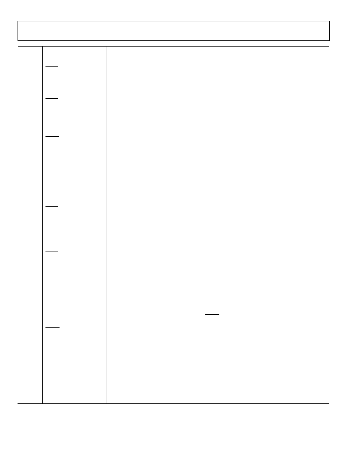
60
= 3686.4 MHz, and doubler is off, unless otherwise noted.
VCO
35
50
40
30
CURRENT (mA)
20
10
0
0 200 400 600 800 1000 1200
HSTL = 16m A
HSTL = 8mA
FREQUE NCY (MHz)
Figure 3. VDD3_OUT[x:y] Current (Typical) vs. Frequency;
HSTL Mode, 16 mA and 8 mA
45
40
35
30
25
20
CURRENT (mA)
15
10
5
0
0 200 400 600 800 1000 1200
LVD S = 7 mA
LVDS = 3.5mA
FREQUENCY ( MHz)
Figure 4. VDD3_OUT[x:y] Current (Typical) vs. Frequency;
LVDS Mode, 7 mA and 3.5 mA
30
25
20
15
CURRENT (mA)
10
5
0
0 100 200 300 400
09081-003
FREQUENCY ( MHz)
20pF
10pF
2pF
500
09081-006
Figure 6. VDD3_OUT[x:y] Current (Typical) vs. Frequency;
CMOS Mode, 20 pF, 10 pF, and 2 pF Load
3.5
3.0
2.5
2.0
1.5
1.0
DIFFERENTIAL SWING (V p-p)
0.5
0
0 200 400 600 800 1000 1200
09081-004
HSTL = 16mA
HSTL = 8mA
FREQUENCY (MHz)
09081-007
Figure 7. Differential Voltage Swing vs. Frequency;
HSTL Mode, 16 mA and 8 mA
45
40
35
30
25
20
CURRENT (mA)
15
10
5
0
0 200 400 600 800 1000 1200
FREQUENCY ( MHz)
Figure 5. VDD3_OUT[x:y] Current (Typical) vs. Frequency, LVPECL Mode
09081-005
Rev. C | Page 15 of 56
1.6
1.4
1.2
1.0
0.8
0.6
0.4
DIFFERENTIAL SWING (V p-p)
0.2
0
0 200 400 600 800 1000 1200
FREQUENCY (MHz)
Figure 8. Differential Voltage Swing vs. Frequency,
LVPECL Mode
09081-008
AD9524
A
–
–
1.4
1.2
LVD S = 7 mA
1.0
0.8
L SWING (V p-p)
0.6
LVDS = 3.5mA
0.4
DIFFERENTI
0.2
0
0200
400 600 800 1000 1200
FREQUENCY (M Hz)
Figure 9. Differential Voltage Swing vs. Frequency;
LVDS Mode, 7 mA and 3.5 mA
09081-009
–80
–90
–100
–110
70
1
1: 100Hz, –85.0688dBc/Hz
2: 1kHz, –113.3955dBc/Hz
3: 8kHz, –125.8719dBc/Hz
4: 16kHz, –129.5942dBc/Hz
5: 100kHz, –134.5017dBc/Hz
6: 1MHz, –145.2872dBc/Hz
7: 10MHz, –156.2706dBc/Hz
8: 40MHz, –157.4153dBc/Hz
x: START 12kHz
CENTER 40.006MHz
SPAN 79.988MHz
–120
–130
–140
PHASE NOISE (dBc/Hz)
NOISE:
ANALYSIS RANG E X: BAND M ARKER
ANALYSIS RANG E Y: BAND M ARKER
–150
INTG NOISE: –75.94595dBc/39.99MHz
RMS NOISE: 225.539µRAD
12.9224mdeg
–160
RMS JITTER: 194.746fsec
RESIDUAL FM: 2.81623kHz
–170
100 1k 10k 100k 1M 10M
3
5
FREQUENCY (Hz)
Figure 12. Phase Noise, Output = 184.32 MHz
(VCXO = 122.88 MHz, Crystek VCXO CVHD-950)
STOP 80MHz
7
09081-015
3.5
2pF
3.3
3.1
10pF
2.9
2.7
20pF
2.5
AMPLITUDE (V)
2.3
2.1
1.9
1.7
0 100 200 300 400
FREQUENCY ( MHz)
Figure 10. Amplitude vs. Frequency and Capacitive Load;
CMOS Mode, 2 pF, 10 pF, and 20 pF
1
500
–80
–90
–100
–110
70
1
1: 100Hz, –89.0260dBc/Hz
2: 1kHz, –116.9949dBc/Hz
3: 8kHz, –129.5198dBc/Hz
4: 16kHz, –133.3916dBc/Hz
5: 100kHz, –137.7680dBc/Hz
6: 1MHz, –148.3519dBc/Hz
7: 10MHz, –158.3307dBc/Hz
8: 40MHz, 159.1629–dBc/Hz
x: START 12kHz
STOP 80MHz
CENTER 40.006MHz
SPAN 79.988MHz
–120
–130
–140
PHASE NOISE (dBc/Hz)
NOISE:
ANALYSIS RANG E X: BAND M ARKER
ANALYSIS RANG E Y: BAND M ARKER
–150
INTG NOISE: –78.8099dBc/39.99MHz
RMS NOISE: 162.189µRAD
9.29276mdeg
–160
RMS JITTER: 210.069fsec
RESIDUAL FM: 2.27638kHz
–170
100 1k 10k 100k 1M 10M
09081-010
3
5
FREQUENCY (Hz)
7
09081-016
Figure 13. Phase Noise, Output = 122.88 MHz
(VCXO = 122.88 MHz, Crystek VCXO CVHD-950; Doubler Is Off)
1
CH1 200mV 2.5ns/DI V
40.0GS/s
Figure 11. Output Waveform (Differential), LVPECL at 122.88 MHz
A CH1 104mV
09081-013
CH1 500mV Ω 2.5ns/ DIV
40.0GS/s
A CH1 80mV
09081-017
Figure 14. Output Waveform (Differential), HSTL at 16 mA, 122.88 MHz
Rev. C | Page 16 of 56
AD9524
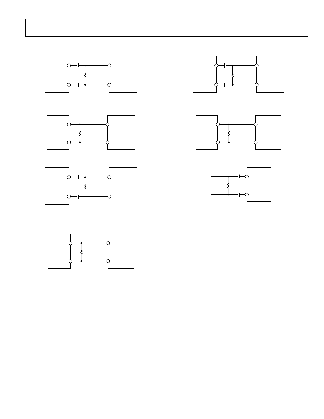
INPUT/OUTPUT TERMINATION RECOMMENDATIONS
AD9524
LVD S
OUTPUT
0.1µF
100Ω
0.1µF
HIGH
IMPEDANCE
INPUT
Figure 15. AC-Coupled LVDS Output Driver
AD9524
LVD S
OUTPUT
100Ω
HIGH
IMPEDANCE
INPUT
Figure 16. DC-Coupled LVDS Output Driver
AD9524
LVP ECL -
COMPATIBLE
OUTPUT
0.1µF
100Ω
0.1µF
HIGH
IMPEDANCE
INPUT
Figure 17. AC-Coupled LVPECL Output Driver
DOWNSTREAM
DEVICE
DOWNSTREAM
DEVICE
DOWNSTREAM
DEVICE
AD9524
HSTL
OUTPUT
09081-142
0.1µF
100Ω
0.1µF
HIGH
IMPEDANCE
INPUT
DOWNST REAM
DEVICE
09081-046
Figure 19. AC-Coupled HSTL Output Driver
AD9524
HSTL
OUTPUT
09081-143
100Ω
HIGH
IMPEDANCE
INPUT
DOWNSTREAM
DEVICE
09081-047
Figure 20. DC-Coupled HSTL Output Driver
0.1µF
100Ω
1
(OPTIONAL
09081-044
1
RESISTOR VALUE DEPENDS UPON
REQUIRED TERMINATION OF SOURCE.
)
0.1µF
AD9524
SELF-BIASED
REF, VCXO,
ZERO DELAY
INPUTS
09081-048
Figure 21. REF, VCXO, and Zero Delay Input, Differential Mode (When In
CMOS Single-Ended Input Mode, the Unused Input Can Be Left Unconnected)
AD9524
LVPECL-
COMPATIBLE
OUTPUT
100Ω
HIGH
IMPEDANCE
INPUT
DOWNSTREAM
DEVICE
09081-045
Figure 18. DC-Coupled LVPECL Output Driver
Rev. C | Page 17 of 56
 Loading...