Analog Devices AD9248 a Datasheet
14-Bit, 20 MSPS/40 MSPS/65 MSPS
FEATURES
Integrated dual 14-bit ADC
Single 3 V supply operation (2.7 V to 3.6 V)
SNR = 71.6 dB (to Nyquist, AD9248-65)
SFDR = 80.5 dBc (to Nyquist, AD9248-65)
Low power: 300 mW/channel at 65 MSPS
Differential input with 500 MHz, 3 dB bandwidth
Exceptional crosstalk immunity > 85 dB
Flexible analog input: 1 V p-p to 2 V p-p range
Offset binary or twos complement data format
Clock duty cycle stabilizer
Output datamux option
APPLICATIONS
Ultrasound equipment
Direct conversion or IF sampling receivers
WB-CDMA, CDMA2000,WiMAX
Battery-powered instruments
Hand-held scopemeters
Low cost digital oscilloscopes
GENERAL DESCRIPTION
The AD9248 is a dual, 3 V, 14-bit, 20 MSPS/40 MSPS/65 MSPS
analog-to-digital converter (ADC). It features dual high
performance sample-and hold amplifiers (SHAs) and an
integrated voltage reference. The AD9248 uses a multistage
differential pipelined architecture with output error correction
logic to provide 14-bit accuracy and to guarantee no missing
codes over the full operating temperature range at up to
65 MSPS data rates. The wide bandwidth, differential SHA
allows for a variety of user-selectable input ranges and offsets,
including single-ended applications. It is suitable for various
applications, including multiplexed systems that switch fullscale voltage levels in successive channels and for sampling
inputs at frequencies well beyond the Nyquist rate.
Dual single-ended clock inputs are used to control all internal
conversion cycles. A duty cycle stabilizer is available and can
compensate for wide variations in the clock duty cycle, allowing
the converter to maintain excellent performance. The digital
output data is presented in either straight binary or twos
complement format. Out-of-range signals indicate an overflow
condition, which can be used with the most significant bit to
determine low or high overflow.
Rev. A
Information furnished by Analog Devices is believed to be accurate and reliable.
However, no responsibility is assumed by Analog Devices for its use, nor for any
infringements of patents or other rights of third parties that may result from its use.
Specifications subject to change without notice. No license is granted by implication
or otherwise under any patent or patent rights of Analog Devices. Trademarks and
registered trademarks are the property of their respective owners.
Dual A/D Converter
AD9248
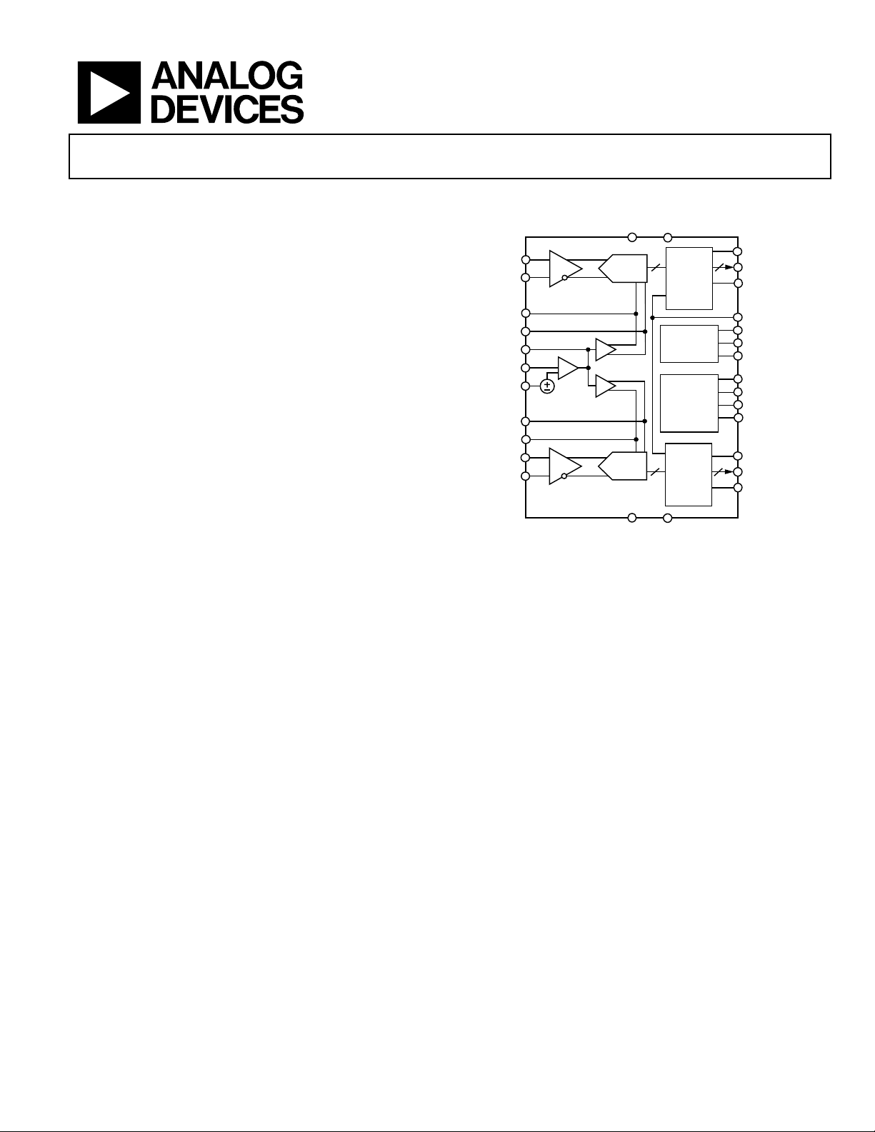
FUNCTIONAL BLOCK DIAGRAM
AVDD
AGND
VIN+_A
VIN–_A
REFT_A
REFB_A
VREF
SENSE
AGND
REFT_B
REFB_B
VIN+_B
VIN–_B
SHA
0.5V
SHA
AD9248
Fabricated on an advanced CMOS process, the AD9248 is
available in a Pb-free, space saving, 64-lead LQFP or LFCSP and
is specified over the industrial temperature range (−40°C to
+85°C).
PRODUCT HIGHLIGHTS
1. Pin-compatible with the AD9238, 12-bit 20 MSPS/
40 MSPS/65 MSPS ADC.
2. Speed grade options of 20 MSPS, 40 MSPS, and 65 MSPS
allow flexibility between power, cost, and performance to suit
an application.
3. Low power consumption: AD9248-65: 65 MSPS = 600 mW,
AD9248-40: 40 MSPS = 330 mW, and AD9248-20: 20 MSPS
= 180 mW.
4. Typical channel isolation of 85 dB @ f
5. The clock duty cycle stabilizer (AD9248-20/AD9248-40/
AD9248-65) maintains performance over a wide range of
clock duty cycles.
6. Multiplexed data output option enables single-port operation
from either Data Port A or Data Port B.
One Technology Way, P.O. Box 9106, Norwood, MA 02062-9106, U.S.A.
Tel: 781.329.4700
Fax: 781.461.3113
www.analog.com
©2005 Analog Devices, Inc. All rights reserved.
ADC
ADC
DRVDD
Figure 1.
14
OUTPUT
MUX/
BUFFERS
CLOCK
DUTY CYCLE
STABILIZER
MODE
CONTROL
OUTPUT
MUX/
BUFFERS
DRGND
14
1414
= 10 MHz.
IN
OTR_A
D13_A TO D0_A
OEB_A
MUX_SELECT
CLK_A
CLK_B
DCS
SHARED_REF
PWDN_A
PWDN_B
DFS
OTR_B
D13_B TO D0_B
OEB_B
04446-001

AD9248
TABLE OF CONTENTS
Specifications..................................................................................... 3
Clock Circuitry ........................................................................... 22
DC Specifications ......................................................................... 3
AC Specifications.......................................................................... 5
Digital Specifications ................................................................... 6
Switching Specifications .............................................................. 7
Absolute Maximum Ratings............................................................ 8
Explanation of Test Levels........................................................... 8
ESD Caution.................................................................................. 8
Pin Configuration and Function Descriptions............................. 9
Te r mi n ol o g y .................................................................................... 11
Typical Performance Characteristics ........................................... 12
Equivalent Circuits......................................................................... 16
Theory of Operation ...................................................................... 17
Analog Input ............................................................................... 17
Clock Input and Considerations .............................................. 18
Power Dissipation and Standby Mode..................................... 19
Analog Inputs ............................................................................. 22
Reference Circuitry .................................................................... 22
Digital Control Logic................................................................. 22
Outputs ........................................................................................ 22
LQFP Evaluation Board Bill of Materials (BOM) .................. 24
LQFP Evaluation Board Schematics........................................ 25
LQFP PCB Layers....................................................................... 29
Dual ADC LFCSP PCB.................................................................. 35
Power Connector ........................................................................ 35
Analog Inputs ............................................................................. 35
Optional Operational Amplifier .............................................. 35
Clock ............................................................................................ 35
Volt a ge R e fere n ce ....................................................................... 35
Data Outputs............................................................................... 35
LFCSP Evaluation Board Bill of Materials (BOM) ................ 36
Digital Outputs ........................................................................... 19
Timing.......................................................................................... 19
Data Format ................................................................................ 20
Voltage Reference....................................................................... 20
AD9248 LQFP Evaluation Board .................................................22
REVISION HISTORY
3/05—Rev. 0 to Rev. A
Added LFCSP......................................................................Universal
Changes to Features.......................................................................... 1
Changes to Applications .................................................................. 1
Changes to General Description .................................................... 1
Changes to Product Highlights....................................................... 1
Changes to Table 6.......................................................................... 10
Changes to Terminology................................................................ 11
Changes to Figure 22...................................................................... 15
Changes to Clock Input and Considerations Section ................ 18
Changes to Timing Section ........................................................... 19
LFCSP PCB Schematics............................................................. 37
LFCSP PCB Layers..................................................................... 40
Thermal Considerations............................................................ 45
Outline Dimensions ....................................................................... 46
Ordering Guide .......................................................................... 47
Changes to Figure 33...................................................................... 19
Changes to Data Format Section.................................................. 20
Changes to Table 10 ....................................................................... 24
Changes to Figure 39...................................................................... 25
Changes to Table 13 ....................................................................... 36
Updated Outline Dimensions....................................................... 46
Changes to Ordering Guide.......................................................... 47
1/05—Revision 0: Initial Version
Rev. A | Page 2 of 48

AD9248
SPECIFICATIONS
DC SPECIFICATIONS
AVDD = 3 V, DRVDD = 2.5 V, maximum sample rate, CLK_A = CLK_B; AIN = −0.5 dBFS differential input, 1.0 V internal reference,
to T
T
MIN
Table 1.
Parameter Temp Level Min Typ Max Min Typ Max Min Typ Max Unit
RESOLUTION Full VI 14 14 14 Bits
ACCURACY
No Missing Codes Guaranteed Full VI 14 14 14 Bits
Offset Error 25°C I ±0.2 ±1.3 ±0.2 ±1.3 ±0.2 ±1.3 % FSR
Gain Error
Differential Nonlinearity (DNL)
25°C IV ±0.6 ±1.0 ±0.6 ±1.0 ±0.65 ±1.0 LSB
Integral Nonlinearity (INL)2 Full V ±2.7 ±2.7 ±2.8 LSB
25°C IV ±2.3 ±4.5 ±2.3 ±4.5 ±2.4 ±4.5 LSB
TEMPERATURE DRIFT
Offset Error Full V ±2 ±2 ±3 ppm/°C
Gain Error1 Full V ±12 ±12 ±12 ppm/°C
INTERNAL VOLTAGE REFERENCE
Output Voltage Error (1 V Mode) Full VI ±5 ±35 ±5 ±35 ±5 ±35 mV
Load Regulation @ 1.0 mA Full V 0.8 0.8 0.8 mV
Output Voltage Error (0.5 V Mode) Full V ±2.5 ±2.5 ±2.5 mV
Load Regulation @ 0.5 mA Full V 0.1 0.1 0.1 mV
INPUT REFERRED NOISE
Input Span = 1 V 25°C V 2.1 2.1 2.1 LSB
Input Span = 2.0 V 25°C V 1.05 1.05 1.05 LSB
ANALOG INPUT
Input Span = 1.0 V Full IV 1 1 1 V p-p
Input Span = 2.0 V Full IV 2 2 2 V p-p
Input Capacitance
REFERENCE INPUT RESISTANCE Full V 7 7 7 kΩ
POWER SUPPLIES
Supply Voltages
Supply Current
PSRR Full V ±0.01 ±0.01 ±0.01 % FSR
POWER CONSUMPTION
DC Input
Sine Wave Input2 Full VI 190 217 360 400 640 700 mW
Standby Power
, DCS enabled, unless otherwise noted.
MAX
Test AD9248BST/BCP-20 AD9248BST/BCP-40 AD9248BST/BCP-65
1
3
Full IV ±0.25 ±2.2 ±0.3 ±2.4 ±0.5 ±2.5 % FSR
2
Full V ±0.65 ±0.65 ±0.7 LSB
Full V 7 7 7 pF
rms
rms
AVDD Full IV 2.7 3.0 3.6 2.7 3.0 3.6 2.7 3.0 3.6 V
DRVDD Full IV 2.25 3.0 3.6 2.25 3.0 3.6 2.25 3.0 3.6 V
IAVDD2 Full V 60 110 200 mA
IDRVDD2 Full V 5 11 16 mA
4
5
Full V 180 330 600 mW
Full V 2.0 2.0 2.0 mW
Rev. A | Page 3 of 48
AD9248
Test AD9248BST/BCP-20 AD9248BST/BCP-40 AD9248BST/BCP-65
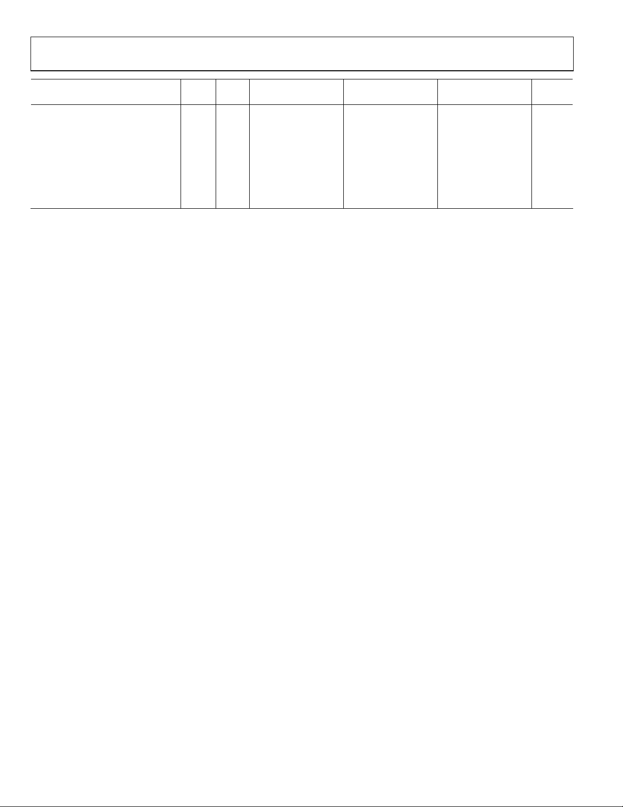
Parameter Temp Level Min Typ Max Min Typ Max Min Typ Max Unit
MATCHING CHARACTERISTICS
Offset Error
25°C I ±0.19 ±1.56 ±0.19 ±1.56 ±0.25 ±1.74 % FSR
(Nonshared Reference Mode)
Offset Error
25°C I ±0.19 ±1.56 ±0.19 ±1.56 ±0.25 ±1.74 % FSR
(Shared Reference Mode)
Gain Error
25°C I ±0.07 ±1.43 ±0.07 ±1.43 ±0.07 ±1.47 % FSR
(Nonshared Reference Mode)
Gain Error
25°C I ±0.01 ±0.06 ±0.01 ±0.06 ±0.01 ±0.10 % FSR
(Shared Reference Mode)
1
Gain error and gain temperature coefficient are based on the ADC only (with a fixed 1.0 V external reference).
2
Measured at maximum clock rate with a low frequency sine wave input and approximately 5 pF loading on each output bit.
3
Input capacitance refers to the effective capacitance between one differential input pin and AVSS. Refer to Figure for the equivalent analog input structure. 28
4
Measured with dc input at maximum clock rate.
5
Standby power is measured with the CLK_A and CLK_B pins inactive (that is, set to AVDD or AGND).
Rev. A | Page 4 of 48

AD9248
AC SPECIFICATIONS
AVDD = 3 V, DRVDD = 2.5 V, maximum sample rate, CLK_A = CLK_B; AIN = −0.5 dBFS differential input, 1.0 V external reference,
to T
T
MIN
Table 2.
Parameter Temp Level Min Typ Max Min Typ Max Min Typ Max Unit
SIGNAL-TO-NOISE RATIO (SNR)
f
INPUT
25°C IV 73.1 73.7 72.8 73.4 72.3 73.1 dB
f
INPUT
25°C IV 72.4 73.1 dB
f
INPUT
25°C IV 72.3 72.9 dB
f
INPUT
25°C IV 71.2 71.6 dB
f
INPUT
SIGNAL-TO-NOISE AND DISTORTION
RATIO (SINAD)
f
INPUT
25°C IV 72.2 73.2 72.0 73.0 71.7 72.7 dB
f
INPUT
25°C IV 70.9 72.2 dB
f
INPUT
25°C IV 71.0 72.3 dB
f
INPUT
25°C IV 70.0 71.0 dB
f
INPUT
EFFECTIVE NUMBER OF BITS (ENOB)
f
INPUT
25°C IV 11.7 11.8 11.7 11.8 11.6 11.8 Bits
f
INPUT
25°C IV 11.5 11.7 Bits
f
INPUT
25°C IV 11.5 11.7 Bits
f
INPUT
25°C IV 11.3 11.5 Bits
f
INPUT
WORST HARMONIC (SECOND or THIRD)
f
INPUT
25°C IV 77.5 87.5 77.5 86.0 77.5 86.0 dBc
f
INPUT
25°C I 76.1 84.0 dBc
f
INPUT
25°C I 76.0 84.0 dBc
f
INPUT
25°C I 73.0 80.5 dBc
, DCS Enabled, unless otherwise noted.
MAX
Test AD9248BST/BCP-20 AD9248BST/BCP-40 AD9248BST/BCP-65
= 2.4 MHz Full V 73.4 73.1 72.8 dB
= 9.7 MHz Full V 72.9 dB
= 19.6 MHz Full V 72.7 dB
= 35 MHz Full V 71.5 dB
= 100 MHz 25°C V 70 69.5 69.0 dB
= 2.4 MHz Full V 73.0 72.8 72.5 dB
= 9.7 MHz Full V 72.0 dB
= 19.6 MHz Full V 72.1 dB
= 35 MHz Full V 70.9 dB
= 100 MHz 25°C V 69.5 69.0 68.5 dB
= 2.4 MHz Full V 11.8 11.8 11.8 Bits
= 9.7 MHz Full V 11.7 Bits
= 19.6 MHz Full V 11.7 Bits
= 35 MHz Full V 11.5 Bits
= 100 MHz 25°C V 11.3 11.2 11.2 Bits
= 2.4 MHz Full V 86.0 85.0 84.0 dBc
= 9.7 MHz Full V 83.0 dBc
= 19.6 MHz Full V 83.0 dBc
= 35 MHz Full V 80.0 dBc
Rev. A | Page 5 of 48

AD9248
Test AD9248BST/BCP-20 AD9248BST/BCP-40 AD9248BST/BCP-65
Parameter Temp Level Min Typ Max Min Typ Max Min Typ Max Unit
WORST OTHER SPUR
(NONSECOND or THIRD)
f
= 2.4 MHz Full V 88.0 88.0 85.5 dBc
INPUT
25°C I 83.3 89.0 83.5 89.0 81.0 86.0 dBc
f
= 9.7 MHz Full V 87.0 dBc
INPUT
25°C I 83.1 88.0 dBc
f
= 19.6 MHz Full V 88.0 dBc
INPUT
25°C I 82.6 88.5 dBc
f
= 35 MHz Full V 85.5 dBc
INPUT
25°C I 79.8 86.0 dBc
f
= 100 MHz 25°C V 79.0 81.0 75.0 dBc
INPUT
SPURIOUS-FREE DYNAMIC RANGE (SFDR)
f
= 2.4 MHz Full V 86.0 85.0 84.0 dBc
INPUT
25°C IV 77.5 87.5 77.5 86.0 77.5 86.0 dBc
f
= 9.7 MHz Full V 83.0 dBc
INPUT
25°C I 76.1 84.0 dBc
f
= 19.6 MHz Full V 83.0 dBc
INPUT
25°C I 76.0 84.0 dBc
f
= 35 MHz Full V 80.0 dBc
INPUT
25°C I 73.0 80.5 dBc
CROSSTALK Full V −85.0 −85.0 −85.0 dB
DIGITAL SPECIFICATIONS
AVDD = 3 V, DRVDD = 2.5 V, maximum sample rate, CLK_A = CLK_B; AIN = −0.5 dBFS differential input, 1.0 V internal reference,
to T
T
MIN
Table 3.
Parameter Temp Level Min Typ Max Min Typ Max Min Typ Max Unit
LOGIC INPUTS
High Level Input Voltage Full IV 2.0 2.0 2.0 V
Low Level Input Voltage Full IV 0.8 0.8 0.8 V
High Level Input Current Full IV −10 +10 −10 +10 −10 +10 µA
Low Level Input Current Full IV −10 +10 −10 +10 −10 +10 µA
Input Capacitance Full IV 2 2 2 pF
LOGIC OUTPUTS
High Level Output Voltage Full IV
Low Level Output Voltage Full IV 0.05 0.05 0.05 V
1
Output voltage levels measured with capacitive load only on each output.
, DCS enabled, unless otherwise noted.
MAX
Test AD9248BST/BCP-20 AD9248BST-40 AD9248BST-65
1
DRVDD −
0.05
DRVDD −
0.05
DRVDD −
0.05
V
Rev. A | Page 6 of 48
AD9248
A
SWITCHING SPECIFICATIONS
AVDD = 3 V, DRVDD = 2.5 V, maximum sample rate, CLK_A = CLK_B; AIN = −0.5 dBFS differential input, 1.0 V internal reference,
to T
T
MIN
Table 4.
Parameter Temp Level Min Typ Max Min Typ Max Min Typ Max Unit
SWITCHING PERFORMANCE
Maximum Conversion Rate Full VI 20 40 65 MSPS
Minimum Conversion Rate Full V 1 1 1 MSPS
CLK Period Full V 50.0 25.0 15.4 ns
CLK Pulse-Width High
CLK Pulse-Width Low1 Full V 15.0 8.8 6.2 ns
DATA OUTPUT PARAMETER
Output Delay2 (tPD) Full VI 2 3.5 6 2 3.5 6 2 3.5 6 ns
Pipeline Delay (Latency) Full V 7 7 7 Cycles
Aperture Delay (tA) Full V 1.0 1.0 1.0 ns
Aperture Uncertainty (tJ) Full V 0.5 0.5 0.5 ps rms
Wake-Up Time
OUT-OF-RANGE RECOVERY TIME Full V 2 2 2 Cycles
1
The AD9248-65 model has a duty cycle stabilizer circuit that, when enabled, corrects for a wide range of duty cycles (see Figure 23).
2
Output delay is measured from clock 50% transition to data 50% transition, with a 5 pF load on each output.
3
Wake-up time is dependent on the value of the decoupling capacitors; typical values shown with 0.1 µF and 10 µF capacitors on REFT and REFB.
, DCS enabled, unless otherwise noted.
MAX
1
3
Full V 15.0 8.8 6.2 ns
Full V 2.5 2.5 2.5 Ms
Test AD9248BST/BCP-20 AD9248BST/BCP-40 AD9248BST/BCP-65
N–7
N+1
N+2
N+3
N–6
N–5
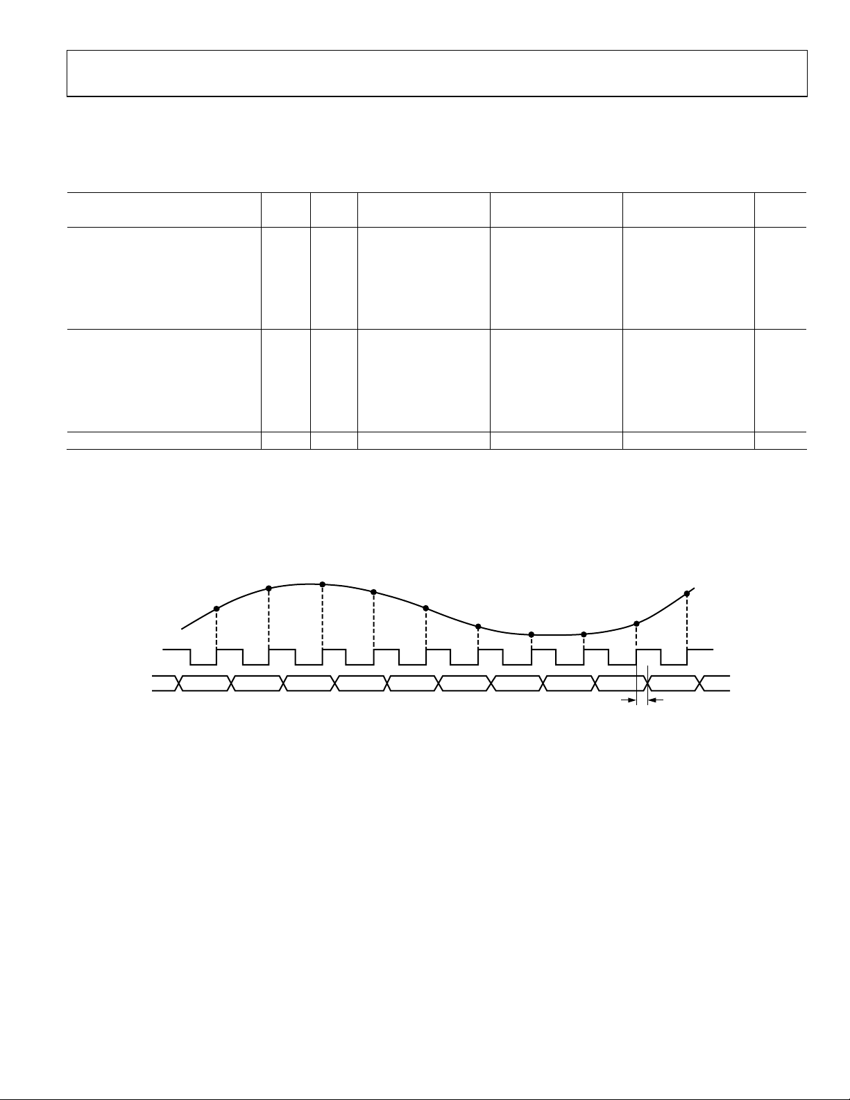
Figure 2. Timing Diagram
N–4
N+4
N–3
N+5
N–2
N+6
N–1
N+7
N
t
PD
N+8
=
MIN 2.0ns,
MAX 6.0ns
04446-002
NALOG
INPUT
CLOCK
DATA
OUT
N–9
N
N–1
N–8
Rev. A | Page 7 of 48
AD9248
ABSOLUTE MAXIMUM RATINGS
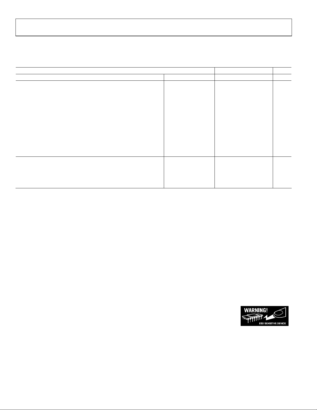
Table 5.
Parameter Rating
Pin Name With Respect To Min Max Unit
ELECTRICAL
AVDD AGND −0.3 +3.9 V
DRVDD DRGND −0.3 +3.9 V
AGND DRGND −0.3 +0.3 V
AVDD DRVDD −3.9 +3.9 V
Digital Outputs CLK, DCS, MUX_SELECT, SHARED_REF DRGND −0.3 DRVDD + 0.3 V
OEB, DFS AGND −0.3 AVDD + 0.3 V
VINA, VINB AGND −0.3 AVDD + 0.3 V
VREF AGND −0.3 AVDD + 0.3 V
SENSE AGND −0.3 AVDD + 0.3 V
REFB, REFT AGND −0.3 AVDD + 0.3 V
PDWN AGND −0.3 AVDD + 0.3 V
ENVIRONMENTAL
Operating Temperature −45 +85 °C
Junction Temperature 150 °C
Lead Temperature (10 sec) 300 °C
Storage Temperature −65 +150 °C
1
Absolute maximum ratings are limiting values to be applied individually, and beyond which the serviceability of the circuit may be impaired. Functional operability is
not necessarily implied. Exposure to absolute maximum rating conditions for an extended period of time may affect device reliability.
2
Typical thermal impedances: 64-lead LQFP, θJA = 54°C/W; 64-lead LFCSP, θJA = 26.4°C/W with heat slug soldered to ground plane. These measurements were taken on a
4-layer board in still air, in accordance with EIA/JESD51-7.
2
1
EXPLANATION OF TEST LEVELS
I 100% production tested.
II 100% production tested at 25°C and sample tested at specified temperatures.
III Sample tested only.
IV Parameter is guaranteed by design and characterization testing.
V Parameter is a typical value only.
VI
100% production tested at 25°C; guaranteed by design and characterization testing for industrial temperature range; 100% production
tested at temperature extremes for military devices.
ESD CAUTION
ESD (electrostatic discharge) sensitive device. Electrostatic charges as high as 4000 V readily accumulate
on the human body and test equipment and can discharge without detection. Although this product features
proprietary ESD protection circuitry, permanent damage may occur on devices subjected to high energy
electrostatic discharges. Therefore, proper ESD precautions are recommended to avoid performance
degradation or loss of functionality.
Rev. A | Page 8 of 48
AD9248
PIN CONFIGURATION AND FUNCTION DESCRIPTIONS
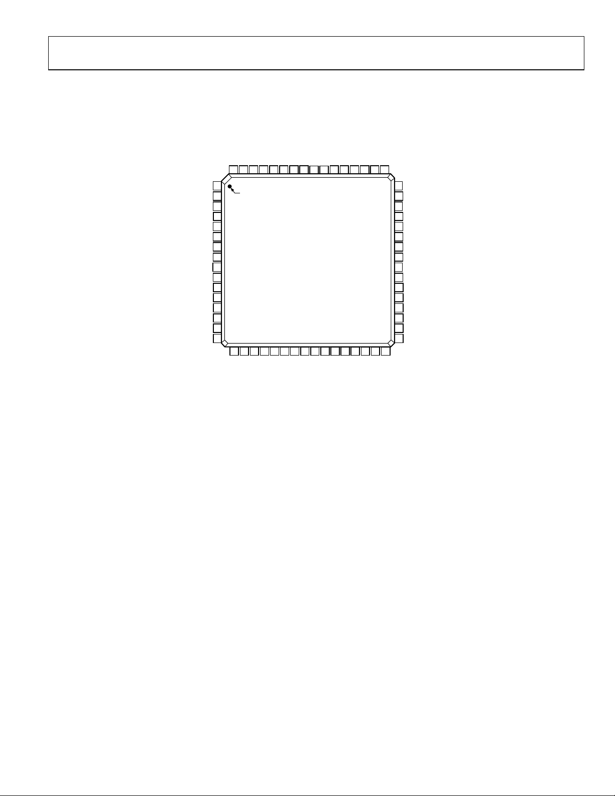
AVDD63CLK_A62SHARED_REF61MUX_SELECT60PDWN_A59OEB_A58OTR_A57D13_A (MSB)56D12_A55D11_A54D10_A53DRGND52DRVDD51D9_A50D8_A49D7_A
64
AGND
VIN+_A
VIN–_A
AGND
AVDD
REFT_A
REFB_A
VREF
SENSE
REFB_B
REFT_B
AVDD
AGND
VIN–_B
VIN+_B
AGND
1
PIN 1
2
3
4
5
6
7
8
9
10
11
12
13
14
15
16
17
18
19
20
21
22
AD9248
TOP VIEW
(Not to Scale)
23
24
28
29
30
48
D6_A
47
D5_A
46
D4_A
45
D3_A
44
D2_A
43
D1_A
42
D0_A (LSB)
41
DRVDD
40
DRGND
39
OTR_B
38
D13_B (MSB)
37
D12_B
36
D11_B
35
D10_B
34
D9_B
33
D8_B
AVDD
DCS
CLK_B
PDWN_B
OEB_B
D0_B (LSB)
D1_B25D2_B26D3_B27D4_B
DRVDD
DRGND
D5_B31D6_B32D7_B
DFS
Figure 3. Pin Configuration (64-Lead LQFP and 64-Lead LFCSP)
04446-003
Rev. A | Page 9 of 48

AD9248
Table 6. Pin Function Descriptions (64-Lead LQFP and 64-Lead LFCSP)
Pin No. Mnemonic Description
1, 4, 13, 16 AGND Analog Ground.
2 VIN+_A Analog Input Pin (+) for Channel A.
3 VIN−_A Analog Input Pin (−) for Channel A.
5, 12, 17, 64 AVDD Analog Power Supply.
6 REFT_A Differential Reference (+) for Channel A.
7 REFB_A Differential Reference (−) for Channel A.
8 VREF Voltage Reference Input/Output.
9 SENSE Reference Mode Selection.
10 REFB_B Differential Reference (−) for Channel B.
11 REFT_B Differential Reference (+) for Channel B.
14 VIN−_B Analog Input Pin (−) for Channel B.
15 VIN+_B Analog Input Pin (+) for Channel B.
18 CLK_B Clock Input Pin for Channel B.
19 DCS Enable Duty Cycle Stabilizer (DCS) Mode.
20 DFS Data Output Format Select Pin (Low for Offset Binary, High for Twos Complement).
21 PDWN_B
22 OEB_B
23 to 27,
30 to 38
28, 40, 53 DRGND Digital Output Ground.
29, 41, 52 DRVDD
39 OTR_B Out-of-Range Indicator for Channel B.
42 to 51,
54 to 57
58 OTR_A Out-of-Range Indicator for Channel A.
59 OEB_A
60 PDWN_A
61 MUX_SELECT
62 SHARED_REF Shared Reference Control Pin (Low for Independent Reference Mode, High for Shared Reference Mode).
63 CLK_A Clock Input Pin for Channel A.
D0_B (LSB) to
D13_B (MSB)
D0_A (LSB) to
D13_A (MSB)
Power-Down Function Selection for Channel B.
Logic 0 enables Channel B. Logic 1 powers down Channel B (outputs static, not High-Z).
Output Enable Pin for Channel B.
Logic 0 enables Data Bus B. Logic 1 sets outputs to High-Z.
Channel B Data Output Bits.
Digital Output Driver Supply. Must be decoupled to DRGND with a minimum 0.1 µF capacitor.
Recommended decoupling is 0.1 µF capacitor in parallel with 10 µF capacitor.
Channel A Data Output Bits.
Output Enable Pin for Channel A.
Logic 0 enables Data Bus A. Logic 1 sets outputs to High-Z.
Power-Down Function Selection for Channel A
Logic 0 enables Channel A. Logic 1 powers down Channel A (outputs static, not High-Z).
Data Multiplexed Mode.
(See Data Format section for how to enable; high setting disables output data multiplexed mode.)
Rev. A | Page 10 of 48

AD9248
TERMINOLOGY
Aperture Delay
SHA performance measured from the rising edge of the clock
input to when the input signal is held for conversion.
Aperture Jitter
The variation in aperture delay for successive samples, which is
manifested as noise on the input to the ADC.
Integral Nonlinearity (INL)
Deviation of each individual code from a line drawn from
negative full scale through positive full scale. The point used as
negative full scale occurs ½ LSB before the first code transition.
Positive full scale is defined as a level 1½ LSB beyond the last
code transition. The deviation is measured from the middle of
each particular code to the true straight line.
Differential Nonlinearity (DNL, No Missing Codes)
An ideal ADC exhibits code transitions that are exactly 1 LSB
apart. DNL is the deviation from this ideal value. Guaranteed
no missing codes to 14-bit resolution indicates that all 16,384
codes must be present over all operating ranges.
Offset Error
The major carry transition should occur for an analog value
½ LSB below VIN+ = VIN−. Offset error is defined as the
deviation of the actual transition from that point.
Gain Error
The first code transition should occur at an analog value ½ LSB
above negative full scale. The last transition should occur at an
analog value 1½ LSB below the nominal full scale. Gain error is
the deviation of the actual difference between first and last code
transitions and the ideal difference between first and last code
transitions.
Temp er at u re D ri ft
The temperature drift for zero error and gain error specifies the
maximum change from the initial (25°C) value to the value at
or T
T
MIN
MAX
.
Power Supply Rejection
The specification shows the maximum change in full scale from
the value with the supply at the minimum limit to the value
with the supply at its maximum limit.
Total Harmonic Distortion (THD)
The ratio of the rms sum of the first six harmonic components
to the rms value of the measured input signal, expressed as a
percentage or in decibels relative to the peak carrier signal (dBc).
Signal-to-Noise and Distortion (SINAD) Ratio
The ratio of the rms value of the measured input signal to the
rms sum of all other spectral components below the Nyquist
frequency, including harmonics but excluding dc. The value for
SINAD is expressed dB.
Effective Number of Bits (ENOB)
Using the following formula
ENOB = (SINAD − 1.76)/6.02
ENOB for a device for sine wave inputs at a given input
frequency can be calculated directly from its measured SINAD.
Signal-to-Noise Ratio (SNR)
The ratio of the rms value of the measured input signal to the
rms sum of all other spectral components below the Nyquist
frequency, excluding the first six harmonics and dc. The value
for SNR is expressed in dB.
Spurious-Free Dynamic Range (SFDR)
The difference in dB between the rms amplitude of the input
signal and the peak spurious signal.
Nyquist Sampling
When the frequency components of the analog input are below
the Nyquist frequency (f
/2), this is often referred to as
CLOCK
Nyquist sampling.
IF Sampling
Due to the effects of aliasing, an ADC is not limited to Nyquist
sampling. Higher sampled frequencies are aliased down into the
first Nyquist zone (DC − f
/2) on the output of the ADC.
CLOCK
The bandwidth of the sampled signal should not overlap
Nyquist zones and alias onto itself. Nyquist sampling
performance is limited by the bandwidth of the input SHA and
clock jitter (jitter adds more noise at higher input frequencies).
Two -Tone SFDR
The ratio of the rms value of either input tone to the rms value
of the peak spurious component. The peak spurious component
may or may not be an IMD product.
Out-of-Range Recovery Time
The time it takes for the ADC to reacquire the analog input
after a transient from 10% above positive full scale to 10% above
negative full scale, or from 10% below negative full scale to 10%
below positive full scale.
Crosstalk
Coupling onto one channel being driven by a (−0.5 dBFS) signal
when the adjacent interfering channel is driven by a full-scale
signal. Measurement includes all spurs resulting from both
direct coupling and mixing components.
Rev. A | Page 11 of 48
AD9248
TYPICAL PERFORMANCE CHARACTERISTICS
AVDD, DRVDD = 3.0 V, T = 25°C, AIN differential drive, full scale = 2 V, unless otherwise noted.
0
–20
–40
–60
–80
MAGNITUDE (dBFS)
–100
–120
CROSSTALK
10
FREQUENCY (MHz)
SECOND
HARMONIC
15 20 25 3050
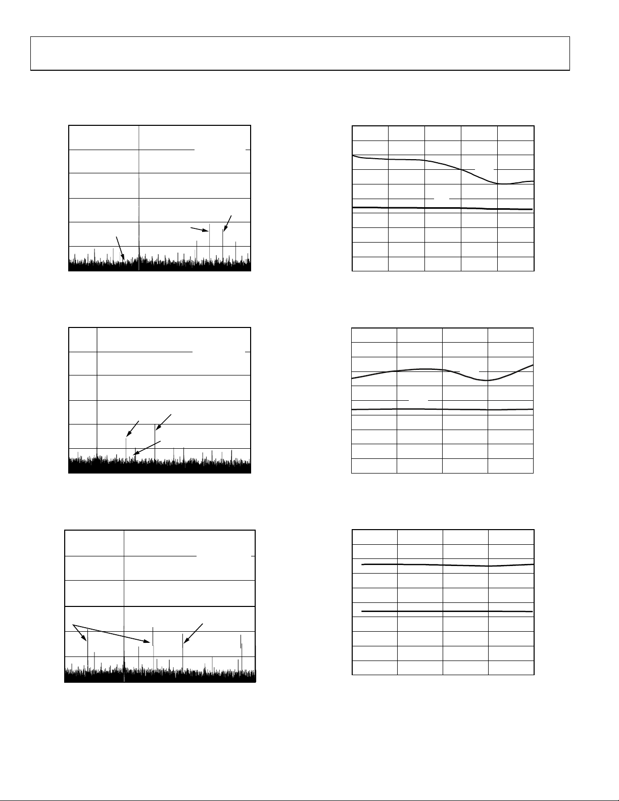
Figure 4. Single-Tone FFT of Channel A Digitizing f
While Channel B Is Digitizing f
0
–20
–40
MAGNITUDE (dBFS)
–60
–80
–100
–120
SECOND
HARMONIC
10
FREQUENCY (MHz)
THIRD HARMONIC
CROSSTALK
15 20 25 3050
Figure 5. Single-Tone FFT of Channel A Digitizing f
While Channel B Is Digitizing f
0
–20
–40
–60
CROSSTALK
–80
MAGNITUDE (dBFS)
–100
–120
10
FREQUENCY (MHz)
SECOND HARMONIC
15 20 25 3050
Figure 6. Single-Tone FFT of Channel A Digitizing f
While Channel B Is Digitizing f
SNR = 72.6dB
SINAD = 71.9dB
H2 = –81.5dBc
H3 = –86.8dBc
SFDR = 81.5dB
HARMONIC
= 10 MHz
IN
SNR = 70.5dB
SINAD = 69.4dB
H2 = –92.3dBc
H3 = –80.1dBc
SFDR = 80.1dBc
= 76 MHz
IN
SNR = 68.1dB
SINAD = 68.0dB
H2 = –83.4dBc
H3 = –83.1dBc
SFDR = 75.1dBc
= 126 MHz
IN
THIRD
= 12.5 MHz
IN
= 70 MHz
IN
= 120 MHz
IN
04446-060
04446-061
04446-062
100
95
90
85
80
75
70
SFDR/SNR (dBc)
65
60
55
50
40
45 50 55 60 65
Figure 7. AD9248-65 Single-Tone SFDR/SNR vs. FS with f
100
95
90
85
80
75
70
SFDR/SNR (dBc)
65
60
55
50
Figure 8. AD9248-40 Single-Tone SFDR/SNR vs. FS with f
100
95
90
85
80
75
70
SFDR/SNR (dBc)
65
60
55
50
0 5 10 15 20
Figure 9. AD9248-20 Single-Tone SFDR/SNR vs. FS with f
SNR
ADC SAMPLE RATE (MSPS)
SFDR
SNR
SNR
ADC SAMPLE RATE (MSPS)
ADC SAMPLE RATE (MSPS)
SFDR
35302520
SFDR
= 32.5 MHz
IN
40
= 20 MHz
IN
SNR
= 10 MHz
IN
04446-007
04446-008
04446-009
Rev. A | Page 12 of 48
AD9248
100
95
90
80
70
SFDR/SNR (dBc)
60
50
–3540–30 –25 –20 –15 –10 –5
INPUT AMPLITUDE (dBFS)
SNR
SFDR
SNR
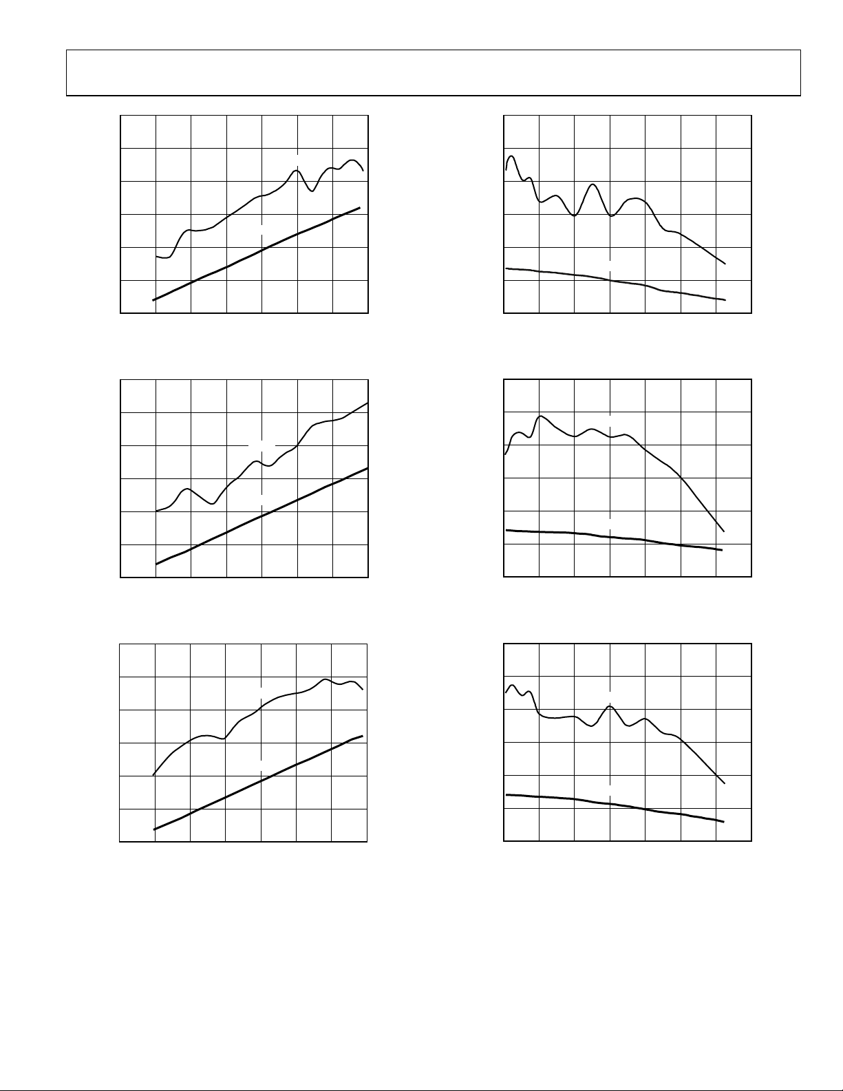
Figure 10. AD9248-65 Single-Tone SFDR/SNR vs. A
100
90
80
70
SFDR/SNR (dBc)
60
50
SNR
SFDR
SNR
0
with fIN = 32.5 MHz
IN
04446-010
90
85
80
SFDR/SNR (dBc)
75
70
06520 40 60 80 100 120
SNR
SFDR
SNR
INPUT FREQUENCY (MHz)
Figure 13. AD9248-65 Single-Tone SFDR/SNR vs. f
95
90
85
80
SFDR/SNR (dBc)
75
70
SNR
SFDR
SNR
04446-013
140
IN
–3540–30 –25 –20 –15 –10 –5
INPUT AMPLITUDE (dBFS)
Figure 11. AD9248-40 Single-Tone SFDR/SNR vs. A
100
90
SNR
SFDR
80
70
SFDR/SNR (dBc)
60
50
–3540–30 –25 –20 –15 –10 –5
INPUT AMPLITUDE (dBFS)
SNR
Figure 12. AD9248-20 Single-Tone SFDR/SNR vs. A
0
with fIN = 20 MHz
IN
0
with fIN = 10 MHz
IN
04446-011
04446-012
06520 40 60 80 100 120
INPUT FREQUENCY (MHz)
Figure 14. AD9248-40 Single-Tone SFDR/SNR vs. f
95
90
SFDR
85
80
SFDR/SNR (dBc)
75
70
06520 40 60 80 100 120
SNR
SNR
INPUT FREQUENCY (MHz)
Figure 15. AD9248-20 Single-Tone SFDR/SNR vs. f
04446-014
140
IN
04446-015
140
IN
Rev. A | Page 13 of 48
AD9248
0
–20
–40
100
SNR
95
90
85
SFDR
–60
–80
MAGNITUDE (dBFS)
–100
–120
10
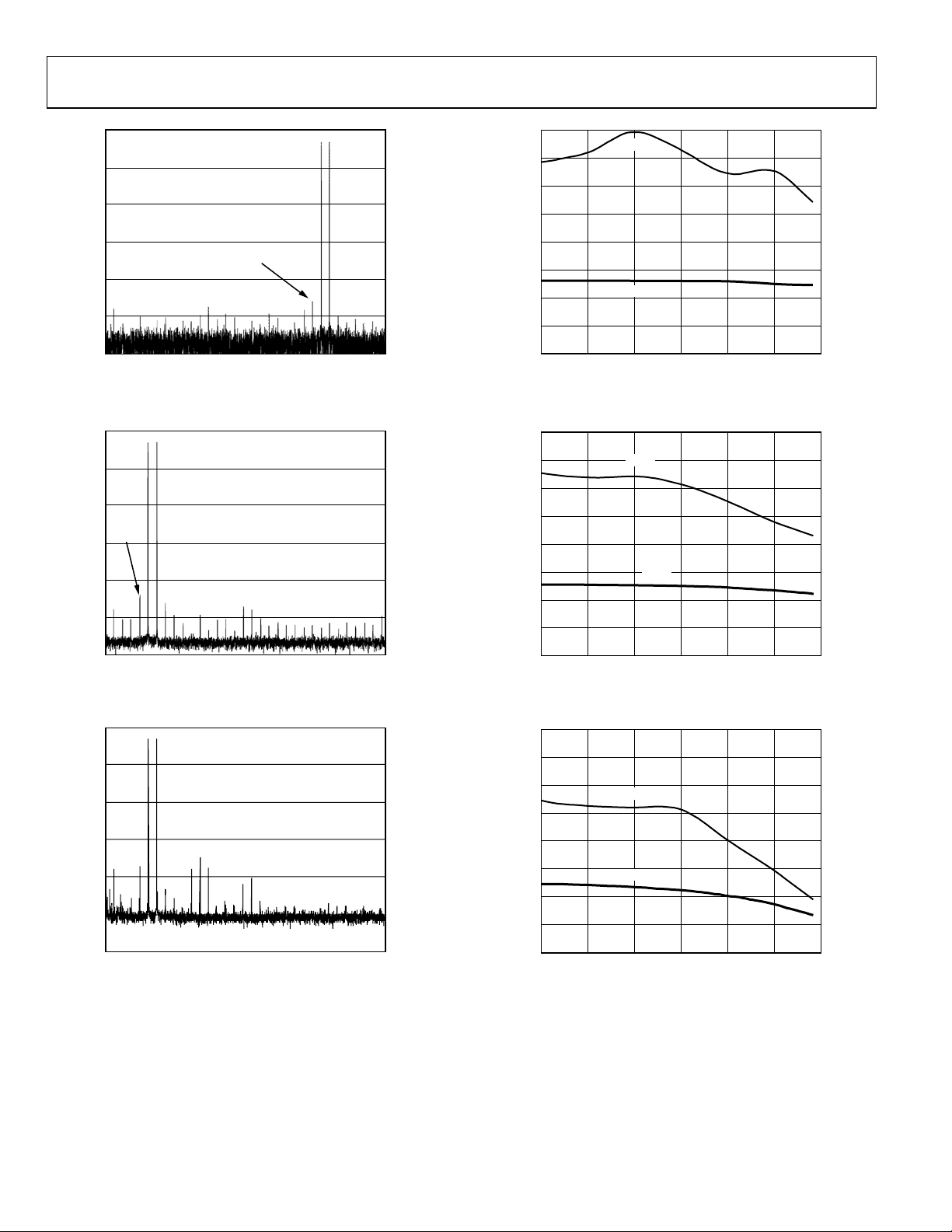
Figure 16. Dual-Tone FFT with f
0
–20
–40
IMD =
–83dBc
–60
–80
MAGNITUDE (dBFS)
–100
–120
10
Figure 17. Dual-Tone FFT with f
0
IMD = –85dBc
15 20 25 3050
FREQUENCY (MHz)
1 = 39 MHz and fIN2 = 40 MHz
IN
15 20 25 3050
FREQUENCY (MHz)
1 = 70 MHz and fIN2 = 71 MHz
IN
04446-063
04446-064
80
75
SFDR/SNR (dBFS)
65
60
–2470–21 –18 –15 –12 –9 –6
Figure 19. Dual-Tone SFDR/SNR vs. A
100
95
90
85
80
75
SFDR/SNR (dBFS)
65
60
–2470–21 –18 –15 –12 –9 –6
Figure 20. Dual-Tone SFDR/SNR vs. A
100
SNR
INPUT AMPLITUDE (dBFS)
with fIN1 = 45 MHz and fIN2 = 46 MHz
IN
SNR
SFDR
SNR
INPUT AMPLITUDE (dBFS)
with fIN1 = 70 MHz and fIN2 = 71 MHz
IN
04446-019
04446-020
–20
–40
–60
–80
MAGNITUDE (dBFS)
–100
–120
10 15 20 25 3050
Figure 18. Dual-Tone FFT with f
FREQUENCY (MHz)
1 = 200 MHz and fIN2 = 201 MHz
IN
04446-018
Rev. A | Page 14 of 48
95
90
85
80
75
SFDR/SNR (dBFS)
65
60
–2470–21 –18 –15 –12 –9 –6
SNR
SFDR
SNR
INPUT AMPLITUDE (dBFS)
Figure 21. Dual-Tone SFDR/SNR vs.
with fIN1 = 200 MHz and fIN2 = 201 MHz
A
IN
04446-021
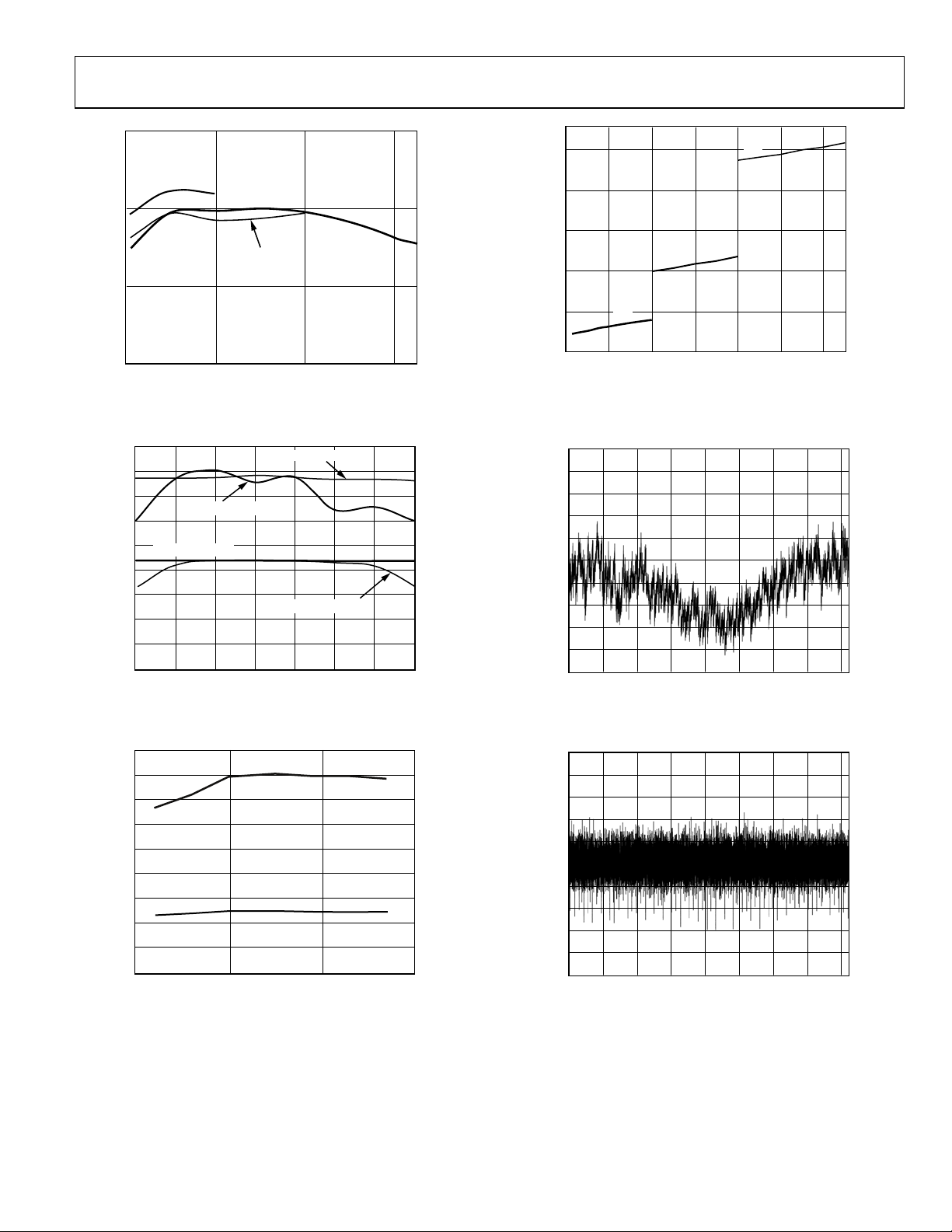
AD9248
74
12.0
600
–65
SINAD (dBc)
72
70
68
0
SINAD –20
SINAD –40
SINAD –65
20 40 60
CLOCK FREQUENCY (MHz)
11.5
11.0
ENOB
04446-022
500
400
300
AVDD POWER (mW)
200
100
0102030405060
–40
–20
SAMPLE RATE (MSPS)
Figure 25. Analog Power Consumption vs. FS
04446-025
Figure 22. SINAD vs. FS with Nyquist Input
95
90
85
80
75
70
65
SINAD/SFDR (dBc)
60
55
50
30
DCS OFF (SFDR)
DCS ON (SINAD)
35
40 45 50 55 60 65
DCS ON (SFDR)
DCS OFF (SINAD)
DUTY CYCLE (%)
04446-023
Figure 23. SINAD/SFDR vs. Clock Duty Cycle
INL (LSB)
–0.5
–1.0
–1.5
–2.0
–2.5
2.5
2.0
1.5
1.0
0.5
0
800060002000 40000 10000 12000 14000 16000
CODE
04446-026
Figure 26. AD9248-65 Typical INL
84
82
80
78
76
74
72
SINAD/SFDR (dB)
70
68
66
–50
SFDR
SINAD
0 50 100
TEMPERATURE (°C)
Figure 24. SINAD/SFDR vs. Temperature with f
= 32.5 MHz
IN
04446-024
Rev. A | Page 15 of 48
1.0
0.8
0.6
0.4
0.2
0
DNL (LSB)
–0.2
–0.4
–0.6
–0.8
–1.0
800060002000 40000 10000 12000 14000 16000
CODE
04446-027
Figure 27. AD9248-65 Typical DNL
 Loading...