

Page 1
14-Bit, 20 MSPS/40 MSPS/65 MSPS
FEATURES
Integrated dual 14-bit ADC
Single 3 V supply operation (2.7 V to 3.6 V)
SNR = 71.6 dB (to Nyquist, AD9248-65)
SFDR = 80.5 dBc (to Nyquist, AD9248-65)
Low power: 300 mW/channel at 65 MSPS
Differential input with 500 MHz, 3 dB bandwidth
Exceptional crosstalk immunity > 85 dB
Flexible analog input: 1 V p-p to 2 V p-p range
Offset binary or twos complement data format
Clock duty cycle stabilizer
Output datamux option
APPLICATIONS
Ultrasound equipment
Direct conversion or IF sampling receivers
WB-CDMA, CDMA2000,WiMAX
Battery-powered instruments
Hand-held scopemeters
Low cost digital oscilloscopes
GENERAL DESCRIPTION
The AD9248 is a dual, 3 V, 14-bit, 20 MSPS/40 MSPS/65 MSPS
analog-to-digital converter (ADC). It features dual high
performance sample-and hold amplifiers (SHAs) and an
integrated voltage reference. The AD9248 uses a multistage
differential pipelined architecture with output error correction
logic to provide 14-bit accuracy and to guarantee no missing
codes over the full operating temperature range at up to
65 MSPS data rates. The wide bandwidth, differential SHA
allows for a variety of user-selectable input ranges and offsets,
including single-ended applications. It is suitable for various
applications, including multiplexed systems that switch fullscale voltage levels in successive channels and for sampling
inputs at frequencies well beyond the Nyquist rate.
Dual single-ended clock inputs are used to control all internal
conversion cycles. A duty cycle stabilizer is available and can
compensate for wide variations in the clock duty cycle, allowing
the converter to maintain excellent performance. The digital
output data is presented in either straight binary or twos
complement format. Out-of-range signals indicate an overflow
condition, which can be used with the most significant bit to
determine low or high overflow.
Rev. A
Information furnished by Analog Devices is believed to be accurate and reliable.
However, no responsibility is assumed by Analog Devices for its use, nor for any
infringements of patents or other rights of third parties that may result from its use.
Specifications subject to change without notice. No license is granted by implication
or otherwise under any patent or patent rights of Analog Devices. Trademarks and
registered trademarks are the property of their respective owners.
Dual A/D Converter
AD9248
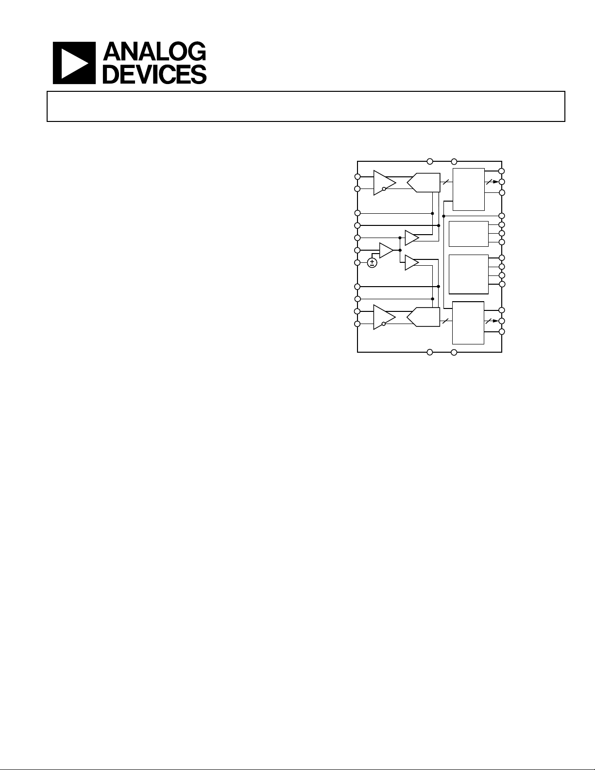
FUNCTIONAL BLOCK DIAGRAM
AVDD
AGND
VIN+_A
VIN–_A
REFT_A
REFB_A
VREF
SENSE
AGND
REFT_B
REFB_B
VIN+_B
VIN–_B
SHA
0.5V
SHA
AD9248
Fabricated on an advanced CMOS process, the AD9248 is
available in a Pb-free, space saving, 64-lead LQFP or LFCSP and
is specified over the industrial temperature range (−40°C to
+85°C).
PRODUCT HIGHLIGHTS
1. Pin-compatible with the AD9238, 12-bit 20 MSPS/
40 MSPS/65 MSPS ADC.
2. Speed grade options of 20 MSPS, 40 MSPS, and 65 MSPS
allow flexibility between power, cost, and performance to suit
an application.
3. Low power consumption: AD9248-65: 65 MSPS = 600 mW,
AD9248-40: 40 MSPS = 330 mW, and AD9248-20: 20 MSPS
= 180 mW.
4. Typical channel isolation of 85 dB @ f
5. The clock duty cycle stabilizer (AD9248-20/AD9248-40/
AD9248-65) maintains performance over a wide range of
clock duty cycles.
6. Multiplexed data output option enables single-port operation
from either Data Port A or Data Port B.
One Technology Way, P.O. Box 9106, Norwood, MA 02062-9106, U.S.A.
Tel: 781.329.4700
Fax: 781.461.3113
www.analog.com
©2005 Analog Devices, Inc. All rights reserved.
ADC
ADC
DRVDD
Figure 1.
14
OUTPUT
MUX/
BUFFERS
CLOCK
DUTY CYCLE
STABILIZER
MODE
CONTROL
OUTPUT
MUX/
BUFFERS
DRGND
14
1414
= 10 MHz.
IN
OTR_A
D13_A TO D0_A
OEB_A
MUX_SELECT
CLK_A
CLK_B
DCS
SHARED_REF
PWDN_A
PWDN_B
DFS
OTR_B
D13_B TO D0_B
OEB_B
04446-001
Page 2

AD9248
TABLE OF CONTENTS
Specifications..................................................................................... 3
Clock Circuitry ........................................................................... 22
DC Specifications ......................................................................... 3
AC Specifications.......................................................................... 5
Digital Specifications ................................................................... 6
Switching Specifications .............................................................. 7
Absolute Maximum Ratings............................................................ 8
Explanation of Test Levels........................................................... 8
ESD Caution.................................................................................. 8
Pin Configuration and Function Descriptions............................. 9
Te r mi n ol o g y .................................................................................... 11
Typical Performance Characteristics ........................................... 12
Equivalent Circuits......................................................................... 16
Theory of Operation ...................................................................... 17
Analog Input ............................................................................... 17
Clock Input and Considerations .............................................. 18
Power Dissipation and Standby Mode..................................... 19
Analog Inputs ............................................................................. 22
Reference Circuitry .................................................................... 22
Digital Control Logic................................................................. 22
Outputs ........................................................................................ 22
LQFP Evaluation Board Bill of Materials (BOM) .................. 24
LQFP Evaluation Board Schematics........................................ 25
LQFP PCB Layers....................................................................... 29
Dual ADC LFCSP PCB.................................................................. 35
Power Connector ........................................................................ 35
Analog Inputs ............................................................................. 35
Optional Operational Amplifier .............................................. 35
Clock ............................................................................................ 35
Volt a ge R e fere n ce ....................................................................... 35
Data Outputs............................................................................... 35
LFCSP Evaluation Board Bill of Materials (BOM) ................ 36
Digital Outputs ........................................................................... 19
Timing.......................................................................................... 19
Data Format ................................................................................ 20
Voltage Reference....................................................................... 20
AD9248 LQFP Evaluation Board .................................................22
REVISION HISTORY
3/05—Rev. 0 to Rev. A
Added LFCSP......................................................................Universal
Changes to Features.......................................................................... 1
Changes to Applications .................................................................. 1
Changes to General Description .................................................... 1
Changes to Product Highlights....................................................... 1
Changes to Table 6.......................................................................... 10
Changes to Terminology................................................................ 11
Changes to Figure 22...................................................................... 15
Changes to Clock Input and Considerations Section ................ 18
Changes to Timing Section ........................................................... 19
LFCSP PCB Schematics............................................................. 37
LFCSP PCB Layers..................................................................... 40
Thermal Considerations............................................................ 45
Outline Dimensions ....................................................................... 46
Ordering Guide .......................................................................... 47
Changes to Figure 33...................................................................... 19
Changes to Data Format Section.................................................. 20
Changes to Table 10 ....................................................................... 24
Changes to Figure 39...................................................................... 25
Changes to Table 13 ....................................................................... 36
Updated Outline Dimensions....................................................... 46
Changes to Ordering Guide.......................................................... 47
1/05—Revision 0: Initial Version
Rev. A | Page 2 of 48
Page 3

AD9248
SPECIFICATIONS
DC SPECIFICATIONS
AVDD = 3 V, DRVDD = 2.5 V, maximum sample rate, CLK_A = CLK_B; AIN = −0.5 dBFS differential input, 1.0 V internal reference,
to T
T
MIN
Table 1.
Parameter Temp Level Min Typ Max Min Typ Max Min Typ Max Unit
RESOLUTION Full VI 14 14 14 Bits
ACCURACY
No Missing Codes Guaranteed Full VI 14 14 14 Bits
Offset Error 25°C I ±0.2 ±1.3 ±0.2 ±1.3 ±0.2 ±1.3 % FSR
Gain Error
Differential Nonlinearity (DNL)
25°C IV ±0.6 ±1.0 ±0.6 ±1.0 ±0.65 ±1.0 LSB
Integral Nonlinearity (INL)2 Full V ±2.7 ±2.7 ±2.8 LSB
25°C IV ±2.3 ±4.5 ±2.3 ±4.5 ±2.4 ±4.5 LSB
TEMPERATURE DRIFT
Offset Error Full V ±2 ±2 ±3 ppm/°C
Gain Error1 Full V ±12 ±12 ±12 ppm/°C
INTERNAL VOLTAGE REFERENCE
Output Voltage Error (1 V Mode) Full VI ±5 ±35 ±5 ±35 ±5 ±35 mV
Load Regulation @ 1.0 mA Full V 0.8 0.8 0.8 mV
Output Voltage Error (0.5 V Mode) Full V ±2.5 ±2.5 ±2.5 mV
Load Regulation @ 0.5 mA Full V 0.1 0.1 0.1 mV
INPUT REFERRED NOISE
Input Span = 1 V 25°C V 2.1 2.1 2.1 LSB
Input Span = 2.0 V 25°C V 1.05 1.05 1.05 LSB
ANALOG INPUT
Input Span = 1.0 V Full IV 1 1 1 V p-p
Input Span = 2.0 V Full IV 2 2 2 V p-p
Input Capacitance
REFERENCE INPUT RESISTANCE Full V 7 7 7 kΩ
POWER SUPPLIES
Supply Voltages
Supply Current
PSRR Full V ±0.01 ±0.01 ±0.01 % FSR
POWER CONSUMPTION
DC Input
Sine Wave Input2 Full VI 190 217 360 400 640 700 mW
Standby Power
, DCS enabled, unless otherwise noted.
MAX
Test AD9248BST/BCP-20 AD9248BST/BCP-40 AD9248BST/BCP-65
1
3
Full IV ±0.25 ±2.2 ±0.3 ±2.4 ±0.5 ±2.5 % FSR
2
Full V ±0.65 ±0.65 ±0.7 LSB
Full V 7 7 7 pF
rms
rms
AVDD Full IV 2.7 3.0 3.6 2.7 3.0 3.6 2.7 3.0 3.6 V
DRVDD Full IV 2.25 3.0 3.6 2.25 3.0 3.6 2.25 3.0 3.6 V
IAVDD2 Full V 60 110 200 mA
IDRVDD2 Full V 5 11 16 mA
4
5
Full V 180 330 600 mW
Full V 2.0 2.0 2.0 mW
Rev. A | Page 3 of 48
Page 4

AD9248
Test AD9248BST/BCP-20 AD9248BST/BCP-40 AD9248BST/BCP-65
Parameter Temp Level Min Typ Max Min Typ Max Min Typ Max Unit
MATCHING CHARACTERISTICS
Offset Error
25°C I ±0.19 ±1.56 ±0.19 ±1.56 ±0.25 ±1.74 % FSR
(Nonshared Reference Mode)
Offset Error
25°C I ±0.19 ±1.56 ±0.19 ±1.56 ±0.25 ±1.74 % FSR
(Shared Reference Mode)
Gain Error
25°C I ±0.07 ±1.43 ±0.07 ±1.43 ±0.07 ±1.47 % FSR
(Nonshared Reference Mode)
Gain Error
25°C I ±0.01 ±0.06 ±0.01 ±0.06 ±0.01 ±0.10 % FSR
(Shared Reference Mode)
1
Gain error and gain temperature coefficient are based on the ADC only (with a fixed 1.0 V external reference).
2
Measured at maximum clock rate with a low frequency sine wave input and approximately 5 pF loading on each output bit.
3
Input capacitance refers to the effective capacitance between one differential input pin and AVSS. Refer to Figure for the equivalent analog input structure. 28
4
Measured with dc input at maximum clock rate.
5
Standby power is measured with the CLK_A and CLK_B pins inactive (that is, set to AVDD or AGND).
Rev. A | Page 4 of 48
Page 5

AD9248
AC SPECIFICATIONS
AVDD = 3 V, DRVDD = 2.5 V, maximum sample rate, CLK_A = CLK_B; AIN = −0.5 dBFS differential input, 1.0 V external reference,
to T
T
MIN
Table 2.
Parameter Temp Level Min Typ Max Min Typ Max Min Typ Max Unit
SIGNAL-TO-NOISE RATIO (SNR)
f
INPUT
25°C IV 73.1 73.7 72.8 73.4 72.3 73.1 dB
f
INPUT
25°C IV 72.4 73.1 dB
f
INPUT
25°C IV 72.3 72.9 dB
f
INPUT
25°C IV 71.2 71.6 dB
f
INPUT
SIGNAL-TO-NOISE AND DISTORTION
RATIO (SINAD)
f
INPUT
25°C IV 72.2 73.2 72.0 73.0 71.7 72.7 dB
f
INPUT
25°C IV 70.9 72.2 dB
f
INPUT
25°C IV 71.0 72.3 dB
f
INPUT
25°C IV 70.0 71.0 dB
f
INPUT
EFFECTIVE NUMBER OF BITS (ENOB)
f
INPUT
25°C IV 11.7 11.8 11.7 11.8 11.6 11.8 Bits
f
INPUT
25°C IV 11.5 11.7 Bits
f
INPUT
25°C IV 11.5 11.7 Bits
f
INPUT
25°C IV 11.3 11.5 Bits
f
INPUT
WORST HARMONIC (SECOND or THIRD)
f
INPUT
25°C IV 77.5 87.5 77.5 86.0 77.5 86.0 dBc
f
INPUT
25°C I 76.1 84.0 dBc
f
INPUT
25°C I 76.0 84.0 dBc
f
INPUT
25°C I 73.0 80.5 dBc
, DCS Enabled, unless otherwise noted.
MAX
Test AD9248BST/BCP-20 AD9248BST/BCP-40 AD9248BST/BCP-65
= 2.4 MHz Full V 73.4 73.1 72.8 dB
= 9.7 MHz Full V 72.9 dB
= 19.6 MHz Full V 72.7 dB
= 35 MHz Full V 71.5 dB
= 100 MHz 25°C V 70 69.5 69.0 dB
= 2.4 MHz Full V 73.0 72.8 72.5 dB
= 9.7 MHz Full V 72.0 dB
= 19.6 MHz Full V 72.1 dB
= 35 MHz Full V 70.9 dB
= 100 MHz 25°C V 69.5 69.0 68.5 dB
= 2.4 MHz Full V 11.8 11.8 11.8 Bits
= 9.7 MHz Full V 11.7 Bits
= 19.6 MHz Full V 11.7 Bits
= 35 MHz Full V 11.5 Bits
= 100 MHz 25°C V 11.3 11.2 11.2 Bits
= 2.4 MHz Full V 86.0 85.0 84.0 dBc
= 9.7 MHz Full V 83.0 dBc
= 19.6 MHz Full V 83.0 dBc
= 35 MHz Full V 80.0 dBc
Rev. A | Page 5 of 48
Page 6

AD9248
Test AD9248BST/BCP-20 AD9248BST/BCP-40 AD9248BST/BCP-65
Parameter Temp Level Min Typ Max Min Typ Max Min Typ Max Unit
WORST OTHER SPUR
(NONSECOND or THIRD)
f
= 2.4 MHz Full V 88.0 88.0 85.5 dBc
INPUT
25°C I 83.3 89.0 83.5 89.0 81.0 86.0 dBc
f
= 9.7 MHz Full V 87.0 dBc
INPUT
25°C I 83.1 88.0 dBc
f
= 19.6 MHz Full V 88.0 dBc
INPUT
25°C I 82.6 88.5 dBc
f
= 35 MHz Full V 85.5 dBc
INPUT
25°C I 79.8 86.0 dBc
f
= 100 MHz 25°C V 79.0 81.0 75.0 dBc
INPUT
SPURIOUS-FREE DYNAMIC RANGE (SFDR)
f
= 2.4 MHz Full V 86.0 85.0 84.0 dBc
INPUT
25°C IV 77.5 87.5 77.5 86.0 77.5 86.0 dBc
f
= 9.7 MHz Full V 83.0 dBc
INPUT
25°C I 76.1 84.0 dBc
f
= 19.6 MHz Full V 83.0 dBc
INPUT
25°C I 76.0 84.0 dBc
f
= 35 MHz Full V 80.0 dBc
INPUT
25°C I 73.0 80.5 dBc
CROSSTALK Full V −85.0 −85.0 −85.0 dB
DIGITAL SPECIFICATIONS
AVDD = 3 V, DRVDD = 2.5 V, maximum sample rate, CLK_A = CLK_B; AIN = −0.5 dBFS differential input, 1.0 V internal reference,
to T
T
MIN
Table 3.
Parameter Temp Level Min Typ Max Min Typ Max Min Typ Max Unit
LOGIC INPUTS
High Level Input Voltage Full IV 2.0 2.0 2.0 V
Low Level Input Voltage Full IV 0.8 0.8 0.8 V
High Level Input Current Full IV −10 +10 −10 +10 −10 +10 µA
Low Level Input Current Full IV −10 +10 −10 +10 −10 +10 µA
Input Capacitance Full IV 2 2 2 pF
LOGIC OUTPUTS
High Level Output Voltage Full IV
Low Level Output Voltage Full IV 0.05 0.05 0.05 V
1
Output voltage levels measured with capacitive load only on each output.
, DCS enabled, unless otherwise noted.
MAX
Test AD9248BST/BCP-20 AD9248BST-40 AD9248BST-65
1
DRVDD −
0.05
DRVDD −
0.05
DRVDD −
0.05
V
Rev. A | Page 6 of 48
Page 7
AD9248
A
SWITCHING SPECIFICATIONS
AVDD = 3 V, DRVDD = 2.5 V, maximum sample rate, CLK_A = CLK_B; AIN = −0.5 dBFS differential input, 1.0 V internal reference,
to T
T
MIN
Table 4.
Parameter Temp Level Min Typ Max Min Typ Max Min Typ Max Unit
SWITCHING PERFORMANCE
Maximum Conversion Rate Full VI 20 40 65 MSPS
Minimum Conversion Rate Full V 1 1 1 MSPS
CLK Period Full V 50.0 25.0 15.4 ns
CLK Pulse-Width High
CLK Pulse-Width Low1 Full V 15.0 8.8 6.2 ns
DATA OUTPUT PARAMETER
Output Delay2 (tPD) Full VI 2 3.5 6 2 3.5 6 2 3.5 6 ns
Pipeline Delay (Latency) Full V 7 7 7 Cycles
Aperture Delay (tA) Full V 1.0 1.0 1.0 ns
Aperture Uncertainty (tJ) Full V 0.5 0.5 0.5 ps rms
Wake-Up Time
OUT-OF-RANGE RECOVERY TIME Full V 2 2 2 Cycles
1
The AD9248-65 model has a duty cycle stabilizer circuit that, when enabled, corrects for a wide range of duty cycles (see Figure 23).
2
Output delay is measured from clock 50% transition to data 50% transition, with a 5 pF load on each output.
3
Wake-up time is dependent on the value of the decoupling capacitors; typical values shown with 0.1 µF and 10 µF capacitors on REFT and REFB.
, DCS enabled, unless otherwise noted.
MAX
1
3
Full V 15.0 8.8 6.2 ns
Full V 2.5 2.5 2.5 Ms
Test AD9248BST/BCP-20 AD9248BST/BCP-40 AD9248BST/BCP-65
N–7
N+1
N+2
N+3
N–6
N–5
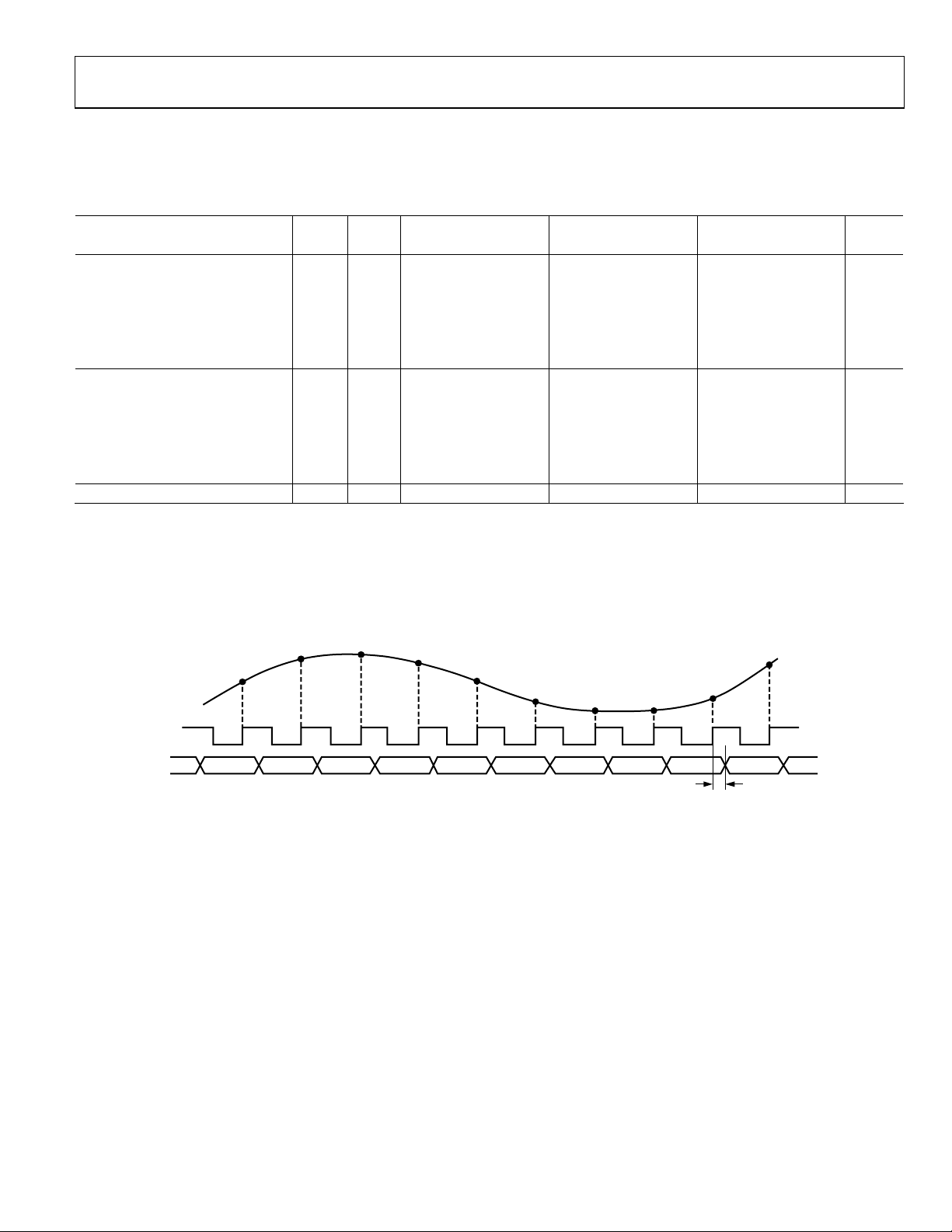
Figure 2. Timing Diagram
N–4
N+4
N–3
N+5
N–2
N+6
N–1
N+7
N
t
PD
N+8
=
MIN 2.0ns,
MAX 6.0ns
04446-002
NALOG
INPUT
CLOCK
DATA
OUT
N–9
N
N–1
N–8
Rev. A | Page 7 of 48
Page 8
AD9248
ABSOLUTE MAXIMUM RATINGS
Table 5.
Parameter Rating
Pin Name With Respect To Min Max Unit
ELECTRICAL
AVDD AGND −0.3 +3.9 V
DRVDD DRGND −0.3 +3.9 V
AGND DRGND −0.3 +0.3 V
AVDD DRVDD −3.9 +3.9 V
Digital Outputs CLK, DCS, MUX_SELECT, SHARED_REF DRGND −0.3 DRVDD + 0.3 V
OEB, DFS AGND −0.3 AVDD + 0.3 V
VINA, VINB AGND −0.3 AVDD + 0.3 V
VREF AGND −0.3 AVDD + 0.3 V
SENSE AGND −0.3 AVDD + 0.3 V
REFB, REFT AGND −0.3 AVDD + 0.3 V
PDWN AGND −0.3 AVDD + 0.3 V
ENVIRONMENTAL
Operating Temperature −45 +85 °C
Junction Temperature 150 °C
Lead Temperature (10 sec) 300 °C
Storage Temperature −65 +150 °C
1
Absolute maximum ratings are limiting values to be applied individually, and beyond which the serviceability of the circuit may be impaired. Functional operability is
not necessarily implied. Exposure to absolute maximum rating conditions for an extended period of time may affect device reliability.
2
Typical thermal impedances: 64-lead LQFP, θJA = 54°C/W; 64-lead LFCSP, θJA = 26.4°C/W with heat slug soldered to ground plane. These measurements were taken on a
4-layer board in still air, in accordance with EIA/JESD51-7.
2
1
EXPLANATION OF TEST LEVELS
I 100% production tested.
II 100% production tested at 25°C and sample tested at specified temperatures.
III Sample tested only.
IV Parameter is guaranteed by design and characterization testing.
V Parameter is a typical value only.
VI
100% production tested at 25°C; guaranteed by design and characterization testing for industrial temperature range; 100% production
tested at temperature extremes for military devices.
ESD CAUTION
ESD (electrostatic discharge) sensitive device. Electrostatic charges as high as 4000 V readily accumulate
on the human body and test equipment and can discharge without detection. Although this product features
proprietary ESD protection circuitry, permanent damage may occur on devices subjected to high energy
electrostatic discharges. Therefore, proper ESD precautions are recommended to avoid performance
degradation or loss of functionality.
Rev. A | Page 8 of 48
Page 9
AD9248
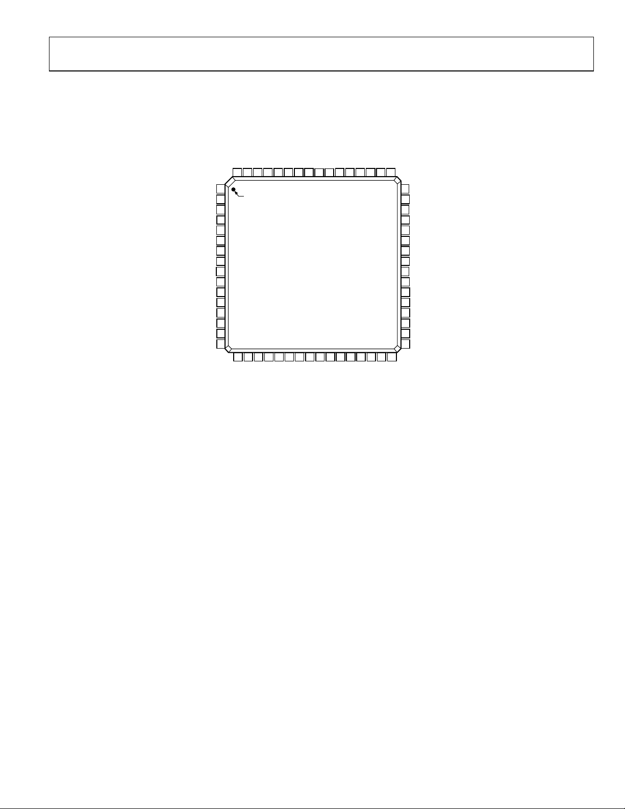
PIN CONFIGURATION AND FUNCTION DESCRIPTIONS
AVDD63CLK_A62SHARED_REF61MUX_SELECT60PDWN_A59OEB_A58OTR_A57D13_A (MSB)56D12_A55D11_A54D10_A53DRGND52DRVDD51D9_A50D8_A49D7_A
64
AGND
VIN+_A
VIN–_A
AGND
AVDD
REFT_A
REFB_A
VREF
SENSE
REFB_B
REFT_B
AVDD
AGND
VIN–_B
VIN+_B
AGND
1
PIN 1
2
3
4
5
6
7
8
9
10
11
12
13
14
15
16
17
18
19
20
21
22
AD9248
TOP VIEW
(Not to Scale)
23
24
28
29
30
48
D6_A
47
D5_A
46
D4_A
45
D3_A
44
D2_A
43
D1_A
42
D0_A (LSB)
41
DRVDD
40
DRGND
39
OTR_B
38
D13_B (MSB)
37
D12_B
36
D11_B
35
D10_B
34
D9_B
33
D8_B
AVDD
DCS
CLK_B
PDWN_B
OEB_B
D0_B (LSB)
D1_B25D2_B26D3_B27D4_B
DRVDD
DRGND
D5_B31D6_B32D7_B
DFS
Figure 3. Pin Configuration (64-Lead LQFP and 64-Lead LFCSP)
04446-003
Rev. A | Page 9 of 48
Page 10

AD9248
Table 6. Pin Function Descriptions (64-Lead LQFP and 64-Lead LFCSP)
Pin No. Mnemonic Description
1, 4, 13, 16 AGND Analog Ground.
2 VIN+_A Analog Input Pin (+) for Channel A.
3 VIN−_A Analog Input Pin (−) for Channel A.
5, 12, 17, 64 AVDD Analog Power Supply.
6 REFT_A Differential Reference (+) for Channel A.
7 REFB_A Differential Reference (−) for Channel A.
8 VREF Voltage Reference Input/Output.
9 SENSE Reference Mode Selection.
10 REFB_B Differential Reference (−) for Channel B.
11 REFT_B Differential Reference (+) for Channel B.
14 VIN−_B Analog Input Pin (−) for Channel B.
15 VIN+_B Analog Input Pin (+) for Channel B.
18 CLK_B Clock Input Pin for Channel B.
19 DCS Enable Duty Cycle Stabilizer (DCS) Mode.
20 DFS Data Output Format Select Pin (Low for Offset Binary, High for Twos Complement).
21 PDWN_B
22 OEB_B
23 to 27,
30 to 38
28, 40, 53 DRGND Digital Output Ground.
29, 41, 52 DRVDD
39 OTR_B Out-of-Range Indicator for Channel B.
42 to 51,
54 to 57
58 OTR_A Out-of-Range Indicator for Channel A.
59 OEB_A
60 PDWN_A
61 MUX_SELECT
62 SHARED_REF Shared Reference Control Pin (Low for Independent Reference Mode, High for Shared Reference Mode).
63 CLK_A Clock Input Pin for Channel A.
D0_B (LSB) to
D13_B (MSB)
D0_A (LSB) to
D13_A (MSB)
Power-Down Function Selection for Channel B.
Logic 0 enables Channel B. Logic 1 powers down Channel B (outputs static, not High-Z).
Output Enable Pin for Channel B.
Logic 0 enables Data Bus B. Logic 1 sets outputs to High-Z.
Channel B Data Output Bits.
Digital Output Driver Supply. Must be decoupled to DRGND with a minimum 0.1 µF capacitor.
Recommended decoupling is 0.1 µF capacitor in parallel with 10 µF capacitor.
Channel A Data Output Bits.
Output Enable Pin for Channel A.
Logic 0 enables Data Bus A. Logic 1 sets outputs to High-Z.
Power-Down Function Selection for Channel A
Logic 0 enables Channel A. Logic 1 powers down Channel A (outputs static, not High-Z).
Data Multiplexed Mode.
(See Data Format section for how to enable; high setting disables output data multiplexed mode.)
Rev. A | Page 10 of 48
Page 11

AD9248
TERMINOLOGY
Aperture Delay
SHA performance measured from the rising edge of the clock
input to when the input signal is held for conversion.
Aperture Jitter
The variation in aperture delay for successive samples, which is
manifested as noise on the input to the ADC.
Integral Nonlinearity (INL)
Deviation of each individual code from a line drawn from
negative full scale through positive full scale. The point used as
negative full scale occurs ½ LSB before the first code transition.
Positive full scale is defined as a level 1½ LSB beyond the last
code transition. The deviation is measured from the middle of
each particular code to the true straight line.
Differential Nonlinearity (DNL, No Missing Codes)
An ideal ADC exhibits code transitions that are exactly 1 LSB
apart. DNL is the deviation from this ideal value. Guaranteed
no missing codes to 14-bit resolution indicates that all 16,384
codes must be present over all operating ranges.
Offset Error
The major carry transition should occur for an analog value
½ LSB below VIN+ = VIN−. Offset error is defined as the
deviation of the actual transition from that point.
Gain Error
The first code transition should occur at an analog value ½ LSB
above negative full scale. The last transition should occur at an
analog value 1½ LSB below the nominal full scale. Gain error is
the deviation of the actual difference between first and last code
transitions and the ideal difference between first and last code
transitions.
Temp er at u re D ri ft
The temperature drift for zero error and gain error specifies the
maximum change from the initial (25°C) value to the value at
or T
T
MIN
MAX
.
Power Supply Rejection
The specification shows the maximum change in full scale from
the value with the supply at the minimum limit to the value
with the supply at its maximum limit.
Total Harmonic Distortion (THD)
The ratio of the rms sum of the first six harmonic components
to the rms value of the measured input signal, expressed as a
percentage or in decibels relative to the peak carrier signal (dBc).
Signal-to-Noise and Distortion (SINAD) Ratio
The ratio of the rms value of the measured input signal to the
rms sum of all other spectral components below the Nyquist
frequency, including harmonics but excluding dc. The value for
SINAD is expressed dB.
Effective Number of Bits (ENOB)
Using the following formula
ENOB = (SINAD − 1.76)/6.02
ENOB for a device for sine wave inputs at a given input
frequency can be calculated directly from its measured SINAD.
Signal-to-Noise Ratio (SNR)
The ratio of the rms value of the measured input signal to the
rms sum of all other spectral components below the Nyquist
frequency, excluding the first six harmonics and dc. The value
for SNR is expressed in dB.
Spurious-Free Dynamic Range (SFDR)
The difference in dB between the rms amplitude of the input
signal and the peak spurious signal.
Nyquist Sampling
When the frequency components of the analog input are below
the Nyquist frequency (f
/2), this is often referred to as
CLOCK
Nyquist sampling.
IF Sampling
Due to the effects of aliasing, an ADC is not limited to Nyquist
sampling. Higher sampled frequencies are aliased down into the
first Nyquist zone (DC − f
/2) on the output of the ADC.
CLOCK
The bandwidth of the sampled signal should not overlap
Nyquist zones and alias onto itself. Nyquist sampling
performance is limited by the bandwidth of the input SHA and
clock jitter (jitter adds more noise at higher input frequencies).
Two -Tone SFDR
The ratio of the rms value of either input tone to the rms value
of the peak spurious component. The peak spurious component
may or may not be an IMD product.
Out-of-Range Recovery Time
The time it takes for the ADC to reacquire the analog input
after a transient from 10% above positive full scale to 10% above
negative full scale, or from 10% below negative full scale to 10%
below positive full scale.
Crosstalk
Coupling onto one channel being driven by a (−0.5 dBFS) signal
when the adjacent interfering channel is driven by a full-scale
signal. Measurement includes all spurs resulting from both
direct coupling and mixing components.
Rev. A | Page 11 of 48
Page 12
AD9248
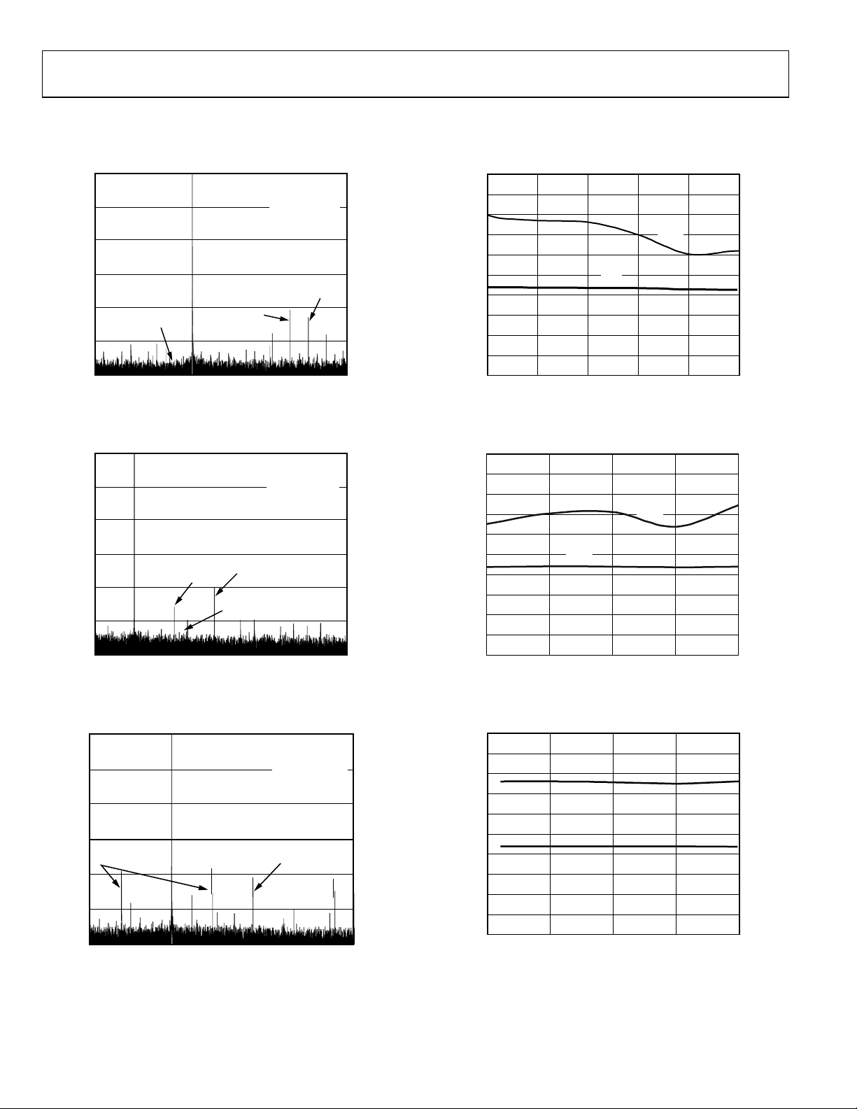
TYPICAL PERFORMANCE CHARACTERISTICS
AVDD, DRVDD = 3.0 V, T = 25°C, AIN differential drive, full scale = 2 V, unless otherwise noted.
0
–20
–40
–60
–80
MAGNITUDE (dBFS)
–100
–120
CROSSTALK
10
FREQUENCY (MHz)
SECOND
HARMONIC
15 20 25 3050
Figure 4. Single-Tone FFT of Channel A Digitizing f
While Channel B Is Digitizing f
0
–20
–40
MAGNITUDE (dBFS)
–60
–80
–100
–120
SECOND
HARMONIC
10
FREQUENCY (MHz)
THIRD HARMONIC
CROSSTALK
15 20 25 3050
Figure 5. Single-Tone FFT of Channel A Digitizing f
While Channel B Is Digitizing f
0
–20
–40
–60
CROSSTALK
–80
MAGNITUDE (dBFS)
–100
–120
10
FREQUENCY (MHz)
SECOND HARMONIC
15 20 25 3050
Figure 6. Single-Tone FFT of Channel A Digitizing f
While Channel B Is Digitizing f
SNR = 72.6dB
SINAD = 71.9dB
H2 = –81.5dBc
H3 = –86.8dBc
SFDR = 81.5dB
HARMONIC
= 10 MHz
IN
SNR = 70.5dB
SINAD = 69.4dB
H2 = –92.3dBc
H3 = –80.1dBc
SFDR = 80.1dBc
= 76 MHz
IN
SNR = 68.1dB
SINAD = 68.0dB
H2 = –83.4dBc
H3 = –83.1dBc
SFDR = 75.1dBc
= 126 MHz
IN
THIRD
= 12.5 MHz
IN
= 70 MHz
IN
= 120 MHz
IN
04446-060
04446-061
04446-062
100
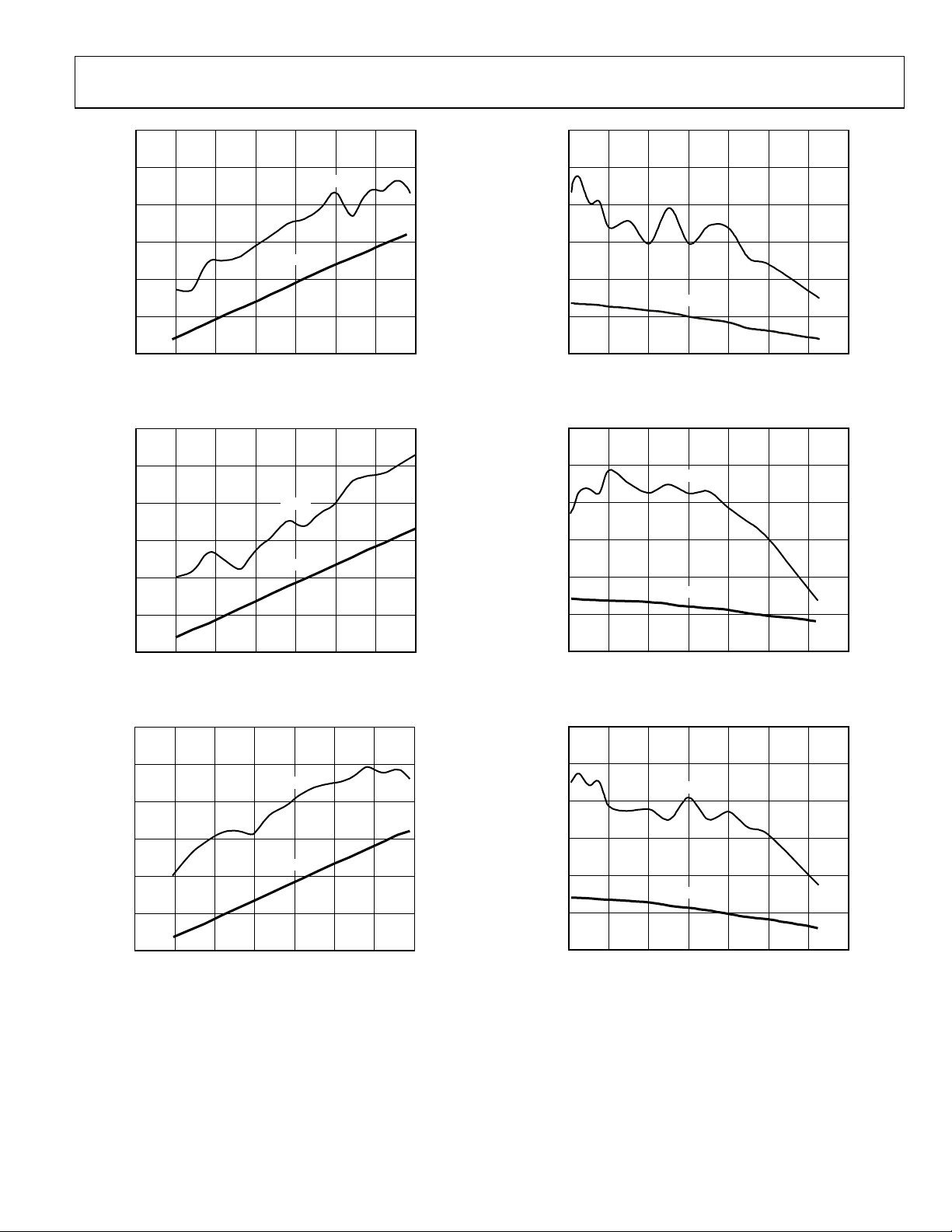
95
90
85
80
75
70
SFDR/SNR (dBc)
65
60
55
50
40
45 50 55 60 65
Figure 7. AD9248-65 Single-Tone SFDR/SNR vs. FS with f
100
95
90
85
80
75
70
SFDR/SNR (dBc)
65
60
55
50
Figure 8. AD9248-40 Single-Tone SFDR/SNR vs. FS with f
100
95
90
85
80
75
70
SFDR/SNR (dBc)
65
60
55
50
0 5 10 15 20
Figure 9. AD9248-20 Single-Tone SFDR/SNR vs. FS with f
SNR
ADC SAMPLE RATE (MSPS)
SFDR
SNR
SNR
ADC SAMPLE RATE (MSPS)
ADC SAMPLE RATE (MSPS)
SFDR
35302520
SFDR
= 32.5 MHz
IN
40
= 20 MHz
IN
SNR
= 10 MHz
IN
04446-007
04446-008
04446-009
Rev. A | Page 12 of 48
Page 13
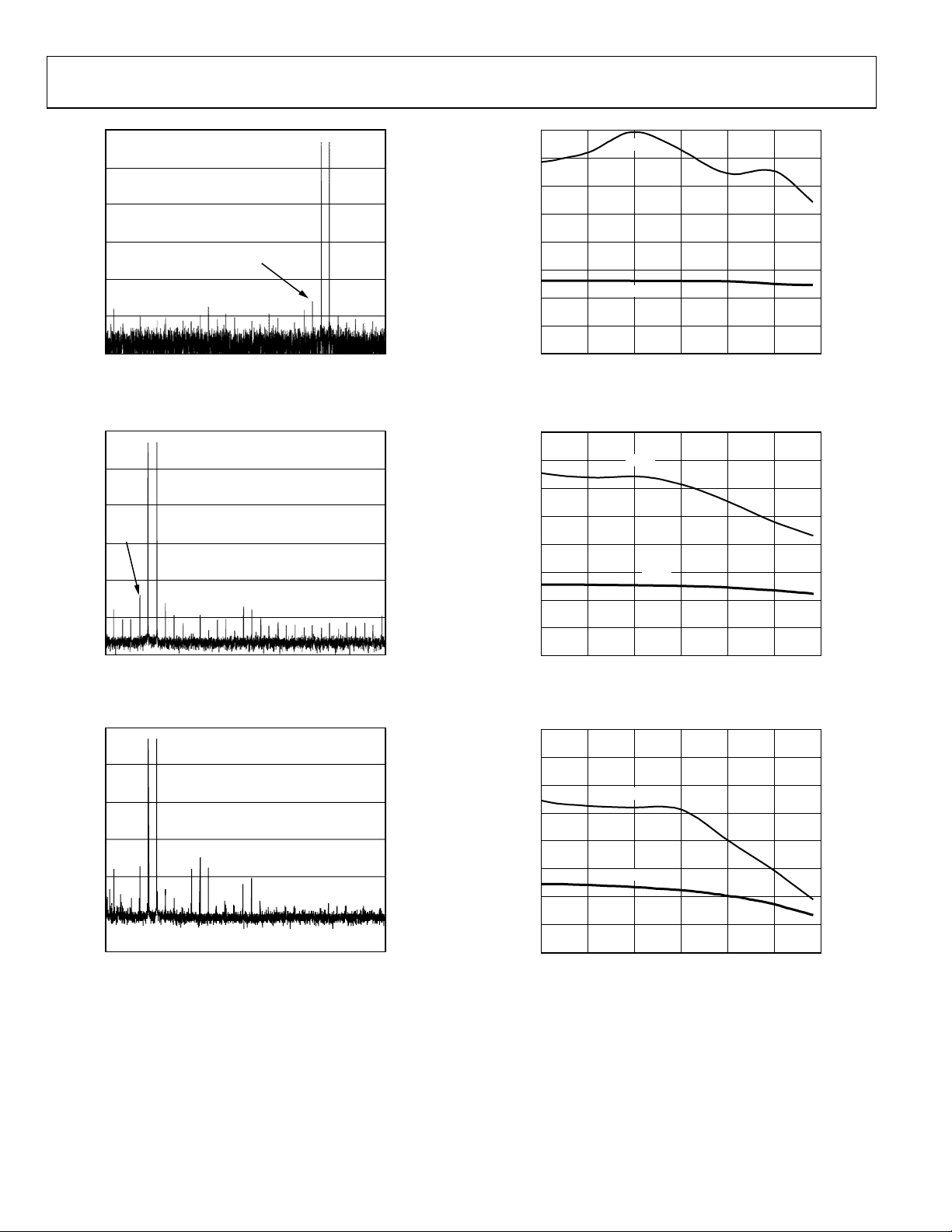
AD9248
100
95
90
80
70
SFDR/SNR (dBc)
60
50
–3540–30 –25 –20 –15 –10 –5
INPUT AMPLITUDE (dBFS)
SNR
SFDR
SNR
Figure 10. AD9248-65 Single-Tone SFDR/SNR vs. A
100
90
80
70
SFDR/SNR (dBc)
60
50
SNR
SFDR
SNR
0
with fIN = 32.5 MHz
IN
04446-010
90
85
80
SFDR/SNR (dBc)
75
70
06520 40 60 80 100 120
SNR
SFDR
SNR
INPUT FREQUENCY (MHz)
Figure 13. AD9248-65 Single-Tone SFDR/SNR vs. f
95
90
85
80
SFDR/SNR (dBc)
75
70
SNR
SFDR
SNR
04446-013
140
IN
–3540–30 –25 –20 –15 –10 –5
INPUT AMPLITUDE (dBFS)
Figure 11. AD9248-40 Single-Tone SFDR/SNR vs. A
100
90
SNR
SFDR
80
70
SFDR/SNR (dBc)
60
50
–3540–30 –25 –20 –15 –10 –5
INPUT AMPLITUDE (dBFS)
SNR
Figure 12. AD9248-20 Single-Tone SFDR/SNR vs. A
0
with fIN = 20 MHz
IN
0
with fIN = 10 MHz
IN
04446-011
04446-012
06520 40 60 80 100 120
INPUT FREQUENCY (MHz)
Figure 14. AD9248-40 Single-Tone SFDR/SNR vs. f
95
90
SFDR
85
80
SFDR/SNR (dBc)
75
70
06520 40 60 80 100 120
SNR
SNR
INPUT FREQUENCY (MHz)
Figure 15. AD9248-20 Single-Tone SFDR/SNR vs. f
04446-014
140
IN
04446-015
140
IN
Rev. A | Page 13 of 48
Page 14
AD9248
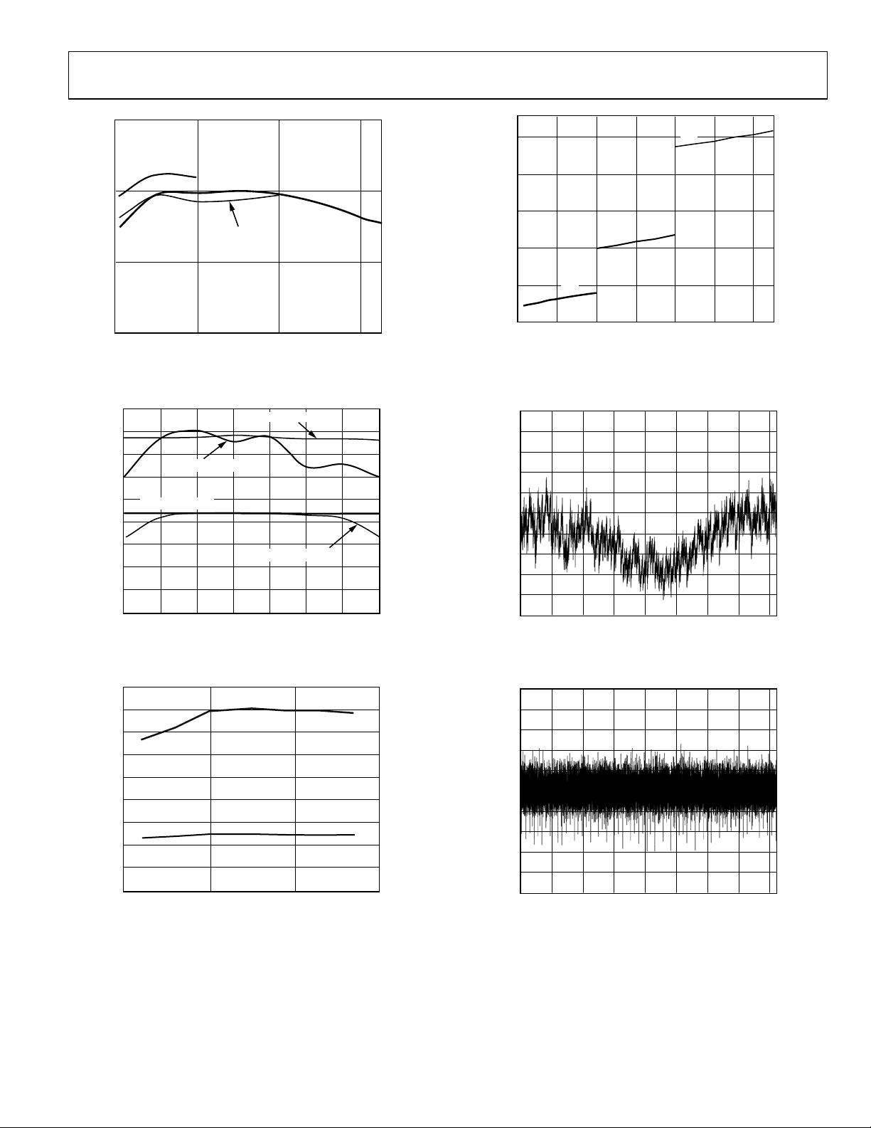
0
–20
–40
100
SNR
95
90
85
SFDR
–60
–80
MAGNITUDE (dBFS)
–100
–120
10
Figure 16. Dual-Tone FFT with f
0
–20
–40
IMD =
–83dBc
–60
–80
MAGNITUDE (dBFS)
–100
–120
10
Figure 17. Dual-Tone FFT with f
0
IMD = –85dBc
15 20 25 3050
FREQUENCY (MHz)
1 = 39 MHz and fIN2 = 40 MHz
IN
15 20 25 3050
FREQUENCY (MHz)
1 = 70 MHz and fIN2 = 71 MHz
IN
04446-063
04446-064
80
75
SFDR/SNR (dBFS)
65
60
–2470–21 –18 –15 –12 –9 –6
Figure 19. Dual-Tone SFDR/SNR vs. A
100
95
90
85
80
75
SFDR/SNR (dBFS)
65
60
–2470–21 –18 –15 –12 –9 –6
Figure 20. Dual-Tone SFDR/SNR vs. A
100
SNR
INPUT AMPLITUDE (dBFS)
with fIN1 = 45 MHz and fIN2 = 46 MHz
IN
SNR
SFDR
SNR
INPUT AMPLITUDE (dBFS)
with fIN1 = 70 MHz and fIN2 = 71 MHz
IN
04446-019
04446-020
–20
–40
–60
–80
MAGNITUDE (dBFS)
–100
–120
10 15 20 25 3050
Figure 18. Dual-Tone FFT with f
FREQUENCY (MHz)
1 = 200 MHz and fIN2 = 201 MHz
IN
04446-018
Rev. A | Page 14 of 48
95
90
85
80
75
SFDR/SNR (dBFS)
65
60
–2470–21 –18 –15 –12 –9 –6
SNR
SFDR
SNR
INPUT AMPLITUDE (dBFS)
Figure 21. Dual-Tone SFDR/SNR vs.
with fIN1 = 200 MHz and fIN2 = 201 MHz
A
IN
04446-021
Page 15
AD9248
74
12.0
600
–65
SINAD (dBc)
72
70
68
0
SINAD –20
SINAD –40
SINAD –65
20 40 60
CLOCK FREQUENCY (MHz)
11.5
11.0
ENOB
04446-022
500
400
300
AVDD POWER (mW)
200
100
0102030405060
–40
–20
SAMPLE RATE (MSPS)
Figure 25. Analog Power Consumption vs. FS
04446-025
Figure 22. SINAD vs. FS with Nyquist Input
95
90
85
80
75
70
65
SINAD/SFDR (dBc)
60
55
50
30
DCS OFF (SFDR)
DCS ON (SINAD)
35
40 45 50 55 60 65
DCS ON (SFDR)
DCS OFF (SINAD)
DUTY CYCLE (%)
04446-023
Figure 23. SINAD/SFDR vs. Clock Duty Cycle
INL (LSB)
–0.5
–1.0
–1.5
–2.0
–2.5
2.5
2.0
1.5
1.0
0.5
0
800060002000 40000 10000 12000 14000 16000
CODE
04446-026
Figure 26. AD9248-65 Typical INL
84
82
80
78
76
74
72
SINAD/SFDR (dB)
70
68
66
–50
SFDR
SINAD
0 50 100
TEMPERATURE (°C)
Figure 24. SINAD/SFDR vs. Temperature with f
= 32.5 MHz
IN
04446-024
Rev. A | Page 15 of 48
1.0
0.8
0.6
0.4
0.2
0
DNL (LSB)
–0.2
–0.4
–0.6
–0.8
–1.0
800060002000 40000 10000 12000 14000 16000
CODE
04446-027
Figure 27. AD9248-65 Typical DNL
Page 16

AD9248
V
V
EQUIVALENT CIRCUITS
AVDD
AVDD
IN+_A, VIN–_A,
IN+_B, VIN–_B
Figure 28. Equivalent Analog Input Circuit
DRVDD
04446-029
Figure 29. Equivalent Digital Output Circuit
04446-028
CLK_A, CLK_B
DCS, DFS,
MUX_SELECT,
SHARED_REF
Figure 30. Equivalent Digital Input Circuit
04446-030
Rev. A | Page 16 of 48
Page 17

AD9248
V
THEORY OF OPERATION
The AD9248 consists of two high performance ADCs that are
based on the AD9235 converter core. The dual ADC paths are
independent, except for a shared internal band gap reference
source, VREF. Each of the ADC paths consists of a proprietary
front end SHA followed by a pipelined switched-capacitor
ADC. The pipelined ADC is divided into three sections,
consisting of a 4-bit first stage, followed by eight 1.5-bit stages,
and a final 3-bit flash. Each stage provides sufficient overlap to
correct for flash errors in the preceding stages. The quantized
outputs from each stage are combined through the digital
correction logic block into a final 12-bit result. The pipelined
architecture permits the first stage to operate on a new input
sample, while the remaining stages operate on preceding
samples. Sampling occurs on the rising edge of the
respective clock.
Each stage of the pipeline, excluding the last, consists of a low
resolution flash ADC and a residual multiplier to drive the next
stage of the pipeline. The residual multiplier uses the flash ADC
output to control a switched-capacitor digital-to-analog
converter (DAC) of the same resolution. The DAC output is
subtracted from the stage’s input signal and the residual is
amplified (multiplied) to drive the next pipeline stage. The
residual multiplier stage is also called a multiplying DAC
(MDAC). One bit of redundancy is used in each one of the
stages to facilitate digital correction of flash errors. The last
stage simply consists of a flash ADC.
The input stage contains a differential SHA that can be
configured as ac- or dc-coupled in differential or single-ended
modes. The output-staging block aligns the data, carries out the
error correction, and passes the data to the output buffers. The
output buffers are powered from a separate supply, allowing
adjustment of the output voltage swing.
ANALOG INPUT
The analog input to the AD9248 is a differential, switchedcapacitor SHA that has been designed for optimum performance while processing a differential input signal. The SHA
input accepts inputs over a wide common-mode range. An
input common-mode voltage of midsupply is recommended to
maintain optimal performance.
The SHA input is a differential switched-capacitor circuit. In
Figure 31, the clock signal alternatively switches the SHA
between sample mode and hold mode. When the SHA is
switched into sample mode, the signal source must be capable
of charging the sample capacitors and settling within one-half
of a clock cycle. A small resistor in series with each input can
help reduce the peak transient current required from the output
stage of the driving source. Also, a small shunt capacitor can be
placed across the inputs to provide dynamic charging currents.
This passive network creates a low-pass filter at the ADC input;
therefore, the precise values are dependant on the application.
In IF under-sampling applications, any shunt capacitors
should be removed. In combination with the driving source
impedance, they limit the input bandwidth. For best dynamic
performance, the source impedances driving VIN+ and VIN−
should be matched such that common-mode settling errors are
symmetrical. These errors are reduced by the common-mode
rejection of the ADC.
H
T
T
H
04446-031
VIN+
IN–
T
C
PAR
T
C
PAR
Figure 31. Switched-Capacitor Input
5pF
5pF
An internal differential reference buffer creates positive and
negative reference voltages, REFT and REFB, respectively, that
define the span of the ADC core. The output common mode of
the reference buffer is set to midsupply, and the REFT and
REFB voltages and span are defined as:
REFT = ½(AV D D + V
REFB = ½(AV D D + V
Span = 2 × (REFT − REFB) = 2 × V
REF
REF
)
)
REF
The equations above show that the REFT and REFB voltages are
symmetrical about the midsupply voltage and, by definition, the
input span is twice the value of the V
voltage.
REF
The internal voltage reference can be pin-strapped to fixed
values of 0.5 V or 1.0 V or adjusted within the same range as
discussed in the Internal Reference Connection section.
Maximum SNR performance is achieved with the AD9248 set
to the largest input span of 2 V p-p. The relative SNR
degradation is 3 dB when changing from 2 V p-p mode to
1 V p-p mode.
The SHA may be driven from a source that keeps the signal
peaks within the allowable range for the selected reference
voltage. The minimum and maximum common-mode input
levels are defined as:
= V
VCM
VCM
MIN
MAX
/2
REF
= (AV D D + V
REF
)/2
Rev. A | Page 17 of 48
Page 18

AD9248
2
The minimum common-mode input level allows the AD9248 to
accommodate ground-referenced inputs. Although optimum
performance is achieved with a differential input, a singleended source may be driven into VIN+ or VIN−. In this
configuration, one input accepts the signal, while the opposite
input should be set to midscale by connecting it to an
appropriate reference. For example, a 2 V p-p signal may be
applied to VIN+, while a 1 V reference is applied to VIN−. The
AD9248 then accepts an input signal varying between 2 V and
0 V. In the single-ended configuration, distortion performance
may degrade significantly as compared to the differential case.
However, the effect is less noticeable at lower input frequencies and
in the lower speed grade models (AD9248-40 and AD9248-20).
Differential Input Configurations
As previously detailed, optimum performance is achieved while
driving the AD9248 in a differential input configuration. For
baseband applications, the AD8138 differential driver provides
excellent performance and a flexible interface to the ADC. The
output common-mode voltage of the AD8138 is easily set to
AVDD/2, and the driver can be configured in a Sallen-Key filter
topology to provide band limiting of the input signal.
At input frequencies in the second Nyquist zone and above, the
performance of most amplifiers is not adequate to achieve the
true performance of the AD9248. This is especially true in IF
under-sampling applications where frequencies in the 70 MHz
to 200 MHz range are being sampled. For these applications,
differential transformer coupling is the recommended input
configuration, as shown in Figure 32.
CLOCK INPUT AND CONSIDERATIONS
Typical high speed ADCs use both clock edges to generate a
variety of internal timing signals and, as a result, may be
sensitive to the clock duty cycle. Commonly, a 5% tolerance is
required on the clock duty cycle to maintain dynamic
performance characteristics.
The AD9248 provides separate clock inputs for each channel.
The optimum performance is achieved with the clocks operated
at the same frequency and phase. Clocking the channels
asynchronously may degrade performance significantly. In
some applications, it is desirable to skew the clock timing of
adjacent channels. The AD9248’s separate clock inputs allow for
clock timing skew (typically ±1 ns) between the channels
without significant performance degradation.
The AD9248-65 contains two clock duty cycle stabilizers, one
for each converter, that retime the nonsampling edge, providing
an internal clock with a nominal 50% duty cycle. When proper
track-and-hold times for the converter are required to maintain
high performance, maintaining a 50% duty cycle clock is
particularly important in high speed applications. It may be
difficult to maintain a tightly controlled duty cycle on the input
clock on the PCB (see Figure 23). DCS can be enabled by tying
the DCS pin high.
The duty cycle stabilizer uses a delay-locked loop to create the
nonsampling edge. As a result, any changes to the sampling
frequency require approximately 2 µs to 3 µs to allow the DLL
to acquire and settle to the new rate.
AVDD
VINA
AD9248
VINB
AGND
04446-032
V p-p
50Ω
49.9Ω
0.1µF
Figure 32. Differential Transformer Coupling
10pF
50Ω
10pF
1kΩ
1kΩ
The signal characteristics must be considered when selecting a
transformer. Most RF transformers saturate at frequencies
below a few MHz, and excessive signal power can also cause
core saturation, which leads to distortion.
Single-Ended Input Configuration
A single-ended input may provide adequate performance in
cost-sensitive applications. In this configuration, there is a
degradation in SFDR and distortion performance due to the
large input common-mode swing. However, if the source
impedances on each input are matched, there should be little
effect on SNR performance.
High speed, high resolution ADCs are sensitive to the quality of
the clock input. The degradation in SNR at a given full-scale
input frequency (f
) due only to aperture jitter (tJ) can be
INPUT
calculated as
SNR
⎡
log20
×=
⎢
()
2
⎣
In the equation, the rms aperture jitter, t
1
INPUT
, represents the root-
J
⎤
⎥
tfπ
×××
j
⎦
sum square of all jitter sources, which includes the clock input,
analog input signal, and ADC aperture jitter specification.
Under-sampling applications are particularly sensitive to jitter.
For optimal performance, especially in cases where aperture
jitter may affect the dynamic range of the AD9248, it is
important to minimize input clock jitter. The clock input
circuitry should use stable references; for example, use analog
power and ground planes to generate the valid high and low
digital levels for the AD9248 clock input. Power supplies for
clock drivers should be separated from the ADC output driver
supplies to avoid modulating the clock signal with digital noise.
Low jitter, crystal-controlled oscillators make the best clock
sources. If the clock is generated from another type of source
Rev. A | Page 18 of 48
Page 19

AD9248
(by gating, dividing, or other methods), it should be retimed by
the original clock at the last step.
discharged 0.1 µF and 10 µF decoupling capacitors on REFT
and REFB.
POWER DISSIPATION AND STANDBY MODE
The power dissipated by the AD9248 is proportional to its
sampling rates. The digital (DRVDD) power dissipation is
determined primarily by the strength of the digital drivers and
the load on each output bit. The digital drive current can be
calculated by
= V
I
DRVDD
where N is the number of bits changing, and C
load on the digital pins that changed.
The analog circuitry is optimally biased so that each speed
grade provides excellent performance while affording reduced
power consumption. Each speed grade dissipates a baseline
power at low sample rates that increases with clock frequency.
Either channel of the AD9248 can be placed into standby mode
independently by asserting the PDWN_A or PDWN_B pins.
It is recommended that the input clock(s) and analog input(s)
remain static during either independent or total standby, which
results in a typical power consumption of 1 mW for the ADC.
Note that if DCS is enabled, it is mandatory to disable the clock
of an independently powered-down channel. Otherwise,
significant distortion results on the active channel. If the clock
inputs remain active while in total standby mode, typical power
dissipation of 12 mW results.
The minimum standby power is achieved when both channels
are placed into full power-down mode (PDWN_A = PDWN_B
= HI). Under this condition, the internal references are powered
down. When either or both of the channel paths are enabled
after a power-down, the wake-up time is directly related to the
recharging of the REFT and REFB decoupling capacitors
and to the duration of the power-down. Typically, it takes
approximately 5 ms to restore full operation with fully
A
× C
DRVDD
–1
× f
CLOCK
A
1
× N
LOAD
A
2
is the average
A
3
LOAD
A
0
A single channel can be powered down for moderate power
savings. The powered-down channel shuts down internal
circuits, but both the reference buffers and shared reference
remain powered on. Because the buffer and voltage reference
remain powered on, the wake-up time is reduced to several
clock cycles.
DIGITAL OUTPUTS
The AD9248 output drivers can be configured to interface with
2.5 V or 3.3 V logic families by matching DRVDD to the digital
supply of the interfaced logic. The output drivers are sized to
provide sufficient output current to drive a wide variety of logic
families. However, large drive currents tend to cause current
glitches on the supplies that may affect converter performance.
Applications requiring the ADC to drive large capacitive loads
or large fanouts may require external buffers or latches.
The data format can be selected for either offset binary or twos
complement. See the Data Format section for more information.
TIMING
The AD9248 provides latched data outputs with a pipeline delay
of seven clock cycles. Data outputs are available one propagation delay (t
to Figure 2 for a detailed timing diagram.
The internal duty cycle stabilizer can be enabled on the AD9248
using the DCS pin. This provides a stable 50% duty cycle to
internal circuits.
The length of the output data lines and loads placed on them
should be minimized to reduce transients within the AD9248.
These transients can detract from the converter’s dynamic
performance. The lowest typical conversion rate of the AD9248
is 1 MSPS. At clock rates below 1 MSPS, dynamic performance
may degrade.
A
4
A
5
) after the rising edge of the clock signal. Refer
PD
A
A
A
6
7
8
ANALOG INPUT
ADC A
B
B
–1
0
B
–8
t
PD
Figure 33. Multiplexed Data Format Using the Channel A Output and the Same Clock Tied to CLK_A, CLK_B, and MUX_SELECT
B
1
A
B
–7
–7
B
A
–6B–6A–5
2
t
PD
B
3
B–5A
B
4
A
B
–4
–4
B
5
B
–3
–3
B
6
A
B
–2
–2
B
7
A
B
–1
–1
B
8
A
B
0
0
ANALOG INPUT
ADC B
CLK_A = CLK_B =
MUX_SELECT
A
1
D0_A TO
D11_A
04446-033
Rev. A | Page 19 of 48
Page 20

AD9248
DATA FORMAT
The AD9248 data output format can be configured for either
twos complement or offset binary. This is controlled by the data
format select pin (DFS). Connecting DFS to AGND produces
offset binary output data. Conversely, connecting DFS to AVDD
formats the output data as twos complement.
The output data from the dual ADCs can be multiplexed onto a
single 14-bit output bus. The multiplexing is accomplished by
toggling the MUX_SELECT bit, which directs channel data to
the same or opposite channel data port. When MUX_SELECT
is logic high, the Channel A data is directed to the Channel A
output bus, and the Channel B data is directed to the Channel B
output bus. When MUX_SELECT is logic low, the channel data
is reversed, that is, the Channel A data is directed to the
Channel B output bus, and the Channel B data is directed to the
Channel A output bus. By toggling the MUX_SELECT bit,
multiplexed data is available on either of the output data ports.
If the ADCs run with synchronized timing, this same clock can
be applied to the MUX_SELECT pin. Any skew between
CLK_A, CLK_B, and MUX_SELECT can degrade AC
performance. It is recommended to keep the clock skew
<100 pS. After the MUX_SELECT rising edge, either data port
has the data for its respective channel; after the falling edge, the
alternate channel’s data is placed on the bus. Typically, the other
unused bus would be disabled by setting the appropriate OEB
high to reduce power consumption and noise. Figure 33 shows
an example of multiplex mode. When multiplexing data, the
data rate is two times the sample rate. Note that both channels
must remain active in this mode and that each channel’s powerdown pin must remain low.
VOLTAGE REFERENCE
A stable and accurate 0.5 V voltage reference is built into the
AD9248. The input range can be adjusted by varying the
reference voltage applied to the AD9248, using either the
internal reference with different external resistor configurations
or an externally applied reference voltage. The input span of the
ADC tracks reference voltage changes linearly. If the ADC is
being driven differentially through a transformer, the reference
voltage can be used to bias the center tap (common-mode
voltage).
The shared reference mode allows the user to connect the
references from the dual ADCs together externally for superior
Table 7. Reference Configuration Summary
Selected Mode SENSE Voltage Resulting V
External Reference AVDD N/A 2 × External Reference
Internal Fixed Reference V
Programmable Reference 0.2 V to V
REF
REF
Internal Fixed Reference AGND to 0.2 V 1.0 2.0
0.5 1.0
0.5 × (1 + R2/R1) 2 × V
gain and offset matching performance. If the ADCs are to
function independently, the reference decoupling can be
treated independently and can provide superior isolation
between the dual channels. To enable shared reference mode,
the SHARED_REF pin must be tied high and the external
differential references must be externally shorted. (REFT_A
must be externally shorted to REFT_B, and REFB_A must be
shorted to REFB_B.)
Internal Reference Connection
A comparator within the AD9248 detects the potential at the
SENSE pin and configures the reference into four possible
states, which are summarized in Table 7. If SENSE is grounded,
the reference amplifier switch is connected to the internal
resistor divider (see Figure 34), setting VREF to 1 V.
Connecting the SENSE pin to VREF switches the reference
amplifier output to the SENSE pin, completing the loop and
providing a 0.5 V reference output. If a resistor divider is
connected, as shown in Figure 35, the switch is again set to the
SENSE pin. This puts the reference amplifier in a noninverting
mode with the VREF output defined as
= 0.5 × (1 + R2/R1)
V
REF
In all reference configurations, REFT and REFB drive the ADC
core and establish its input span. The input range of the ADC
always equals twice the voltage at the reference pin for either an
internal or an external reference.
VIN+
VIN–
VREF
10µF
0.1µF
SENSE
Figure 34. Internal Reference Configuration
(V) Resulting Differential Span (V p-p)
REF
SELECT
LOGIC
(See Figure 35)
REF
ADC
CORE
0.5V
AD9248
REFT
REFB
0.1µF
0.1µF
0.1µF
10µF
04446-034
Rev. A | Page 20 of 48
Page 21

AD9248
External Reference Operation
The use of an external reference may be necessary to
enhance the gain accuracy of the ADC or to improve thermal
drift characteristics. When multiple ADCs track one another, a
single reference (internal or external) may be necessary to
reduce gain matching errors to an acceptable level. A high
precision external reference may also be selected to provide
lower gain and offset temperature drift. Figure 36 shows the
typical drift characteristics of the internal reference in both
1 V and 0.5 V modes. When the SENSE pin is tied to AVDD,
the internal reference is disabled, allowing the use of an
external reference. An internal reference buffer loads the
external reference with an equivalent 7 kΩ load. The internal
buffer still generates the positive and negative full-scale
references, REFT and REFB, for the ADC core. The input span
is always twice the value of the reference voltage; therefore, the
external reference must be limited to a maximum of 1 V. If the
internal reference of the AD9248 is used to drive multiple
converters to improve gain matching, the loading of the
reference by the other converters must be considered. Figure 37
depicts how the internal reference voltage is affected by loading.
VIN+
10µF
10µF
SENSE
VIN–
VREF
ADC
CORE
R2
R1
SELECT
LOGIC
0.5V
REFT
REFB
0.1µF
0.1µF
0.1µF
10µF
1.2
1.0
0.8
0.6
VREF ERROR (%)
0.4
0.2
0
–40
0.05
0
–0.05
–0.10
ERROR (%)
–0.15
–0.20
–0.25
0
–30
–20 –10
0
20
10
TEMPERATURE (°C)
Figure 36. Typical VREF Drift
1V ERROR
0.5
1.0
1.5
LOAD (mA)
Figure 37. VREF Accuracy vs. Load
30
VREF = 0.5V
50 60
40
0.5V ERROR
2.0
VREF = 1V
70
2.5
04446-036
80
04446-037
3.0
AD9248
Figure 35. Programmable Reference Configuration
04446-035
Rev. A | Page 21 of 48
Page 22

AD9248
AD9248 LQFP EVALUATION BOARD
The evaluation board supports both the AD9238 and AD9248
and has five main sections: clock circuitry, inputs, reference
circuitry, digital control logic, and outputs. A description of
each section follows. Table 8 shows the jumper settings and
notes assumptions in the comment column.
Four supply connections to TB1 are necessary for the evaluation
board: the analog supply of the DUT, the on-board analog
circuitry supply, the digital driver DUT supply, and the onboard digital circuitry supply. Separate analog and digital
supplies are recommended, and on each supply 3 V is nominal.
Each supply is decoupled on-board, and each IC, including the
DUT, is decoupled locally. All grounds should be tied together.
CLOCK CIRCUITRY
The clock circuitry is designed for a low jitter sine wave source
to be ac-coupled and level shifted before driving the 74VHC04
hex inverter chips (U8 and U9) whose output provides the clock
to the part. The POT (R32 and R31) on the level shifting
circuitry allows the user to vary the duty cycle if desired. The
amplitude of the sine wave must be large enough for the trip
points of the hex inverter and within the supplies to avoid noise
from clipping. To ensure a 50% duty cycle internal to the part,
the AD9248-65 has an on-chip duty cycle stabilizer circuit that
is enabled by putting in Jumper JP11. The duty cycle stabilizer
circuitry should only be used at clock rates above 40 MSPS.
Each channel has its own clock circuitry, but normally both
clock pins are driven by a single 74VHC04, and the solder
Jumper JP24 is used to tie the clock pins together. When the
clock pins are tied together and only one 74VHC04 is being
used, the series termination resistor for the other channel must
be removed (either R54 or R55, depending on which inverter is
being used).
A data capture clock for each channel is created and sent to the
output buffers in order to be used in the data capture system if
needed. Jumper JP25 and Jumper JP26 are used to invert the
data clock, if necessary, and can be used to debug data capture
timing problems.
ANALOG INPUTS
The AD9248 achieves the best performance with a differential
input. The evaluation board has two input options for each
channel, a transformer (XFMR) and an AD8138, both of which
perform single-ended-to-differential conversions. The XFMR
allows for the best high frequency performance, and the
AD8138 is ideal for dc evaluation, low frequency inputs, and
driving an ADC differentially without loading the single-ended
signal.
The common-mode level for both input options is set to
midsupply by a resistor divider off the AVDD supply but can
also be overdriven with an external supply using the (test
points) TP12, TP13 for the AD8138s, and TP14, TP15 for the
XFMRs. For low distortion of full-scale input signals when
using an AD8138, put Jumper JP17 and Jumper JP22 in
Position B and put an external negative supply on the TP10 and
TP11 testpoints.
For best performance, use low jitter input sources and a high
performance band-pass filter after the signal source, before the
evaluation board (see Figure 38). For XFMR inputs, use solder
Jumper JP13 and Jumper JP14 for Channel A, and Jumper JP20
and Jumper JP21 for Channel B. For AD8138 inputs, use solder
Jumper JP15 and Jumper JP16 for Channel A, and Jumper JP18
and Jumper JP19 for Channel B. Remove all solder from the
jumpers not being used.
REFERENCE CIRCUITRY
The evaluation board circuitry allows the user to select a
reference mode through a series of jumpers and provides an
external reference if necessary. Please refer to Table 9 to find the
jumper settings for each reference mode. The external reference
on the board is a simple resistor divider/zener diode circuit
buffered by an AD822 (U4). The POT (R4) can be used to
change the level of the external reference to fine adjust the ADC
full scale.
DIGITAL CONTROL LOGIC
The digital control logic on the evaluation board is a series of
jumpers and pull-down resistors used as digital inputs for the
following pins on the AD9248: the power-down and output
enable bar for each channel, the duty cycle restore circuitry, the
twos complement output mode, the shared reference mode, and
the MUX_SELECT pin. Refer to Table 8 for normal operating
jumper positions.
OUTPUTS
The outputs of the AD9248 (and the data clock discussed
earlier) are buffered by 74VHC541s (U2, U3, U7, U10) to
ensure the correct load on the outputs of the DUT, as well as the
extra drive capability to the next part of the system. The
74VHC541s are latches, but on this evaluation board, they are
wired and function as buffers. Jumper JP30 can be used to tie
the data clocks together if desired. If the data clocks are tied, the
R39 or R40 resistor must be removed, depending on which
clock circuitry is being used.
Rev. A | Page 22 of 48
Page 23

AD9248
Table 8. PCB Jumpers
Normal
JP Description
Setting Comment
1 Reference Out 1 V Reference Mode
2 Reference In 1 V Reference Mode
3 Reference Out 1 V Reference Mode
4 Reference Out 1 V Reference Mode
5 Reference Out 1 V Reference Mode
6 Shared Reference Out
7 Shared Reference Out
8 PDWN B Out
9 PDWN A Out
10 Shared Reference Out
11 Duty Cycle In Duty Cycle Restore On
12 Twos Complement Out
13 Input In Using XFMR Input
14 Input In Using XFMR Input
15 Input Out Using XFMR Input
16 Input Out Using XFMR Input
17 AD8138 Supply A Using XFMR Input
18 Input Out Using XFMR Input
19 Input Out
20 Input In
21 Input In
22 AD8138 Supply A
23 Mux Select Out
24 Tie Clocks In Using One Signal for Clock
25 Data Clock A
26 Data Clock Out Using One Signal for Clock
27 Mux Select In
28 OEB_A Out
29 Mux Select Out
30 Data Clock Out
35 OEB_B Out
Table 9. Reference Jumpers
Reference Mode JP1 JP2 JP3 JP4 JP5
1 V Internal Out In Out Out Out
0.5 V Internal Out Out In Out Out
External In Out Out Out In
SINE SOURCE
LOW JITTER
SINE SOURCE
LOW JITTER
(HP8644)
BAND-PASS
FILTERS
AD9248
EVALUATION BOARD
INPUT
CIRCUITRY
Figure 38. PCB Test Setup
(HP8644)
CLOCK
CIRCUITRY
AD9248
REFERENCE MODE
SELECTION/EXTERNAL
REFERENCE/CONTROL
LOGIC
OUTPUT
BUFFERS
04446-038
Rev. A | Page 23 of 48
Page 24

AD9248
LQFP EVALUATION BOARD BILL OF MATERIALS (BOM)
Table 10.
No. Quantity Reference Designator Device Package Value
1 18 C1, C2, C11, C12, C27, C28, C33, C34, C50, C51, C73 to C76, C87 to C90 Capacitors ACASE 10 µF
2 23 C3 to C10, C29 to C31, C56, C61 to C65, C77, C79, C80, C84 to C86 Capacitors 0805 0.1 µF
3 7 C13, C15, C18, C19, C21, C23, C25 Capacitors 0603 0.001 µF
4 15 C6, C14, C16, C17, C20, C22, C24, C26, C32, C35 to C40 Capacitors 0603 0.1 µF
5 4 C41 to C44 Capacitors DCASE 22 µF
6 4 C45 to C48 Capacitors 1206 0.1 µF
7 2 C49, C53 Capacitors ACASE 6.3 V
8 2 C52, C57 Capacitors 0201 0.01 µF
9 4 C54, C55, C68, C69 Capacitors 0805
10 4 C58, C59 ,C70, C71 Capacitors 0603 DNP
11 2 C60, C72 Capacitors 0603 20 pF
12 1 D1 AD1580 SOT-23CAN 1.2 V
13 1 J1 SAM080UPM
14 14 JP1 to JP5, JP8 to JP12, JP23, JP28, JP29, JP35 JPRBLK02
15 13 JP6, JP7, JP13, JP14 to JP16, JP18 to JP21, JP24, JP27, JP30 JPRSLD02
16 4 JP17, JP22, JP25, JP26 JPRBLK03
17 4 L1 to L4 IND1210 LC1210 10 µH
18 6 R1, R2, R13, R14, R23, R27 Resistors 1206 33 Ω
19 1 R3 Resistor 1206 5.49 kΩ
20 1 R4 Resistor RV3299UP 10 kΩ
21 7 R5, R6, R38, R41, R43, R44, R51 Resistors 0805 5 kΩ
22 6 R7, R8, R19, R20, R52, R53 Resistors 1206 49.9 Ω
23 8 R9, R18, R29, R30, R47 to R50 Resistors 0805 1 kΩ
24 6 R10, R12, R15, R24, R25, R28 Resistors 1206 499 Ω
25 2 R11, R26 Resistors 1206 523 Ω
26 4 R16, R17, R21, R22 Resistors 1206 40 Ω
27 2 R31, R32 Resistors RV3299W 10 kΩ
28 4 R33 to R35, R42 Resistors 0805 500 Ω
29 2 R36, R37 Resistors 1206 10 kΩ
30 2 R39, R40 Resistors 0805 22 Ω
31 2 R54, R55 Resistors 1206 0 Ω
32 16 RP1 to RP16 Resistor Pack RCA74204 22 Ω
33 6 S1 to S6 SMA200UP
34 2 T1, T2 DIP06RCUP T1-1T
35 1 TB1 TBLK06REM
36 4 TP1, TP3, TP5, TP7 LOOPTP RED
37 4 TP2, TP4, TP6, TP8 LOOPTP BLK
38 7 TP9, TP12 to TP17 LOOPMINI WHT
39 2 TP10, TP11 LOOPMINI RED
40 1 U1 64LQFP7X7 AD9248
41 4 U2, U3, U7, U10 SOL20 74VHC541
42 1 U4 SOIC-8 AD822
43 2 U5, U6 SO8NC7 AD8138
44 2 U8, U9 TSSOP-14 74VHC04
Rev. A | Page 24 of 48
Page 25

AD9248
LQFP EVALUATION BOARD SCHEMATICS
BLK
AVDD
L2
10µH
1
AVDDIN
TB1
DUTCLKA
12
74VHC04
13
C46
C42
CLKAO
TP2
RED
TP3
L1
0.1µF
10µH
25V
22µF
DUTAVDDIN
JP24
10
AGND;7
AVDD;14
U9
11
JP25
74VHC04
RED
TP1
0Ω
R54
TP17
WHT
8
AGND;7
74VHC04
AVDD;14
U9
AGND;7
AVDD;14
U9
9
DUTAVDD
2
TB1
R1
13
A
B
2
C45
C41
33Ω
TP4
22µF
BLK
RED
TP5
0.1µF
10µHL4
25V
3
AGND
TB1
DRVDDIN
DATACLKB
DATACLKA
R2
33Ω
2
DUTDRVDD
5
TB1
1
A
B
3
C44
JP26
C48
AGND;7
TP6
0.1µF
22µF
AVDD;14
BLK
25V
U8
11
AGND
10
RED
TP7
4
TB1
AGND;7
74VHC04
DVDD
L3
10µH
6
TB1
DVDDIN
0Ω
R55
12
AVDD;14
U8
13
BLK
TP8
C47
0.1µF
C43
22µF
F25V
DUTCLKB
WHT
TP16
AGND;7
74VHC04
AVDD;14
8
U8
9
74VHC04
74VHC04
R32
10kΩ
CLKA
S6
AGND;7
C84
4
AVDD;14
74VHC04
U9
3
R42
500Ω
0.1µF
R53
49.9Ω
AGND;7
R35
AVDD;14
U8
500Ω
43
CW
AVDD
6
AGND;7
AVDD;14
U9
5
AGND;7
74VHC04
R33
500Ω
2
AVDD;14
U9
1
AVDD
CW
AGND;7
74VHC04
R31
10kΩ
C77
CLKB
S5
AVDD;14
U8
0.1µF
2
1
AGND;7
74VHC04
R34
R52
49.9Ω
AVDD;14
500Ω
U8
6
5
74VHC04
AVDD
C73
C80
C74
C79
10µF
0.1µF
10µF
0.1µF
6.3V
6.3V
04446-039
Figure 39. Evaluation Board Schematic
Rev. A | Page 25 of 48
Page 26

AD9248
JP15
VIN+_A
C59
DNP
R13
33Ω
JP14
C68
VIN–_A
SHEET 3
C60
20pF
R14
33Ω
JP16
JP13
C69
VAL
VAL
C89
C58
DNP
WHT
TP14
T1–1T
S2
XFMR INPUT A
C87
6.3V
10µF
6.3V
10µF
1
S
NC = 5
P
6
C85
C64
2
O
O
R19
49.9Ω
0.1µF
R50
1kΩ
R47
0.1µF
3
T1
4
1kΩ
R30
1kΩ
AVDD
VIN–_B
C71
DNP
R27
33Ω
JP19
C55
JP20
VAL
SHEET 3
C72
20PF
VIN+_B
C65
6.3V
R7
C63
0.1µF
R48
1kΩ
R49
1kΩ
AVDD
3
2
O
T2
O
4
49.9Ω
XFMR INPUT B
S4
0.1µF
R9
1kΩ
C90
DNP
C88
JP18
10µF
T1–1T
6.3V
10µF
WHT
TP15
1
SP
NC = 5
6
C70
R23
33Ω
JP21
C54
VAL
TP10
RED
JP17
R29
WHT
TP13
AVDD
1kΩ
AVDD
10V
C49
6.3V
04446-040
R18
WHT
TP12
AVDD
1kΩ
AVDD
R25
499Ω
RED
TP11
3
V
V
5
3
0
.
6
JP22
B
2
A
13
C62
0.1µF
C50
6.3V
10µF
1
C
R17
40Ω
R16
40Ω
2
R15
5
R12
499Ω
3
B
2
A
1
C56
0.1µF
C51
6.3V
10µF
AD8138
6
VEE
VOC
VO–
VO+
–IN
+IN
1
8
U5
R11
523Ω
AMP INPUT A
499Ω
4
VCC
3
C86
0.1µF
R10
499Ω
R20
49.9Ω
S1
R22
40Ω
AD8138
6
VEE
R28
499Ω
S3
AMP INPUT B
R21
40Ω
2
R24
4
5
VOC
VO+
VO–
–IN
+IN
8
1
U6
R26
523Ω
R8
499Ω
VCC
3
C61
0.1µF
49.9Ω
Figure 40. Evaluation Board Schematic (Continued)
Rev. A | Page 26 of 48
Page 27

AD9248
DUTAVDD
AVDD
C2
10µF
C21
C22
C19
C20
C17
C18
6.3V
0.001µF
0.1µF
0.001µF
0.1µF
0.1µF
0.001µF
JP9
JP10
DUTCLKA
646362616059585756555453525150
AVDD1
CLK_A
JP28
R6
5kΩ
R43
5kΩ
R38
5kΩ
OTRA
DA13
DA12
DA11
DA10
DA9
D10_A
DRVSS3
D9_A
DRVDD3
D12_A
D11_A
OTR_A
OEB_A
PDWN_A
SHARED_REF
MUX_SELECT
(MSB) D13_A
JP27
DA8
49
D8_A
CLKAO
DA7
DA6
D6_A
D7_A
47
JP29
DA5
D5_A
46
AVDD
DA4
D4_A
45
DA3
D3_A
JP23
DA2
44
D2_A
DUTDRVDD
C11
10µF
6.3V
C14
0.1µF
DA1
42
43
D1_A
DA0
D0_A (LSB)
OTRB
DB13
DB12
DB11
DB10
DB9
DB8
C13
0.001µF
33
34
35
36
37
38
39
40
41
C26
0.1µF
D8_B
D9_B
D10_B
D11_B
D12_B
OTR_B
DRVSS2
DRVDD2
(MSB) D13_B
U1
C25
0.001µF
AD9248
C24
C16
0.1µF
VIN+_A
VIN–_A
AVSS2
AVDD2
REFT_A
REFB_A
VREF
SENSE
REFB_B
REFT_B
AVDD3
AVSS3
VIN–_B
VIN+_B
AVSS4
AVDD4
CLK_B
DUTYEN
DFS
PDWN_B
AVSS1
C15
0.001µF
1
5
4
3
2
9
8
7
6
12
11
10
16
15
14
13
20
19
18
17
D0_B (LSB)
D1_B
D2_B
D3_B
D4_B
DRVSS1
DRVDD1
D5_B
D6_B
OEB_B
29
28
27
26
254824
23
22
21
D7_B
32
31
30
0.1µF
C23
0.001µF
AVDD
VIN–_A
VIN+_A
C52
C40
JP6
C39
0.01µF
0.1µF
AVDD
0.1µF
JP7
AGND;4
AVDD;8
+IN
576
U4 OUT
R3
–IN
5.49kΩ
AD822
CW
TP9
WHT
R4
1.2V
1
C35
0.1µF
C33
6.3V
10µF
C36
0.1µF
C38
0.1µF
C34
6.3V
10µF
C37
0.1µF
6.3V
C1
10µF
C30
0.1µF
AGND;4
AVDD;8
+IN
3
10kΩ
D1
2
1
C57
C32
OUT
U4
C29
0.1µF
VIN–_B
0.01µF
0.1µF
–IN
2
VIN+_B
JP5
AD822
DUTCLKB
C12
JP2
JP3
DB0
R44
5kΩ
R5
5kΩ
JP8
JP35
6.3V
10µF
AVDD
R51
5kΩ
R41
AVDD
5kΩ
04446-041
JP1
JP4
JP12
JP11
DUTAVDD
0.1µF
C31
R37
R36
10kΩ
10kΩ
DB7
DB6
DB5
DB4
DB3
DB2
DB1
Figure 41. Evaluation Board Schematic (Continued)
Rev. A | Page 27 of 48
Page 28

AD9248
OTRA
DA13
DA12
DA11
DA10
DA9
DA8
DA7
DA6
DA5
DA4
DA3
DA2
DA1
DA0
C75
10µF
6.3V
DATACLKA
RP9
1
RP9
2
3
RP9
RP94
RP10
RP102
RP10
3
RP10
4
RP11
RP11
2
RP11
RP11
4
RP12
RP12
2
RP12
RP12
4
C3
0.1µF
22Ω
22Ω
22Ω
22Ω
22Ω
22Ω
22Ω
22Ω
22Ω
22Ω
22Ω
22Ω
22Ω
22Ω
22Ω
22Ω
C10
0.1
0.1µF
8
7
6
5
81
7
6
5
81
7
63
5
81
7
63
5
µF
1
G1
19
G2 GND
74VHC541
A1 Y1
3
A2
4
A3
5
A4
6
A5
7
A6
8
A7
9
A8
1
G1
19
G2 GND
74VHC541
2
A1 Y1
3
A2
4
A3
5
A4
6
A5
7
A6
8
A7
9
A8
U10
0.1µF
U7
VCC
VCC
10µF
6.3V
DVDD
20
10
182
17
Y2
16
Y3
15
Y4
14
Y5
13
Y6
12
Y7
11
Y8
20
10
18
17
Y2
16
Y3
15
Y4
14
Y5
13
Y6
12
Y7
11
Y8
R40
22Ω
RP1 22Ω
RP1
2
RP1
RP14
RP2
RP22
RP2
4
RP2
RP3 81
2
RP3
RP3
4
RP3
RP4
RP42
RP4
4
RP4
22Ω
22Ω
22Ω
22Ω
22Ω
22Ω
22Ω
22Ω
22Ω
22Ω
22Ω
22Ω
22Ω
22Ω
22Ω
81
7
63
5
81
7
63
5
7
63
5
81
7
63
5
2
4
6
8
10
12
14
16
18
20
22
24
26
28
30
32
34
36
38
40
SAM080UPM
JP30
J1
HEADER UP MALE NO SHROUD
1
3
5
7
9
11
13
15
17
19
21
23
25
27
29
31
33
35
37
39
C28
C8
C9
C4
0.1µF
VCC
GND
VCC
C27
10µF
6.3V
20
10
18
17
Y2
16
Y3
15
Y4
14
Y5
13
Y6
12
Y7
11
Y8
20
10
18
17
Y2
16
Y3
15
Y4
14
Y5
13
Y6
12
Y7
11
Y8
DVDD
R39
22Ω
RP5
1
2
RP5
RP5
3
4
RP5
RP6
1
2
RP6
RP6
4
RP6
1
RP7
RP7
2
RP763
4
RP7
1
RP8
RP8
2
3
RP8
22Ω
22Ω
22Ω
22Ω
22Ω
22Ω
22Ω
22Ω
22Ω
22Ω
22Ω
22Ω
22Ω
22Ω
22Ω
RP8 22Ω
J1
HEADER UP MALE NO SHROUD
41
43
45
47
49
51
53
55
57
59
61
63
65
67
69
71
73
75
77
79
04446-042
42
8
7
6
5
8
7
63
5
8
7
5
8
7
6
54
44
46
48
50
52
54
56
58
60
62
64
66
68
70
72
74
76
78
80
SAM080UPM
OTRB
DA13
DA12
DA11
DA10
DA9
DA8
DA7
DA6
DA5
DA4
DA3
DA2
DA1
DA0
C76
10µF
6.3V
RP13
1
2
RP13
3
RP13
4
RP13
RP14
2
RP14
RP14
3
4
RP14
1
RP15
RP15
2
RP15
3
RP15
4
1
RP16
RP16
2
3
RP16
RP16
4
DATACLKB
C7
0.1µF
22Ω
22Ω
22Ω
22Ω
22Ω
22Ω
22Ω
22Ω
22Ω
22Ω
22Ω
22Ω
22Ω
22Ω
22Ω
22Ω
C6
C5
0.1µF
0.1µF
1
G1
8
7
6
5
81
7
6
5
8
7
6
5
8
7
6
5
19
2
3
4
5
6
7
8
9
1
19
2
3
4
5
6
7
8
9
U2
G2
74VHC541
A1 Y1
A2
A3
A4
A5
A6
A7
A8
G1
U3
G2 GND
74VHC541
A1 Y1
A2
A3
A4
A5
A6
A7
A8
Figure 42. Evaluation Board Schematic (Continued)
Rev. A | Page 28 of 48
Page 29

AD9248
LQFP PCB LAYERS
Figure 43. PCB Top Layer
04446-043
Rev. A | Page 29 of 48
Page 30

AD9248
Figure 44. Bottom Layer
04446-044
Rev. A | Page 30 of 48
Page 31

AD9248
Figure 45. PCB Ground Plane
04446-045
Rev. A | Page 31 of 48
Page 32

AD9248
Figure 46. PCB Split Power Plane
4446-046
Rev. A | Page 32 of 48
Page 33

AD9248
Figure 47. PCB Top Silkscreen (Note that the PCB Supports Both the AD9238 and AD9248 LQFP)
4446-049
Rev. A | Page 33 of 48
Page 34

AD9248
Figure 48. PCB Bottom Silkscreen
4446-048
Rev. A | Page 34 of 48
Page 35

AD9248
DUAL ADC LFCSP PCB
The PCB requires a low jitter clock source, analog sources, and
power supplies. The PCB interfaces directly with ADI’s standard
dual-channel data capture board (HSC-ADC-EVAL-DC),
which together with ADI’s ADC Analyzer™ software allows for
quick ADC evaluation.
POWER CONNECTOR
Power is supplied to the board via three detachable 4-lead
power strips.
Table 11. Power Connector
Terminal Comments
VCC1 3.0 V Analog supply for ADC
VDD1 3.0 V Output supply for ADC
VDL1 3.0 V Supply circuitry
VREF Optional external VREF
+5 V Optional op amp supply
−5 V Optional op amp supply
1
VCC, VDD, and VDL are the minimum required power connections.
ANALOG INPUTS
The evaluation board accepts a 2 V p-p analog input signal
centered at ground at two SMB connectors, Input A and
Input B. These signals are terminated at their respective
transformer primary side. T1 and T2 are wideband RF
transformers that provide the single-ended-to-differential
conversion, allowing the ADC to be driven differentially,
minimizing even-order harmonics. The analog signals can be
low-pass filtered at the transformer secondary to reduce high
frequency aliasing.
OPTIONAL OPERATIONAL AMPLIFIER
The PCB has been designed to accommodate an optional
AD8139 op amp that can serve as a convenient solution for
dc-coupled applications. To use the AD8139 op amp, remove
C14, R4, R5, C13, R37, and R36. Place R22, R23, R30, and R24.
1
CLOCK
The clock inputs are buffered on the board at U5 and U6. These
gates provide buffered clocks to the on-board latches, U2 and
U4, ADC input clocks, and DRA, DRB that are available at the
output Connector P3, P8. The clocks can be inverted at the
timing jumpers labeled with the respective clocks. The clock
paths also provide for various termination options. The ADC
input clocks can be set to bypass the buffers at solder bridges
P2, P9 and P10, P12. An optional clock buffer U3, U7 can also
be placed. The clock inputs can be bridged at TIEA, TIEB (R20,
R40) to allow one to clock both channels from one clock source;
however, optimal performance is obtained by driving J2 and J3.
Table 12. Jumpers
Terminal Comments
OEB A Output Enable for A Side
PDWN A Power-Down A
MUX Mux Input
SHARED REF Shared Reference Input
DR A Invert DR A
LATA Invert A Latch Clock
ENC A Invert Encode A
OEB B Output Enable for B Side
PDWN B Power-Down B
DFS Data Format Select
SHARED REF Shared Reference Input
DR B Invert DR B
LATB Invert B Latch Clock
ENC B Invert Encode B
VOLTAGE REFERENCE
The ADC SENSE pin is brought out to E41, and the internal
reference mode is selected by placing a jumper from E41 to
ground (E27). External reference mode is selected by placing a
jumper from E41 to E25 and E30 to E2. R56 and R45 allow for
programmable reference mode selection.
1
The LFCSP PCB is in development.
DATA OUTPUTS
The ADC outputs are latched on the PCB at U2, U4. The ADC
outputs have the recommended series resistors in line to limit
switching transient effects on ADC performance.
Rev. A | Page 35 of 48
Page 36

AD9248
LFCSP EVALUATION BOARD BILL OF MATERIALS (BOM)
Table 13.
No. Quantity Reference Designator Device Package Value
1 2 C1, C3 Capacitors 0201 20 pF
2 7 C2, C5, C7, C9, C10, C22, C36 Capacitors 0805 10 µF
3 44
C4, C6, C8, C11 to C15, C20, C21,
C24 to C27, C29 to C35, C39 to C61
4 6 C16 to C19, C37, C38 Capacitors TAJD 10 µF
5 2 C23, C28 Capacitors 0201 0.1 µF
6 6 J1 to J6 SMBs
7 3 P1, P4, P11 Power Connector Posts Z5.531.3425.0 Wieland
8 3 P1, P4, P11 Detachable Connectors 25.602.5453.0 Wieland
9 2 P31, P8 Connectors
10 4 R1, R2, R32, R34 Resistors 0402 36 Ω
11 6 R3, R6, R7, R8, R11, R14, R33, R42, R51, R61 Resistors 0402 50 Ω
12 4 R4, R5, R36, R37 Resistors 0402 33 Ω
13 9 R9, R10, R12, R13, R20, R35, R38, R40, R43 Resistors 0402 0 Ω
14 6 R15, R16, R18, R26, R29, R31 Resistors 0402 499 Ω
15 2 R17, R25 Resistors 0402 525 Ω
16 27
R19, R21, R27, R28, R39, R41, R44,
R46 to R49, R52, R54, R55, R57 to R60, R62 to R70
17 4 R22 to R24, R30 Resistors 0402 40 Ω
18 2 R45, R56 Resistors 0402 10 kΩ
19 1 R50 Resistor 0402 22 Ω
20 8 RZ1 to RZ6, RZ9, RZ10 Resistor Pack 220 Ω
21 2 T1, T2 Transformers AWT-1WT Mini-Circuits®
22 1 U1 AD9248 LFCSP-64
23 2 U2, U425 SN74LVTH162374 TSSOP-48
24 2 U32, U7 SN74LVC1G04 SOT-70
25 2 U5, U6 SN74VCX86 SO-14
26 2 U11, U12 AD8139 SO-8/EP
27 4 R6, R8, R33, R42 Resistors 0402 100 Ω
1
P3, P8 implemented as one 80-pin connector SAMTEC TSW-140-08-L-D-RA.
2
U3, U7 not placed.
Capacitors 0402 0.1 µF
Resistors 0402 1 kΩ
Rev. A | Page 36 of 48
Page 37

AD9248
LFCSP PCB SCHEMATICS
VD
C58
0.1µF
C36
DUT CLOCK SELECTABLE
TO BE DIRECT OR BUFFERED
VD
VD
E15
Ω
Ω
E14
E13 E12
VD
C25
Ω
0
4
3
ENCA
Y
GND
0.1µF
Ω
R42
100
R43
74LCX86
U7
VD
14
4B134A
VCC
1B1Y2A2B2Y
1A
1234567
P12
P10
R39
1kΩ
TIEA
Ω
R33
100
VD
VD
10µF
5
VCC
NC
A
SN74LVC1G04
1
2
J6
Ω
R61
50
F
µ
C56
0.1
MUX
VD
E9
E7
Ω
R64
1k
R65
VD
1kΩ
VD
E10
E17
E20
Ω
E18
R63
1k
E6
E5
R66
4123
412
3
–5V
EXT_VREFVDLVDD
+5V
EXT_VREF
VDD VDL
VD
+5V
–5V
P1
P4
VD
412
3
P11
P5P6P7
VD
H3
R46
1k
DRA
Ω
0
R10
124Y113B103A9
E4
VD
C40
0.1µF
J3
ENCODE A
C8
0.1µF
VDD
Ω
R62
1k
ENCA
Ω
1k
C45
C44
C43
C39
VD
C19
C18
C17
+ + + ++
C16
C38
+
C37
VDL
VDD
H1
R47
1k
Ω
0
8
R9
3Y
CLKLATA
MUX
Ω
0
R35
Ω
0
R38
U6
GND
P14
R44
1kΩ
E3
TO TIE CLOCKS TOGETHER
C4
D1A
R41
1kΩ
R11
50Ω
D6_A D6A48D5_A D5A47D4_A D4A46D3_A D3A45D2_A D2A44D1_A
D7_A D7A
49
D8A
D11A
D13A
1µF
.
0
1µF
.
0
1µF
.
0
0.1µF
10µF
10µF
10µF
10µF
10µF
10µF
H4
H2
D8_A
50
D9_A D9A
51
52
53
D10_A D10A
54
D11_A
55
D12_A D12A
56
D13_A
57
58
59
60
61
62
63
64
EPAD
65
AGND2VIN_A3VIN_AB4AGND1
1
C1
AMPOUTA
Ω
R4
33
F
µ
C14
0.1
Ω
R3
50
DRVDD2
DRGND2
OTR_A OTRA
OEB_A
PDWN_A
MUX_SEL
SH_REF
CLK_A
AVDD5 VD
20pF
T2
J4
43
AVDD16REFT_A
5
VD
C23
0.1µF
C24
0.1µF
Ω
R5
33
CTAPA
6
5
1
2
CTAPA
AMPINA
C31
AIN A
C55
C5
F
µ
0.1
42
7
C26
4
3
Ω
0
F
µ
0.1
D0A
41
D0_A
REFB_A
8
0.1µF
10µF
0.1µF
AMPOUTAB
R58
C9
TIEA
J5
DRVDD1
VREF
VREF
SEE
PADS TO SHORT
F
µ
10
R20
VDD
40
U1
9
C29
REFERENCES TOGETHER
Ω
1k
TIEB
Ω
0
Ω
R14
50
OTRB
39
OTR_B
DRGND1
SENSE
REFB_B11REFT_B
10
REFB_B
SENSE
C54
BELOW
C7
0.1µF
C27
REFTA
REFTB
P15
P16
VD
VD
E42
E43
Ω
R57
1k
R40
38
REFT_B
REFBA
R59
D13B
37
D13_B
12
VD
0.1µF
10µF
0.1µF
REFBB
P18
R60
Ω
1k
D12B
D12_B
AVDD2
13
C28
P17
Ω
1k
C10
BUFFERED
TO BE DIRECT OR
DUT CLOCK SELECTABLE
R6
VD
C57
0.1µF
C22
10µF
5
VCC
NC
SN74LVC1G04
1
D11B
D10B
D8B
34
36
35
33
D9_B D9B
D8_B
D11_B
D10_B
AGND214VIN_BB15VIN_B16AGND3
0.1µF
C3
20pF
AMPOUTBB
Ω
R37
33
CTAPB
6
5
4
1
2
3
CTAPB
AMPINB
F
F
µ
µ
C12
10
0.1
AIN B
Ω
ENCB
100
VD
Ω
22
4
Y
GND
A
3
2
D7_B
32
D6_B
31
D5_B
30
DRVDD
29
DRGND
28
D4_B
27
D3_B
26
D2_B
25
D1_B
24
D0_B
23
OEB_B
22
PDWN_B
21
DFS
20
DCS
19
CLK_B
18
AVDD3
17
R36
T1
J1
Ω
R8
100
R50
U3
VD
D7B
D6B
D5B
D4B
D3B
D2B
D1B
D0B
Ω
33
AMPOUTB
F
µ
C13
0.1
Ω
R7
50
E34 E16
CLKLATB
Ω
0
R12
7
62B5
2Y
GND
U5
3Y3A3B4Y4A4BVCC
8
9
1011121314
P9
P13
E36VD
P2
R52
1kΩ
C42
0.1µF
TIEB
F
µ
J2
0.1
C6
VDD
ENCB
VD
F
µ
C11
0.1
R56
VREF AND SENSE CIRCUIT
VD
Ω
R48
1k
Ω
0
41Y31B21A1
2A
R49
E35
R54
1kΩ
R51
50Ω
ENCODE B
SENSE
Ω
10k
E41
E25
VD
DRB
1kΩ
C30
R45
E37E38
R13
R70
E27
R69
R68
VD
Ω
1k
F
µ
0.1
Ω
10k
E30
VD
Ω
R55
1k
74LCX86
F
µ
C41
0.1
E31
Ω
1k
E26
VD
E33
VD
E29
E21
Ω
1k
VD
E40
E22
VD
Ω
R67
1k
E24
F
VREF
µ
C2
10
E2
EXT_VREF
MTHOLE6
MTHOLE6
04446-050
MTHOLE6
MTHOLE6
Figure 49. PCB Schematic (1 of 3)
Rev. A | Page 37 of 48
Page 38

AD9248
DRA
GND
D13P
D12P
D11P
D10P
D9Q
D8Q
D7Q
D6Q
D5Q
D4Q
D3Q
D2Q
GND
D13Q
D12Q
D11Q
D9P
D8P
D7P
D6P
D5P
D0P
D4P
D3P
D2P
D1P
DORP
DRB
D10Q
D1Q
D0Q
DORQ
DORP
D13P
16151413121110
220
RSO16ISO
OE2
D = INPUT
Q = OUTPUT
LE2
R3R1R2
23
24
2Q7
2Q8
2D7
2D8
26
25
RZ5
D12P
22
27
GND GND
37
39
37
39
P3
40
40
D9P
D8P
D11P
R4
D7P
D10P
9
R8
R7
R6
R5
8
7654312
D6P
16151413121110
220
RZ6
RSO16ISO
11131517192123252729313335
11131517192123252729313335
D5P
D4P
D3P
D2P
R5
R4
R3R1R2
4
312
13579
13579
HEADER40
246
8
101214161820222426283032343638
246
8
101214161820222426283032343638
D13Q
D11Q
D10Q
D9Q
D12Q
D1P
D0P
9
R8
R7
R6
8
765
DORQ
16151413121110
220
RZ10
R3R1R2
RSO16ISO
D8Q
9
R8
R7
R6
R5
R4
8
7
6
54312
333537
39
37
39
P8
40
28303234363840
D6Q
D3Q
D4Q
D7Q
D5Q
16151413121110
220
RZ9
RSO16ISO
R3R1R2
312
R5
R4
4
1113151719212325272931
11131517192123252729313335
D0Q
D1Q
D2Q
9
R8
R7
R6
8
765
13579
13579
HEADER40
246
8
101214161820222426283032343638
246
8
101214161820222426
C50
0.1µF
C51
0.1µF
21
28
20
2Q6
2D6
29
2Q5
2D5
12
37
1Q7
1D7
11
38
10
GND
GND
39
1Q6
1D6
9
40
1Q5
1D5
VDL
7
1Q4
VCC
VCC
1D4
43
41
42
1Q3
1D3
GND
44
GND
45
1Q2
1D2
46
1Q1
1D1
47
1
OE1
LE1
48
SN74LVCH16373A
2
3
5
6
8
4
24
2Q8
OE2
U2
D = INPUT
Q = OUTPUT
LE2
2D8
25
VDL
13
14
16
17
19
15
18
2Q3
1Q8
2Q1
2Q2
2Q4
VCC
GND
VCC
2D4
30
31
1D8
2D1
2D2
2D3
GND
36
35
33
32
34
23
26
22
2Q7
2D7
27
GND GND
21
28
20
2Q6
2D6
29
2Q5
2D5
VDL
13
14
16
17
19
15
18
2Q1
2Q2
2Q3
2Q4
VCC
VCC
2D4
30
31
1Q8
GND
GND
1D8
2D1
2D2
2D3
36
35
33
32
34
12
37
1Q7
1D7
11
38
10
GND
GND
39
9
1Q6
1D6
40
1Q5
1D5
VDL
2
3
5
6
8
4
7
1Q4
VCC
VCC
1D4
43
41
42
1Q3
1D3
GND
GND
44
45
1Q2
1D2
46
1Q1
1D1
47
1
OE1
LE1
48
U4
SN74LVCH16373A
C52
0.1µF
C53
0.1µF
C46
0.1µF
C47
0.1µF
C48
0.1µF
C49
0.1µF
CLKLATA
16151413121110
220
RZ3
RSO16ISO
OTRA
D13A
R3R1R2
D12A
VDL
9
220
R8
R7
R6
R5
R4
8
7
6
D11A
54312
D9A
D10A
RZ4
D8A
D7A
VDL
16151413121110
R4
R3R1R2
RSO16ISO
D3A
D6A
D4A
D5A
CLKLATA
9
R8
R7
R6
R5
8
7654312
D2A
D0A
D1A
CLKLATB
16151413121110
220
RZ1
RSO16ISO
D13B
OTRB
VDL
9
220
R8
R7
R6
R5
R4
R3R1R2
8
7
654
312
D12B
D11B
D10B
D9B
RZ2
D8B
D7B
VDL
16151413121110
R4
R3R1R2
4
312
RSO16ISO
D5B
D6B
D4B
D3B
CLKLATB
9
R8
R7
R6
R5
8
765
D0B
D2B
D1B
VDL
04446-051
Figure 50. PCB Schematic (2 of 3)
Rev. A | Page 38 of 48
Page 39

AD9248
C59
R18
C21
R19
1kΩ
VD
R16
499Ω
AMPINA
OP AMP INPUT OFF PIN 1 OF TRANSFORMER
R17
525Ω
R21
9
C60
499Ω
0.1µF
1kΩ
1
–IN
EPAD
+IN
8
C32
0.1µF
+5V
R22
40Ω
4
36
2
V+
VOCM
U11
+OUT
AD8139
V–
–OUT
NC
5
7
C33
0.1µF
–5V
R23
40Ω
AMPOUTAB AMPOUTA
AMPINB
R26
499Ω
C20
R28
1kΩ
VD
R25
525Ω
9
R29
499Ω
Figure 51. PCB Schematic (3 of 3)
R15
C15
R27
C34
C61
499Ω
0.1µF
1kΩ
1
–IN
EPAD
+IN
8
0.1µF
R31
499Ω
C35
0.1µF
+5V
R30
40Ω
4
36
2
V+
VOCM
U12
+OUT
AMPOUTBB
AD8139
V–
–OUT
NC
5
7
–5V
R24
40Ω
AMPOUTB
04446-052
Rev. A | Page 39 of 48
Page 40

AD9248
LFCSP PCB LAYERS
Figure 52. PCB Top-Side Silkscreen
04446-053
Rev. A | Page 40 of 48
Page 41

AD9248
Figure 53. PCB Top-Side Copper Routing
04446-054
Rev. A | Page 41 of 48
Page 42

AD9248
Figure 54. PCB Ground Layer
04446-055
Rev. A | Page 42 of 48
Page 43

AD9248
Figure 55. PCB Split Power Plane
04446-056
Rev. A | Page 43 of 48
Page 44

AD9248
Figure 56. PCB Bottom-Side Copper Routing
04446-057
Rev. A | Page 44 of 48
Page 45

AD9248
Figure 57. PCB Bottom-Side Silkscreen
THERMAL CONSIDERATIONS
The AD9248 LFCSP has an integrated heat slug
that improves the thermal and electrical properties of the
package when locally attached to a ground plane at the PCB.
A thermal (filled) via array to a ground plane beneath the
part provides a path for heat to escape the package, lowering
junction temperature. Improved electrical performance
also results from the reduction in package parasitics due to
proximity of the ground plane. Recommended array is 0.3 mm
vias on 1.2 mm pitch. θ
configuration. Soldering the slug to the PCB is a requirement
for this package.
= 26.4°C/W with this recommended
JA
04446-058
04446-059
Figure 58. Thermal Via Array
Rev. A | Page 45 of 48
Page 46

AD9248
Q
OUTLINE DIMENSIONS
1.45
1.40
1.35
0.15
SEATING
0.05
PLANE
VIEW A
ROTATED 90° CCW
PIN 1
INDICATOR
9.00
BSC SQ
0.75
0.60
0.45
0.20
0.09
7°
3.5°
0°
0.10 MAX
COPLANARITY
COMPLIANT TO JEDEC STANDARDS MS-026-BBD
1.60
MAX
VIEW A
1
16
17
PIN 1
0.40
BSC
LEAD PITCH
Figure 59. 64-Lead Low Profile Quad Flat Package [LQFP]
(ST-64-1)
Dimensions shown in millimeters
49
48
0.60 MAX
0.60 MAX
9.00
BSC SQ
TOP VIEW
(PINS DOWN)
0.23
0.18
0.13
0.30
0.25
0.18
4964
48
7.00
BSC S
33
32
PIN 1
64
1
INDICATOR
1.00
0.85
0.80
12° MAX
SEATING
PLANE
TOP
VIEW
0.80 MAX
0.65 TYP
0.50 BSC
*
COMPLIANT TO JEDEC STANDARDS MO-220-VMMD
EXCEPT FOR EXPOSED PAD DIMENSION
8.75
BSC SQ
0.20 REF
0.45
0.40
0.35
0.05 MAX
0.02 NOM
33
32
Figure 60. 64-Lead Lead Frame Chip Scale Package [LFCSP_VQ]
9 mm × 9 mm Body, Very Thin Quad
(CP-64-1)
Dimensions shown in millimeters
EXPOSED PAD
(BOTTOM VIEW)
7.50
REF
*
4.85
4.70 SQ
4.55
16
17
Rev. A | Page 46 of 48
Page 47

AD9248
ORDERING GUIDE
Model Temperature Range Package Description Package Option
AD9248BSTZ-20
AD9248BSTZ-401 –40°C to +85°C 64-Lead Low Profile Quad Flat Package (LQFP) ST-64-1
AD9248BSTZ-651 –40°C to +85°C 64-Lead Low Profile Quad Flat Package (LQFP) ST-64-1
AD9248BSTZRL-201 –40°C to +85°C 64-Lead Low Profile Quad Flat Package (LQFP) ST-64-1
AD9248BSTZRL-401 –40°C to +85°C 64-Lead Low Profile Quad Flat Package (LQFP) ST-64-1
AD9248BSTZRL-651 –40°C to +85°C 64-Lead Low Profile Quad Flat Package (LQFP) ST-64-1
AD9248BCPZ-201 –40°C to +85°C 64-Lead Lead Frame Chip Scale Package (LFCSP_VQ) CP-64-1
AD9248BCPZ-401 –40°C to +85°C 64-Lead Lead Frame Chip Scale Package (LFCSP_VQ) CP-64-1
AD9248BCPZ-651 –40°C to +85°C 64-Lead Lead Frame Chip Scale Package (LFCSP_VQ) CP-64-1
AD9248BCPZRL-201 –40°C to +85°C 64-Lead Lead Frame Chip Scale Package (LFCSP_VQ) CP-64-1
AD9248BCPZRL-401 –40°C to +85°C 64-Lead Lead Frame Chip Scale Package (LFCSP_VQ) CP-64-1
AD9248BCPZRL-651 –40°C to +85°C 64-Lead Lead Frame Chip Scale Package (LFCSP_VQ) CP-64-1
AD9248BSTZ-65EB1 Evaluation Board with AD9248BSTZ-65
AD9248BCPZ-65EB1 Evaluation Board with AD9248BCPZ-65
1
Z = Pb-free part.
1
–40°C to +85°C 64-Lead Low Profile Quad Flat Package (LQFP) ST-64-1
Rev. A | Page 47 of 48
Page 48

AD9248
NOTES
©2005 Analog Devices, Inc. All rights reserved. Trademarks and
registered trademarks are the property of their respective owners.
D04446–0–3/05(A)
Rev. A | Page 48 of 48
 Loading...