PRELIMINAR Y TECHNICAL D A T A
a
14-Bit, 40/65 MSPS
Monolithic A/D Converter
Preliminary Technical Data
FEATURES
14-Bit, 65MSPS ADC
Low Power:
- 590mW at 65MSPS with Fin to Nyquist
- 340mW at 40MSPS with Fin to Nyquist
On-Chip Reference and Sample/Hold
750MHz Analog Input Bandwidth
SNR = 74dB up to Nyquist
SFDR = 83dB up to Nyquist
Differential Non Linearity Error = ±0.6LSB
Guaranteed No Missing Codes Over Full Temp range
1V to 2V p-p Differential Full Scale Analog Input Range
Single +5.0V Analog Supply, 3/5V Driver Supply
Out-of-Range Indicator
Straight Binary or Two’s Complement Output Data
48-Lead LQFP Package
APPLICATIONS
Communications Subsystems (Microcell, Picocell)
Medical and High End Imaging Equipment
Ultrasound Equipment
PRODUCT DESCRIPTION
The AD9244 is a monolithic, single 5V supply, 14-bit,
65MSPS Analog to Digital Converter with an on-chip,
high performance sample and hold amplifier and voltage
reference. The AD9244 uses a multi-stage differential
pipelined architecture with output error correction logic to
provide 14-bit accuracy at 65MSPS data rates and
guarantees no missing codes over the full operating
temperature range.
The AD9244 has an on-board, programmable voltage
reference. An external reference can also be chosen to suit
the DC accuracy and temperature drift requirements of the
application.
A differential clock input is used to control all internal
conversion cycles. The digital output data can be presented in straight binary or in two’s complement format.
An out of range (OTR) signal indicates an overflow condition, which can be used with the most significant bit to
determine low or high overflow.
Fabricated on an advanced CMOS process, the AD9244 is
available in a 48 pin surface mount plastic package (48
LQFP) and is specified for operation over the industrial
temperature range of (-40°C to +85°C).
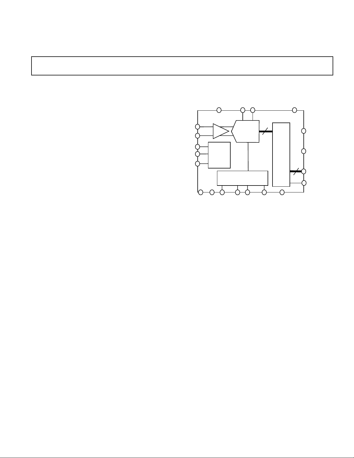
VIN+
VIN-
CLK+
CLK-
DUTY
AD9244
FUNCTIONAL BLOCK DIAGRAM
AVDD DRVDD
AD9244
SHA
TIMING
AGND DRGNDVREF REF
PRODUCT HIGHLIGHTS
Low Power—The AD9244 at 590mW consumes a fraction
of the power of presently available in existing, high speed
monolithic solutions.
On-Board Sample-and-Hold (SHA)—The versatile SHA
input can be configured for either single-ended or differential inputs.
Out of Range (OTR)—The OTR output bit indicates when
the input signal is beyond the AD9244’s input range.
Single Supply—The AD9244 uses a single +5V power supply simplifying system power supply design. It also features
a separate digital output driver supply line to accommodate
3V and 5V logic families.
IF Sampling—The AD9244 delivers outstanding performance at input frequencies beyond the first Nyquist zone.
Sampling at 65MSPS, with an input frequency of 100MHz,
the AD9244 delivers 70dB SNR and SFDR of 82dB.
REFT REFB
REFERENCE
VRCML
EIGHT
STAGE
PIPELINE
ADC
SENSE
14
REF
GND
OUTPUT REGISTER
DFS
OTR
DB13-DB0
14
OEB
REV. PrD 01/22/02
Information furnished by Analog Devices is believed to be accurate and
reliable. However, no responsibility is assumed by Analog Devices for its
use, nor for any infringements of patents or other rights of third parties
which may result from its use. No license is granted by implication or
otherwise under any patent or patent rights of Analog Devices.
One Technology Way, P.O. Box 9106, Norwood, MA 020629106, U.S.A.
Tel: 781/329-4700 www.analog.com
Fax: 781/326-8703 © Analog Devices, Inc., 2002

PRELIMINARY TECHNICAL DAT A
AD9244–SPECIFICATIONS
DC SPECIFICATIONS
INPUTS, DIFFERENTIAL CLOCK INPUTS, EXTERNAL REFERENCE, T
(AVDD = +5 V , CLKVDD=3V , DRVDD = +3.0 V , f
to T
unless otherwise noted)
MIN
MAX
= 65 MSPS (-65) or 40MSPS (-40), INPUT RANGE = 2V p-p, DIFFERENTIAL ANALOG
SAMPLE
Test AD9244BST-65 AD9244BST-40
Parameter Temp Level Mi n T y p Ma x Min Typ Ma x Units
RESOLUTION Full VI 14 14 bits
DC ACCURACY
No Missing Codes Guaranteed Full VI 14 14 bits
Offset Error Full VI %FSR
Gain Error
Differential Nonlinearity (DNL)
Integral Nonlinearity (INL)
1
2
Full VI %FSR
2
Full IV L SB
+25°C I ±0.6 ±0.6 LS B
Full IV L SB
+25°C I ±1.9 ±1.3 LS B
TEMPERATURE DRIFT
Offset Error Full V ppm/°C
Gain Error
1
Full V ppm/°C
INTERNAL VOLTAGE REFERENCE
Output Voltage Error (2V VREF) Full VI ±3.9 ±3.9 mV
Load Regulation @ 1ma Full V
Output Voltage Error (1V VREF) Full V ±2.79 ±2.79 mV
Load Regulation @ 0.5ma Full V
INPUT REFERRED NOISE
VREF=2V +2 5°C V 0.82 0.79 LSB rms
VREF=1V +2 5°C V LSB rms
ANALOG INPUT
Input Voltage Range (differential)
VREF=2V +2 5°C V 2 2 V p-p
VREF=1V +2 5°C V 1 1 V p-p
Common Mode Voltage Full V 0.5 2 0.5 2 V
Input Capacitance
3
+25°CIV 7 7 pF
Input Bias Current +2 5°CIV 5 5 mA
Analog Bandwidth (full power) +2 5°C V 750 750 MHz
REFERENCE INPUT RESISTANCE Full V 5 5 kΩ
POWER SUPPLIES
Supply Voltages
AVDD Full IV 4.75 5.0 5.25 4.75 5.0 5.25 V
DRVDD Full IV 2.7 3.0 3.6 2.7 3.0 3.6 V
Supply Current
2
IAVDD
IDRVDD
2
Full IV 104 62 mA
+25°CI
Full IV 12 7.6 mA
+25°CI
POWER CONSUMPTION
DC Input
Sinewave Input
NOTES
1
Gain Error is based on the ADC only (with a fixed 1.0V external reference).
2
Measured at maximum clock rate, fIN = 2.4MHz, full scale sinewave, with approximately 5pF loading on each output bit.
3
Input capacitance refers to the effective capacitance between one differential input pin and AGND. Refer to Figure 2 for the equivalent analog
input structure.
4
Measured with dc input at maximum clock rate.
4
2
Full V mW
Full VI 590 340 mW
Specifications subject to change without notice
REV. PrD 01/22/02
–2–

PRELIMINAR Y TECHNICAL D A T A
AD9244–SPECIFICATIONS
AC SPECIFICATIONS
INPUTS, DIFFERENTIAL CLOCK INPUTS, EXTERNAL REFERENCE, T
(AVDD = +5 V , CLKVDD=3V , DRVDD = +3.0 V , f
to T
unless otherwise noted)
MIN
MAX
= 65 MSPS (-65) or 40MSPS (-40), INPUT RANGE = 2V p-p, DIFFERENTIAL ANALOG
SAMPLE
Test AD9244BST-65 AD9244BST-40
Parameter Temp Level Mi n T y p Ma x Min Typ Ma x Units
SIGNAL TO NOISE RATIO
= 2.4 MHz Full VI
f
IN
+25°C I 75 75 dB c
f
= 20 MHz +2 5°C V 74 75 dBc
IN
f
= 35 MHz +2 5°C V 74 dBc
IN
= 100 MHz +2 5°C V 70 71 dBc
f
IN
SIGNAL TO NOISE AND
DISTORTION (SINAD)
= 2.4 MHz Full VI
f
IN
+25°C I 74 75 dB c
f
= 20 MHz +2 5°C V 72 74 dBc
IN
f
= 35 MHz +2 5°C V 73 dBc
IN
= 100 MHz +2 5°C V 70 70 dBc
f
IN
TOTAL HARMONIC DISTORTION
= 2.4 MHz Full VI
f
IN
+25°C I -87 -92 dB c
f
= 20 MHz +2 5°C V -82 -82 dBc
IN
f
= 35 MHz +2 5°C V -82 dB c
IN
= 100 MHz +2 5°C V -80 -74 dBc
f
IN
WORST OF 2nd, 3rd HARMONIC
= 2.5 MHz Full V -90 -97
f
IN
f
= 20 MHz Full V -83 -79
IN
= 35 MHz Full V -83
f
IN
= 100 MHz Full V -82 -77
f
IN
SPURIOUS FREE DYNAMIC RANGE
f
= 2.4 MHz Full VI
IN
+25°C I 89 95 dB c
= 20 MHz +2 5°C V 83 82 dBc
f
IN
= 35 MHz +2 5°C V 83 dBc
f
IN
= 100 MHz +2 5°C V 82 79 dBc
f
IN
Specifications subject to change without notice
REV. PrD 01/22/02
–3–

PRELIMINAR Y TECHNICAL DATA
AD9244–SPECIFICATIONS
DIGITAL SPECIFICATIONS
Parameter Temp Level Mi n T y p Ma x Min Typ Ma x Units
DIGITAL INPUTS (CLK+,CLK-, DFS,
DUTY and OEB)
Logic “1” Voltage Full IV +2.0 +2.0 V
Logic “0” Voltage Full IV +0.8 +0.8 V
Logic “1” Current Full IV ±10 ±10 µa
Logic “0” Current Full IV ±10 ±10 µa
Input Capacitance +25 °CV 5 5 pf
DIGITAL OUTPUTS (DRVDD=5V)
Logic “1” Voltage (IOH=50µa) Full IV 4.5 4.5 V
Logic “1” Voltage (I
Logic “0” Voltage (I
Logic “0” Voltage (I
DIGITAL OUTPUTS (DRVDD=3V)
Logic “1” Voltage (IOH=50µa) Full IV 2.95 2.95 V
Logic “1” Voltage (I
Logic “0” Voltage (I
Logic “0” Voltage (I
Output Capacitance +25 °CV 5 5 pf
(AVDD = +5 V , DRVDD = +3.0V , f
= 65 MSPS, VREF = 2V , EXTERNAL REFERENCE, T
SAMPLE
to T
unless otherwise noted)
MIN
MAX
Test AD9244BST-65 AD9244BST-40
1
=0.5ma) Full IV 2.4 2.4 V
OH
=1.6ma) Full IV 0.4 0.4 V
OL
=50µa) Full IV 0.1 0.1 V
OL
=0.5ma) Full IV 2.80 2.80 V
OH
=50µa) Full IV 0.4 0.4 V
OL
=0.5ma) Full IV 0.05 0.05 V
OL
1
NOTES
1. Output Voltage Levels measured with 5pF load on each output
Specifications subject to change without notice
SWITCHING SPECIFICATIONS
(AVDD = +5 V, DRVDD = +3.0V, T
MIN
to T
unless otherwise noted)
MAX
Test AD9244BST-65 AD9244BST-40
Parameter Temp Level Mi n T y p Ma x Min Typ Ma x Units
CLOCK INPUT PARAMETERS
Max Conversion Rate Full VI 65 40 MHz
Min Conversion Rate Full V 500 500 kHz
Clock Period
Clock Pulsewidth High
Clock Pulsewidth Low
DATA OUTPUT PARAMETERS
Output Delay (t
1
2
2
3
)
OD
Full V 15.4 25 ns
Full V 6.2 8.8 ns
Full V 6.2 8.8 ns
Full V 3.5 7 3.5 7 ns
Pipeline Delay (Latency) Full V 8 8 Clock Cycles
Aperature Delay (tA) Full V 3 3 ns
Aperature Uncertainty (Jitter) Full V 0.5 0.5 ps rms
Wake-Up Time
3
Full V 2.5 2.5 ms
OUT OF RANGE RECOVERY TIME Full V 2 1 Clock Cycles
NOTES
1
The clock period may be extended to 2µs with no degradation in specified performance at +25°C.
2
For the AD9244-65 only, with duty cycle stabilizer enabled. DCS function not applicable for -40 model.
3
Output delay is measured from clock 50% transition to data 50% transition, with 5pF load on each output.
4
Wake-up time is dependent on value of decoupling capacitors, typical values shown with 0.1µF and 10µF capacitors on REFT and REFB.
Specifications subject to change without notice.
REV. PrD 01/22/02
–4–

PRELIMINAR Y TECHNICAL D A T A
AD9244–SPECIFICATIONS
ABSOLUTE MAXIMUM RATINGS*
Pin Name WRT Min Max Units
AVDD AGND –0.3 +6.5 V
DRVDD DR GND –0.3 +6.5 V
AGND DRGND –0.3 +0.3 V
AVDD DRVDD –6.5 +6.5 V
REFGND AGND –0.3 +0.3 V
CLK, DUTY AGND –0.3 AVDD+0.3 V
DF S AGND -0.3 AVDD+0.3 V
VIN+, VIN- AGND -0.3 AVDD+0.3 V
VREF AGND –0.3 AVDD+0.3 V
EXPLANATION OF TEST LEVELS
Test Level
I 100% production tested
II 100% production tested at 25°C and sample tested at specified
temperatures
III Sample tested only
IV Parameter is guaranteed by design and characterization testing
V Parameter is a typical value only
VI 100% production tested at 25°C; guaranteed by design and characterization testing for industrial temperature range; 100% production tested
at temperature extremes for military devices.
REFSENSE AGND –0.3 AVDD+0.3 V
REFB, REFT AGND –0. 3 AVDD
+0.3 V
CM LEVEL AGND -0.3 AVDD+0.3 V
VR AGND -0.3 AVDD+0.3 V
OTR AGND -0.3 AVDD+0.3 V
BIT0-BIT13 DRGND -0.3 DRVDD+0.3 V
OE B D RGN D -0.3 DRVDD+0.3 V
Digital Output Current 20 mA
Storage Temperature –65 +150 °C
Operating Temperature +175 °C
Case Temperature +175 °C
Lead Temp. (10 sec) +300 °C
*Stresses above those listed under Absolute Maximum Ratings may cause permanent
damage to the device. This is a stress rating only; functional operation of the device at
these or any other conditions above those indicated in the operational sections of this
specification is not implied. Exposure to absolute maximum ratings for extended periods
may affect device reliability.
ORDERING GUIDE
MODEL TEMPERATURE RANGE PACKAGE OPTION
AD9244BST-65,-40 -40°C to +85°C ST-48
AD9244-EVAL Evaluation Board
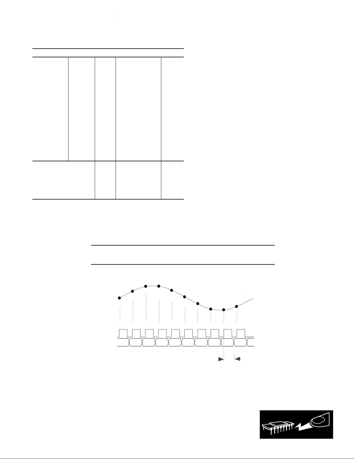
n+2
n+3
n+1
n
Analog
Input
clock
data
n-9 n-8 n-7 n-6 n-5 n-4 n-3 n-2 n-1
out
n+4
n+5
n+6
n+7
n+8
n+9
n
n+1
Tod = 7nsec typ
Figure 1. AD9244 Input Timing
CAUTION
ESD (electrostatic discharge) sensitive device. Electrostatic charges as high as 4000 V readily
accumulate on the human body and test equipment and can discharge without detection. Although
the AD9244 features proprietary ESD protection circuitry, permanent damage may occur on devices
subjected to high energy electrostatic discharges. Therefore, proper ESD precautions are recommended to avoid performance degradation or loss of functionality.
REV. PrD 01/22/02
–5–
WARNING!
ESD SENSITIVE DEVICE

PRELIMINAR Y TECHNICAL DATA
AD9244–SPECIFICATIONS
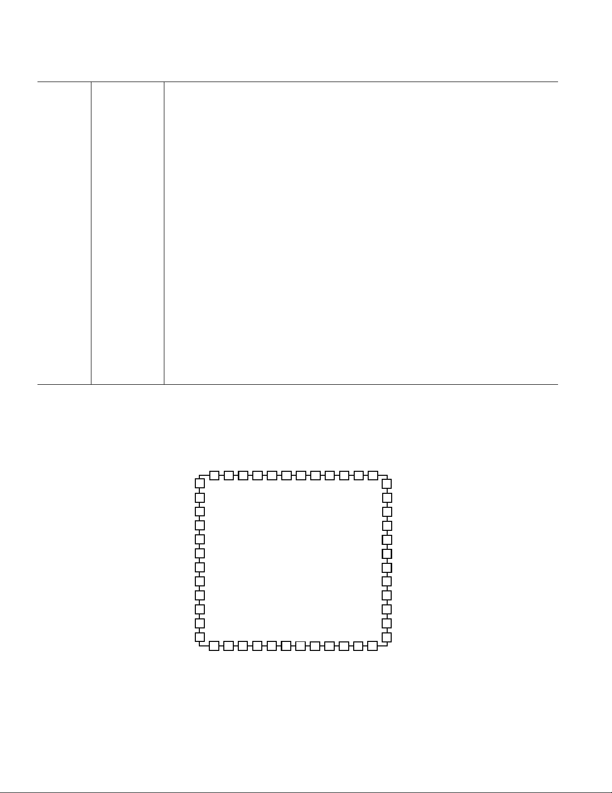
PIN FUNCTION DESCRIPTIONS
Pin
Nunber Name Descriptions
1,2,5,32,33 AGND Analog Ground
3,4,31,34 AVDD Analog Supply Voltage
5 CLKGND Clock Ground
8,44 N C Do not connect
7,6 CLK+,CLK- Differential Clock Input
9 OEB Digital Output Enable (active low)
10 DB0 (LSB) Least Significant Bit, digital output
11-13,16-21
24-26 DB1 - DB12 Digital outputs
27 DB13 (MSB) Most Significant Bit, digital output
14,22,30 DRGND Digital Ground
15,23,29 DRVDD Digital Supply Voltage
28 OTR Out of range indicator (logic 1 indicates OTR)
35 DFS Data Format Select, connect to;
DRGND for straight binary
DRVDD for 2’s complement
36 REFSENSE Internal reference control
37 VREF Internal Reference
38 REFGND Reference ground
39,40,41,42 REFT,REFB Internal ADC reference decoupling
43 DUTY 50% Duty Cycle Restore, (Connect to AVDD to activate 50% duty cycle restore, de-
couple to AGND for external control of both clock edges.)
45 CML Common mode reference (0.5*AVDD)
46,47 V IN +,VIN- Differential analog inputs
48 VR Internal Bias Decoupling
AGND
AGND
AVDD
AVDD
AGND
CLK-
CLK+
NC
OEB
DB0 (LSB)
DB1
DB2
VR
VIN-
VIN+
CML
NC
DUTY
REFT
REFT
REFB
1
2
3
4
5
6
7
(Preliminary and not to scale)
8
9
10
11
12
13 14 15 16 17 18 19 20 21 22 23 24
DB3
DRGND
DRVDD
AD9244
48 LQFP
DB4
DB5
DB6
DB7
DB8
DB9
REFB
REFGND
VREF
373839404142434445464748
REF SENSE
36
DFS
35
AVDD
34
AGND
33
AGND
32
AVDD
31
30
DRGND
29
DRVDD
28
OTR
27
DB13 (MSB)
26
DB12
25
DB11
DRGND
DRVDD
DB10
REV. PrD 01/22/02
–6–
 Loading...