Analog Devices AD9070BR, AD9070-PCB, 5962-9756301HXC Datasheet

10-Bit, 100 MSPS
a
FEATURES
10-Bit, 100 MSPS ADC
Low Power: 600 mW Typical at 100 MSPS
On-Chip Track/Hold
230 MHz Analog Bandwidth
SINAD = 54 dB @ 41 MHz
On-Chip Reference
1 V p-p Analog Input Range
Single Supply Operation: +5 V or –5 V
Differential Clock Input
Available in Standard Military Drawing Version
APPLICATIONS
Digital Communications
Signal Intelligence
Digital Oscilloscopes
Spectrum Analyzers
Medical Imaging
Radar
HDTV
GENERAL DESCRIPTION
The AD9070 is a monolithic sampling analog-to-digital
converter with an on-chip track-and-hold circuit and ECL
digital interfaces. The product operates at a 100 MSPS
conversion rate with outstanding dynamic performance over
its full operating range.
The ADC requires only a single –5 V supply and an encode
clock for full performance operation. The digital outputs are
ECL compatible, while a differential clock input accommodates
a wide range of logic levels. The AD9070 may be operated in a
Positive ECL (PECL) environment with a single +5 V supply.
An Out-of-Range output (OR) is available in the DIP version to
indicate that a conversion result is outside the operating range.
In both package styles, the output data are held at saturation
levels during an out-of-range condition.
A/D Converter
AD9070
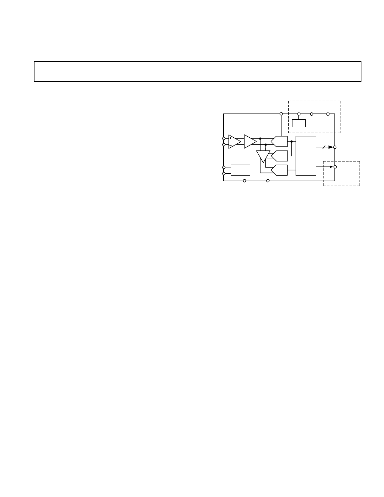
FUNCTIONAL BLOCK DIAGRAM
VREF
VREF
IN
OUT
AIN
AIN
ENCODE
ENCODE
TIMING
V
AD9070
T/H
SUM
AMP
EE
GND
ADC
DAC
ADC
–2.5V
ENCODE
LOGIC
The input amplifier supports single-ended interfaces. An
internal –2.5 V reference is included in the SOIC packaged
device (an external voltage reference is required for the
DIP version).
Fabricated on an advanced bipolar process, the AD9070
is available in a plastic SOIC package specified over the
industrial temperature range (–40°C to +85°C), and a full
MIL-PRF-38534 QML version (–55°C to +125°C) in a
ceramic Dual-in-Line Package (DIP).
COMP
SOIC (BR)
PACKAGE
BYPASS
ONLY
10
REF
D9 – D0
OR
DIP
PACKAGE
ONLY
REV. C
Information furnished by Analog Devices is believed to be accurate and
reliable. However, no responsibility is assumed by Analog Devices for its
use, nor for any infringements of patents or other rights of third parties that
may result from its use. No license is granted by implication or otherwise
under any patent or patent rights of Analog Devices.
One Technology Way, P.O. Box 9106, Norwood, MA 02062-9106, U.S.A.
Tel: 781/329-4700 www.analog.com
Fax: 781/326-8703 © Analog Devices, Inc., 2001

(VEE = –5 V, ENCODE = 100 MSPS, outputs loaded with 100 ⍀ to –2 V unless
AD9070–SPECIFICATIONS
Parameter Temp Level Min Typ Max Min Typ Max Unit
RESOLUTION 10 10 Bit
DC ACCURACY
Differential Nonlinearity 25°CI ± 0.6 +1.25/–1.0 ± 0.6 +1.25/–1.0 LSB
Integral Nonlinearity 25°CI ± 0.6 ± 1.5 ± 0.6 ± 1.5 LSB
No Missing Codes Full VI Guaranteed Guaranteed
Gain Error
Gain Tempco
ANALOG INPUT
Input Voltage Range (with Respect to AIN) Full V ± 512 ± 512 mV p-p
Common-Mode Voltage Full V –2.5 ± 0.2 –2.5 ± 0.2 V
Input Offset Voltage 25°CI ± 7 ± 18 ± 7 ± 18 mV
Input Resistance 25°C I 10 40 10 40 kΩ
Input Capacitance 25° CV 3 3 pF
Input Bias Current 25°C I 75 200 75 200 µA
Analog Bandwidth, Full Power 25°C V 230 230 MHz
1
1
otherwise noted.)
Test AD9070BR 5962-9756301HXC
Full VI ± 0.7 +1.5/–1.0 ±0.9 +2.00/–1.0 LSB
Full VI ± 0.9 ± 1.5 ± 2.25 LSB
25°CI ± 1 ± 4 ± 1 ± 4% FS
Full VI ± 2 ± 6% FS
Full V 115 130 ppm/°C
Full I ± 8 ± 9 ± 20 mV
Full I 40 10 40 kΩ
Full I 75 75 200 µA
REFERENCE OUTPUT
Output Voltage Full VI –2.4 –2.5 –2.6 N/A V
Temperature Coefficient Full V 170 N/A ppm/°C
SWITCHING PERFORMANCE
Maximum Conversion Rate Full VI 100 100 MSPS
Minimum Conversion Rate Full IV 40 40 MSPS
Encode Pulsewidth High (tEH)25°C IV 4.5 13 4.5 13 ns
Encode Pulsewidth Low (t
Aperture Delay (t
)25°C V 0.85 0.85 ns
A
Aperture Uncertainty (Jitter) 25°C V 2.5 2.5 ps rms
Output Valid Time (tV)
Output Propagation Delay (t
Output Rise Time (t
R
)25°C IV 4.5 13 4.5 13 ns
EL
2
2
)
PD
Full VI 1.5 2.6 1.5 2.6 ns
Full VI 3.0 4.0 3.0 4.0 ns
) Full VI 0.5 0.5 1.2 ns
Output Fall Time (tF) Full VI 0.5 0.5 1.2 ns
DIGITAL INPUTS
Logic “1” Voltage Full IV –1.1 –0.4 –1.1 –0.4 V
Logic “0” Voltage Full IV –1.5 –1.5 V
Logic “1” Current Full VI ± 10 ± 10 µA
Logic “0” Current Full VI ± 10 ± 10 µA
Input Capacitance 25° CV 3 3 pF
DIGITAL OUTPUTS
Logic “1” Voltage Full VI –1.1 –1.15 V
Logic “0” Voltage Full VI –1.65 –1.60 V
Output Coding Two’s Complement Two’s Complement
POWER SUPPLY
VEE Supply Current (VEE = –5 V) Full VI 80 120 150 80 120 150 mA
Power Dissipation
Power Supply Sensitivity
3
4
Full VI 400 600 750 400 600 750 mW
25°C I 0.005 0.012 0.005 0.012 V/V
–2–
REV. C

AD9070
Test AD9070BR 5962-9756301HXC
Parameter Temp Level Min Typ Max Min Typ Max Unit
DYNAMIC PERFORMANCE
Transient Response 25°CV 3 3 ns
Overvoltage Recovery Time 25°CV 4 4 ns
Signal-to-Noise Ratio (SNR)
(Without Harmonics)
= 10.3 MHz 25°C I 55 57 55 57 dB
f
IN
fIN = 41 MHz 25°C I 54 56 54 56 dB
Signal-to-Noise Ratio (SINAD)
(With Harmonics)
= 10.3 MHz 25°C I 54 56 54 56 dB
f
IN
fIN = 41 MHz 25°C I 51 54 51 54 dB
Effective Number of Bit
= 10.3 MHz 25°C I 8.8 9.2 8.8 9.2 Bits
f
IN
= 41 MHz 25°C I 8.3 8.9 8.3 8.9 Bits
f
IN
2nd Harmonic Distortion
fIN = 10.3 MHz 25°C I 63 70 63 70 dBc
= 41 MHz 25°C I 58 63 58 63 dBc
f
IN
3rd Harmonic Distortion
fIN = 10.3 MHz 25°C I 65 71 65 71 dBc
= 41 MHz 25°C I 57 61 57 61 dBc
f
IN
Two-Tone Intermod Distortion (IMD)
fIN = 10.3 MHz 25°C V 70 70 dBc
fIN = 41 MHz 25°C V 60 60 dBc
NOTES
1
Gain error and gain temperature coefficient are based on the ADC only (with a fixed –2.5 V external reference).
2
tV and tPD are measured from the threshold crossing of the ENCODE input to the 50% levels of the digital outputs. The output ac load during test is 10 pF.
3
Power dissipation is measured under the following conditions: fS 100 MSPS, analog input is –1 dBFS at 10.3 MHz. Power dissipation does not include the current of
the external ECL pull-down resistors that set the current in the ECL output followers.
4
A change in input offset voltage with respect to a change in VEE.
5
SNR/harmonics based on an analog input voltage of –1.0 dBFS referenced to a 1.024 V full-scale input range.
Typical thermal impedance for the R style (SOIC) 28-lead package: θJC = 23°C/W, θCA = 48°C/W, θJA = 71°C/W.
Typical thermal impedance for the DH style (Ceramic DIP) 28-lead package: θJC = 8°C/W, θCA = 43°C/W, θJA = 51°C/W.
Contact DSCC to obtain the latest revision of the 5962-9756301 drawing.
Specifications subject to change without notice.
5
Full V 56 55 dB
Full V 55 54 dB
Full V 55 54 dB
Full V 53 52 dB
REV. C
AIN
D9–D0
ENCODE
ENCODE
SAMPLE N–1
SAMPLE N SAMPLE N+3 SAMPLE N+4
1/fs
SAMPLE N+2SAMPLE N+1
t
PD
t
V
t
A
t
t
EH
EL
DATA N–4 DATA N–3 DATA N–2 DATA N–1 DATA N DATA N+1
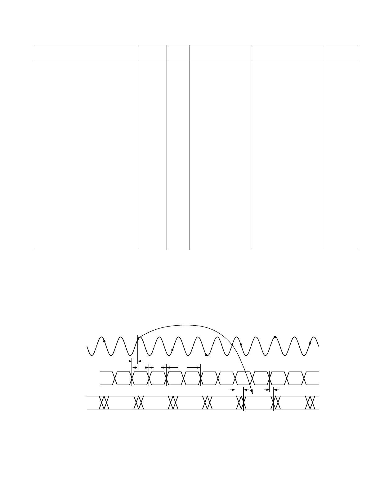
Figure 1. Timing Diagram
–3–

AD9070
ABSOLUTE MAXIMUM RATINGS*
VEE . . . . . . . . . . . . . . . . . . . . . . . . . . . . . . . . . . . . . . . . . –6 V
Analog Inputs . . . . . . . . . . . . . . . . . . . . . V
Digital Inputs . . . . . . . . . . . . . . . . . . . . . . . . . . . V
VREF IN, VREF OUT . . . . . . . . . . . . . . . . . . . . V
–1 V to +1.0 V
EE
to 0.0 V
EE
to 0.0 V
EE
Digital Output Current . . . . . . . . . . . . . . . . . . . . . . . . 20 mA
Operating Temperature . . . . . . . . . . . . . . . . –55°C to +125°C
Storage Temperature . . . . . . . . . . . . . . . . . . –65°C to +150°C
Maximum Junction Temperature . . . . . . . . . . . . . . . . 150°C
Maximum Case Temperature . . . . . . . . . . . . . . . . . . . 150°C
*Stresses above those listed under Absolute Maximum Ratings may cause permanent
damage to the device. This is a stress rating only; functional operation of the device at
these or any other conditions outside of those indicated in the operation sections of this
specification is not implied. Exposure to absolute maximum ratings for extended
periods may affect device reliability.
EXPLANATION OF TEST LEVELS
Test Level
I – 100% production tested.
II – 100% production tested at 25°C and sample tested at
specified temperatures.
III – Sample tested only.
IV – Parameter is guaranteed by design and characteriza-
tion testing.
V – Parameter is a typical value only.
VI – 100% production tested at 25°C; guaranteed by design
and characterization testing for industrial temperature
range; 100% production tested at temperature extremes
for military devices.
Table I. Output Coding
Two’s
Step AIN–AIN Code Complement OR
1024 ≥ 0.512 V >511 01 1111 1111 1
1023 0.511 V 511 01 1111 1111 0
1022 0.510 V 510 01 1111 1110 0
•• • • •
•• • • •
•• • • •
513 0.001 V 1 00 0000 0001 0
512 0.000 V 0 00 0000 0000 0
511 –0.001 V –1 11 1111 1111 0
•• • • •
•• • • •
•• • • •
1 –0.511 V –511 10 0000 0001 0
0 –0.512 V –512 10 0000 0000 0
–1 ≤ –0.513 V <512 10 0000 0000 1
ORDERING GUIDE
Model Temperature Range Package Description Package Option
AD9070BR –40°C to +85°C Small Outline IC (SOIC) R-28
AD9070/PCB 25°C Evaluation Board
5962-9756301HXC –55°C to +125°C Ceramic DIP DH-28
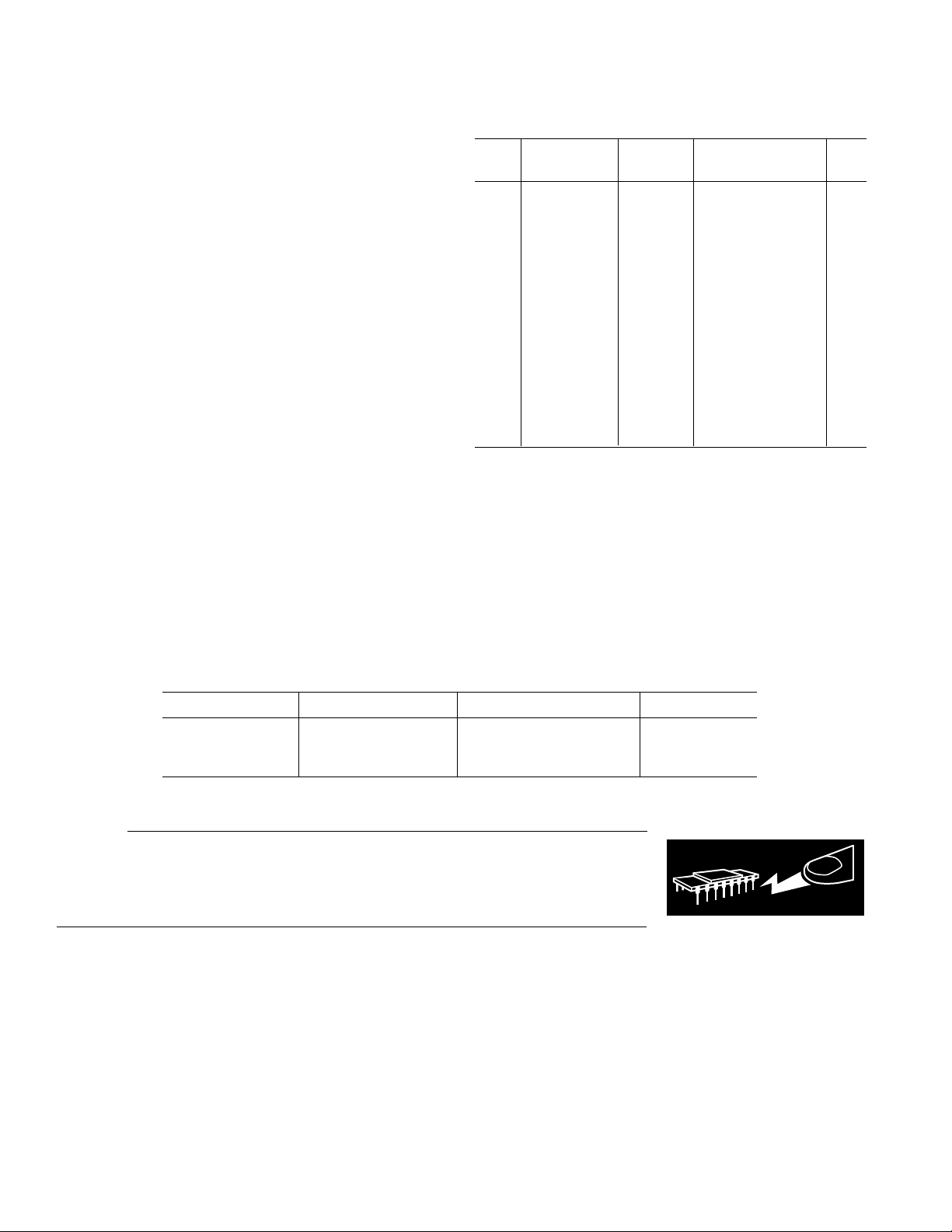
CAUTION
ESD (electrostatic discharge) sensitive device. Electrostatic charges as high as 4000 V readily
accumulate on the human body and test equipment and can discharge without detection.
Although the AD9070 features proprietary ESD protection circuitry, permanent damage may
occur on devices subjected to high-energy electrostatic discharges. Therefore, proper ESD
precautions are recommended to avoid performance degradation or loss of functionality.
WARNING!
ESD SENSITIVE DEVICE
–4–
REV. C

PIN FUNCTION DESCRIPTIONS
Pin Numbers
AD9070BR AD9070DIP
R Package D Package Mnemonic Function
AD9070
1, 7, 12, 21, 23 1, 7, 9, 14, 21 V
EE
Negative Power Supply. Nominally –5.0 V.
2, 8, 11, 20, 22 2, 6, 8, 10, 13, 15, 22 GND Ground
3 N/A VREF OUT Internal Reference Output (–2.5 V typical); Bypass with 0.1 µF to Ground
4 3 VREF IN Reference Input for ADC (–2.5 V typical)
5 N/A COMP Internal Amplifier Compensation, 0.1 µF to V
6 N/A REF BYPASS Reference Bypass Node, 0.1 µF to V
EE
EE
94 AIN Analog Input – Complement
10 5 AIN Analog Input – True
13 11 ENCODE Encode Clock for ADC (ADC Samples on Rising Edge of ENCODE).
14 12 ENCODE Encode Clock Complement (ADC Samples on Falling Edge of ENCODE).
28–24, 19–15 27–23, 20–16 D9–D0 Digital Outputs of ADC. D9 is the MSB. Data is two’s complement.
N/A 28 OR Out-of-Range Output. Goes HIGH when the converted sample is more
positive than 1FFh or more negative than 200h (Two’s Complement Coding).
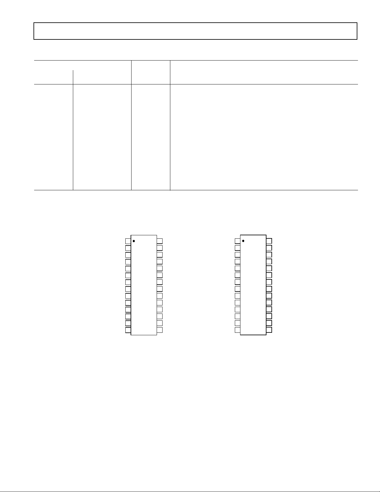
PIN CONFIGURATIONS
SOIC Ceramic DIP
28
27
26
25
24
23
22
21
20
19
18
17
16
15
OR
D9 (MSB)
D8
D7
D6
D5
GND
V
EE
D4
D3
D2
D1
D0 (LSB)
GND
V
GND
VREF OUT
VREF IN
COMP
REF BYPASS
V
GND
AIN
AIN
GND
V
ENCODE
ENCODE
EE
EE
10
11
12
EE
13
14
1
2
3
4
5
6
AD9070BR
7
TOP VIEW
(Not to Scale)
8
9
28
27
26
25
24
23
22
21
20
19
18
17
16
15
D9 (MSB)
D8
D7
D6
D5
V
EE
GND
V
EE
GND
D4
D3
D2
D1
D0 (LSB)
V
GND
VREF IN
AIN
AIN
GND
V
GND
V
GND
ENCODE
ENCODE
GND
V
EE
EE
8
9
EE
10
11
12
13
14
EE
1
2
3
4
5
6
AD9070DIP
7
TOP VIEW
(Not to Scale)
REV. C
–5–
 Loading...