

Low Noise, Precision 16 V CMOS,
O
www.BDTIC.com/ADI
FEATURES
Low offset voltage: 100 μV maximum @ VS = 5 V
Low input bias current: 1 pA maximum
Single-supply operation: 5 V to 16 V
Low noise: 10 nV/√Hz
Wide bandwidth: 4 MHz
Unity-gain stable
Small package options
3 mm × 3 mm 8-lead LFCSP
8-lead MSOP and narrow SOIC
14-lead TSSOP and narrow SOIC
APPLICATIONS
Sensors
Medical equipment
Consumer audio
Photodiode amplification
ADC drivers
Rail-to-Rail Operational Amplifiers
AD8661/AD8662/AD8664
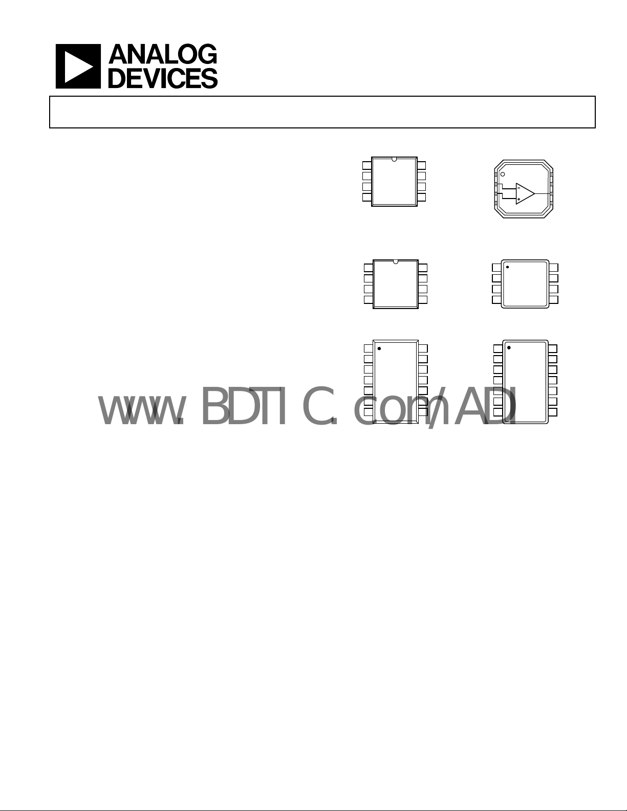
PIN CONFIGURATIONS
1
NC
AD8661
–IN
2
TOP VIEW
3
+IN
(Not to Scale)
V–
4
NC = NO CONNECT
Figure 1. AD8661, 8-Lead SOIC_N
1
OUT A
–IN A
+IN A
V–
AD8662
2
TOP VIEW
3
(Not to Scale)
4
Figure 3. AD8662, 8-Lead SOIC_N
1
OUT A
–IN A
2
AD8664
3
+IN A
+IN B
–IN B
OUT B
V+
TOP VIEW
(Not to Scale)
4
5
6
7
(R-8)
(R-8)
8
7
6
5
14
13
12
11
10
8
7
6
5
9
8
NC
V+
OUT
NC
V+
OUT B
–IN B
+IN B
OUT D
–IN D
+IN D
V–
+IN C
–IN C
OUT C
1NC
AD8661
2–IN
3+IN
05200-002
4V–
NC = NO CONNECT
Figure 2. AD8661, 8-Lead LFCSP_VD
(CP-8-
OUT A
1
AD8662
2
–IN A
+IN A
05200-001
V–
TOP VIEW
3
(Not to Scale)
4
Figure 4. AD8662, 8-Lead MSOP
(RM-8)
1
OUT A
–IN A
2
V+
AD8664
3
TOP VIEW
(Not to Scale)
4
5
6
7
+IN A
+IN B
–IN B
UT B
8NC
7V+
6OUT
5NC
05200-035
2)
V+
8
7
OUT B
–IN B
6
5
+IN B
OUT D
14
–IN D
13
+IN D
12
V–
11
10
+IN C
9
–IN C
8
OUT C
05200-004
GENERAL DESCRIPTION
The AD8661/AD8662/AD8664 are rail-to-rail output, singlesupply amplifiers that use the Analog Devices, Inc., patented
DigiTrim® trimming technique to achieve low offset voltage.
The AD866x series features extended operating ranges, with
supply voltages up to 16 V. It also features low input bias
current, wide signal bandwidth, and low input voltage and
current noise.
The combination of low offset, very low input bias current, and
ide supply range makes these amplifiers useful in a wide
a w
variety of applications usually associated with higher priced
JFET amplifiers. Systems using high impedance sensors, such as
photodiodes, benefit from the combination of low input bias
current, low noise, low offset, and wide bandwidth. The wide
operating voltage range meets the demands of high
performance ADCs and DACs. Audio applications and medical
05200-036
Figure 5. AD8664, 14-Lead SOIC_N
-14)
(R
Figure 6. AD8664, 14-Lead TSSOP
(RU-14)
monitoring equipment can take advantage of the high input
impedance, low voltage and current noise, and wide bandwidth.
The single AD8661 is available in a narrow 8-lead SOIC
p
ackage and a very thin, dual lead, 8-lead LFCSP. The AD8661
SOIC_N package is specified over the extended industrial
temperature range of −40°C to +125°C. The AD8661
LFCSP_VD is specified over the industrial temperature range
of −40°C to +85°C. The AD8662 is available in a narrow 8-lead
SOIC package and an 8-lead MSOP, both specified over the
extended industrial temperature range of −40°C to +125°C. The
AD8664 is available in a narrow 14-lead SOIC package and a
14-lead TSSOP, both with an extended industrial temperature
range of −40°C to +125°C.
05200-037
Rev. D
Information furnished by Analog Devices is believed to be accurate and reliable. However, no
responsibility is assumed by Anal og Devices for its use, nor for any infringements of patents or ot her
rights of third parties that may result from its use. Specifications subject to change without notice. No
license is granted by implication or otherwise under any patent or patent rights of Analog Devices.
Trademarks and registered trademarks are the property of their respective owners.
One Technology Way, P.O. Box 9106, Norwood, MA 02062-9106, U.S.A.
Tel: 781.329.4700 www.analog.com
Fax: 781.461.3113 ©2006 Analog Devices, Inc. All rights reserved.

AD8661/AD8662/AD8664
www.BDTIC.com/ADI
TABLE OF CONTENTS
Features.............................................................................................. 1
AD8661 Electrical Characteristics—LFCSP_VD Only............5
Applications....................................................................................... 1
Pin Configurations ........................................................................... 1
General Description ......................................................................... 1
Revision History ............................................................................... 2
Specifications..................................................................................... 3
AD8661/AD8662/AD8664 Electrical Characteristics—
SOIC_N, MSOP, and TSSOP ...................................................... 3
AD8661/AD8662/AD8664 Electrical Characteristics—
SOIC_N, MSOP, and TSSOP ...................................................... 4
REVISION HISTORY
7/06—Rev. C to Rev. D
Added AD8664 ...................................................................Universal
Added 14-Lead SOIC_N and 14-Lead TSSOP ...............Universal
Changes to Features.......................................................................... 1
Changes to Table 1............................................................................ 3
Changes to Table 2............................................................................ 4
Changes to Table 3............................................................................ 5
Changes to Table 4............................................................................ 6
Changes to Table 5 and Table 6....................................................... 7
Changes to Figure 29...................................................................... 11
Updated Outline Dimensions....................................................... 13
Changes to Ordering Guide.......................................................... 15
5/06—Rev. B to Rev. C
hanges to Ordering Guide.......................................................... 13
C
3/06—Rev. A to Rev. B
A
dded AD8662 ...................................................................Universal
Added MSOP ......................................................................Universal
AD8661 Electrical Characteristics—LFCSP_VD Only............6
Absolute Maximum Ratings ............................................................7
Thermal Resistance.......................................................................7
ESD Caution...................................................................................7
Typical Performance Characteristics..............................................8
Outline Dimensions....................................................................... 13
Ordering Guide .......................................................................... 15
Changes to Table 1.............................................................................3
C
hanges to Table 2.............................................................................4
Changes to Table 3.............................................................................5
Changes to Table 4.............................................................................6
Changes to Table 5.............................................................................7
Updated Outline Dimensions....................................................... 13
Changes to Ordering Guide.......................................................... 13
1/06—Rev. 0 to Rev. A
dded LFCSP_VD .............................................................Universal
A
Changes to Table 1.............................................................................3
Changes to Table 2.............................................................................4
Changes to Ordering Guide.......................................................... 13
9/05—Revision 0: Initial Version
Rev. D | Page 2 of 16
AD8661/AD8662/AD8664
www.BDTIC.com/ADI
SPECIFICATIONS
AD8661/AD8662/AD8664 ELECTRICAL CHARACTERISTICS—SOIC_N, MSOP, AND TSSOP
VS = 5.0 V, VCM = VS/2, TA = 25°C, unless otherwise noted.
Table 1.
Parameter Symbol Conditions Min Typ Max Unit
INPUT CHARACTERISTICS
Offset Voltage VOS V
AD8661 −40°C < TA < +85°C 1000 μV
AD8661 −40°C < TA < +125°C 1400 μV
AD8662 −40°C < TA < +125°C 1000 μV
AD8664 −40°C < TA < +125°C 1200 μV
Input Bias Current IB 0.3 1 pA
−40°C < TA < +85°C 50 pA
−40°C < TA < +125°C 300 pA
Input Offset Current IOS 0.2 0.5 pA
−40°C < TA < +85°C 20 pA
−40°C < TA < +125°C 75 pA
Input Voltage Range −0.1 +3.0 V
Common-Mode Rejection Ratio CMRR VCM = −0.1 V to +3.0 V 85 100 dB
−40°C < TA < +125°C 80 100 dB
Large Signal Voltage Gain AVO R
Offset Voltage Drift TCVOS
AD8661 −40°C < TA < +125°C 3 10 μV/°C
AD8662, AD8664 −40°C < TA < +125°C 2 9 μV/°C
OUTPUT CHARACTERISTICS
Output Voltage High VOH I
−40°C < TA < +125°C 4.80 V
Output Voltage Low VOL I
−40°C < TA < +125°C 110 mV
Short-Circuit Current ISC ±19 mA
Closed-Loop Output Impedance Z
POWER SUPPLY
Supply Current per Amplifier ISY V
−40°C < TA < +125°C 2.0 mA
DYNAMIC PERFORMANCE
Slew Rate SR RL = 2 kΩ 3.5 V/μs
Gain Bandwidth Product GBP 4 MHz
Phase Margin ΦO 65 Degrees
NOISE PERFORMANCE
Peak-to-Peak Noise en p-p f = 0.1 Hz to 10 Hz 2.5 μV p-p
Voltage Noise Density e
f = 10 kHz 10 nV/√Hz
Current Noise Density i
f = 1 MHz, AV = 1 50 Ω
OUT
n
n
= VS/2 30 100 μV
CM
= 2 kΩ, VO = 0.5 V to 4.5 V 100 220 V/mV
L
= 1 mA 4.85 4.93 V
L
= 1 mA 50 100 mV
L
= VS/2 1.15 1.40 mA
O
f = 1 kHz 12 nV/√Hz
f = 1 kHz 0.1 pA/√Hz
Rev. D | Page 3 of 16
AD8661/AD8662/AD8664
www.BDTIC.com/ADI
AD8661/AD8662/AD8664 ELECTRICAL CHARACTERISTICS—SOIC_N, MSOP, AND TSSOP
VS = 16.0 V, VCM = VS/2, TA = 25°C, unless otherwise noted.
Table 2.
Parameter Symbol Conditions Min Typ Max Unit
INPUT CHARACTERISTICS
Offset Voltage VOS V
AD8661 −40°C < TA < +85°C 1000 μV
AD8661 −40°C < TA < +125°C 1400 μV
AD8662 −40°C < TA < +125°C 1000 μV
AD8664 −40°C < TA < +125°C 1200 μV
Input Bias Current IB 0.3 1 pA
−40°C < TA < +85°C 50 pA
−40°C < TA < +125°C 300 pA
Input Offset Current IOS 0.2 0.5 pA
−40°C < TA < +85°C 20 pA
−40°C < TA < +125°C 75 pA
Input Voltage Range −0.1 +14.0 V
Common-Mode Rejection Ratio CMRR VCM = −0.1 V to +14.0 V 90 110 dB
−40°C < TA < +125°C 90 110 dB
Large Signal Voltage Gain AVO R
Offset Voltage Drift TCVOS
AD8661 −40°C < TA < +125°C 3 10 μV/°C
AD8662, AD8664 −40°C < TA < +125°C 2 9 μV/°C
OUTPUT CHARACTERISTICS
Output Voltage High VOH I
I
−40°C < TA < +125°C 15.50 V
Output Voltage Low VOL I
I
−40°C < TA < +125°C 350 mV
Short-Circuit Current ISC ±140 mA
Closed-Loop Output Impedance Z
POWER SUPPLY
Power Supply Rejection Ratio PSRR VS = 5 V to 16 V 95 110 dB
−40°C < TA < +125°C 95 115 dB
Supply Current per Amplifier ISY V
−40°C < TA < +125°C 2.1 mA
DYNAMIC PERFORMANCE
Slew Rate SR RL = 2 kΩ 3.5 V/μs
Gain Bandwidth Product GBP 4 MHz
Phase Margin ΦO 65 Degrees
NOISE PERFORMANCE
Peak-to-Peak Noise en p-p f = 0.1 Hz to 10 Hz 2.5 μV p-p
Voltage Noise Density e
f = 10 kHz 10 nV/√Hz
Current Noise Density i
f = 1 MHz, AV = 1 45 Ω
OUT
n
n
= VS/2 50 160 μV
CM
= 2 kΩ, VO = 0.5 V to 15.5 V 200 360 V/mV
L
= 1 mA 15.93 15.97 V
L
= 10 mA 15.60 15.70 V
L
= 1 mA 24 50 mV
L
= 10 mA 190 300 mV
L
= VS/2 1.25 1.55 mA
O
f = 1 kHz 12 nV/√Hz
f = 1 kHz 0.1 pA/√Hz
Rev. D | Page 4 of 16

AD8661/AD8662/AD8664
www.BDTIC.com/ADI
AD8661 ELECTRICAL CHARACTERISTICS—LFCSP_VD ONLY
VS = 5.0 V, VCM = VS/2, TA = 25°C, unless otherwise noted.
Table 3.
Parameter Symbol Conditions Min Typ Max Unit
INPUT CHARACTERISTICS
Offset Voltage VOS V
−40°C < TA < +85°C 2000 μV
Input Bias Current IB 0.3 1 pA
−40°C < TA < +85°C 50 pA
Input Offset Current IOS 0.2 0.5 pA
−40°C < TA < +85°C 20 pA
Input Voltage Range −0.1 +3.0 V
Common-Mode Rejection Ratio CMRR VCM = −0.1 V to +3.0 V 85 100 dB
−40°C < TA < +85°C 80 100 dB
Large Signal Voltage Gain AVO R
Offset Voltage Drift TCVOS −40°C < TA < +85°C 4 17 μV/°C
OUTPUT CHARACTERISTICS
Output Voltage High VOH I
−40°C < TA < +85°C 4.80 V
Output Voltage Low VOL I
−40°C < TA < +85°C 120 mV
Short-Circuit Current ISC ±19 mA
Closed-Loop Output Impedance Z
POWER SUPPLY
Supply Current per Amplifier ISY V
−40°C < TA < +85°C 1.8 mA
DYNAMIC PERFORMANCE
Slew Rate SR RL = 2 kΩ 3.5 V/μs
Gain Bandwidth Product GBP 4 MHz
Phase Margin ΦO 65 Degrees
NOISE PERFORMANCE
Peak-to-Peak Noise en p-p f = 0.1 Hz to 10 Hz 2.5 μV p-p
Voltage Noise Density e
f = 10 kHz 10 nV/√Hz
Current Noise Density i
f = 1 MHz, AV = 1 65 Ω
OUT
n
n
= VS/2 50 300 μV
CM
= 2 kΩ, VO = 0.5 V to 4.5 V 100 240 V/mV
L
= 1 mA 4.85 4.93 V
L
= 1 mA 50 100 mV
L
= VS/2 1.15 1.40 mA
O
f = 1 kHz 12 nV/√Hz
f = 1 kHz 0.1 pA/√Hz
Rev. D | Page 5 of 16

AD8661/AD8662/AD8664
www.BDTIC.com/ADI
AD8661 ELECTRICAL CHARACTERISTICS—LFCSP_VD ONLY
VS = 16.0 V, VCM = VS/2, TA = 25°C, unless otherwise noted.
Table 4.
Parameter Symbol Conditions Min Typ Max Unit
INPUT CHARACTERISTICS
Offset Voltage VOS V
−40°C < TA < +85°C 2000 μV
Input Bias Current IB 0.3 1 pA
−40°C < TA < +85°C 50 pA
Input Offset Current IOS 0.2 0.5 pA
−40°C < TA < +85°C 20 pA
Input Voltage Range −0.1 +14.0 V
Common-Mode Rejection Ratio CMRR VCM = −0.1 V to +14.0 V 90 110 dB
−40°C < TA < +85°C 90 110 dB
Large Signal Voltage Gain AVO R
Offset Voltage Drift TCVOS −40°C < TA < +85°C 4 17 μV/°C
OUTPUT CHARACTERISTICS
Output Voltage High VOH I
I
−40°C < TA < +85°C 15.50 V
Output Voltage Low VOL I
I
−40°C < TA < +85°C 400 mV
Short-Circuit Current ISC ±140 mA
Closed-Loop Output Impedance Z
POWER SUPPLY
Power Supply Rejection Ratio PSRR VS = 5 V to 16 V 95 110 dB
−40°C < TA < +85°C 95 115 dB
Supply Current per Amplifier ISY V
−40°C < TA < +85°C 1.9 mA
DYNAMIC PERFORMANCE
Slew Rate SR RL = 2 kΩ 3.5 V/μs
Gain Bandwidth Product GBP 4 MHz
Phase Margin ΦO 65 Degrees
NOISE PERFORMANCE
Peak-to-Peak Noise en p-p f = 0.1 Hz to 10 Hz 2.5 μV p-p
Voltage Noise Density e
f = 10 kHz 10 nV/√Hz
Current Noise Density i
f = 1 MHz, AV = 1 45 Ω
OUT
n
n
= VS/2 50 300 μV
CM
= 2 kΩ, VO = 0.5 V to 15.5 V 200 420 V/mV
L
= 1 mA 15.95 15.97 V
L
= 10 mA 15.60 15.70 V
L
= 1 mA 24 50 mV
L
= 10 mA 210 350 mV
L
= VS/2 1.25 1.55 mA
O
f = 1 kHz 12 nV/√Hz
f = 1 kHz 0.1 pA/√Hz
Rev. D | Page 6 of 16

AD8661/AD8662/AD8664
www.BDTIC.com/ADI
ABSOLUTE MAXIMUM RATINGS
Table 5.
Parameter Rating
Supply Voltage 18 V
Input Voltage −0.1 V to VS
Differential Input Voltage 18 V
Output Short-Circuit Duration to GND Indefinite
Storage Temperature Range −60°C to +150°C
Operating Temperature Range
R-8, RM-8, R-14, and RU-14 −40°C to +125°C
CP-8-2 −40°C to +85°C
Junction Temperature Range −65°C to +150°C
Lead Temperature, Soldering (60 sec) 300°C
Stresses above those listed under Absolute Maximum Ratings
may cause permanent damage to the device. This is a stress
rating only; functional operation of the device at these or any
other conditions above those indicated in the operational
section of this specification is not implied. Exposure to absolute
maximum rating conditions for extended periods may affect
device reliability.
THERMAL RESISTANCE
θJA is specified for the worst-case conditions, that is, a device
soldered in a circuit board for surface-mount packages.
Table 6. Thermal Resistance
Package Type θJA θ
8-Lead SOIC_N 121 43 °C/W
8-Lead LFCSP_VD 75
8-Lead MSOP 142 44 °C/W
14-Lead SOIC_N 88.2 56.3 °C/W
14-Lead TSSOP 114 23.3 °C/W
1
Exposed pad soldered to application board.
1
Unit
JC
1
18
°C/W
ESD CAUTION
ESD (electrostatic discharge) sensitive device. Electrostatic charges as high as 4000 V readily accumulate on
the human body and test equipment and can discharge without detection. Although this product features
proprietary ESD protection circuitry, permanent damage may occur on devices subjected to high energy
electrostatic discharges. Therefore, proper ESD precautions are recommended to avoid performance
degradation or loss of functionality.
Rev. D | Page 7 of 16

AD8661/AD8662/AD8664
www.BDTIC.com/ADI
TYPICAL PERFORMANCE CHARACTERISTICS
6000
VS= 16V
= 25°C
T
A
= –0.1V TO +14V
V
CM
5000
300
VS= 5V AND 16V
250
4000
3000
2000
NUMBER OF AMPL IFIE RS
1000
0
–150
VOS(µV)
Figure 7. Input Offset Voltage Distribution
16
14
12
10
8
6
NUMBER OF AMPL IFIE RS
4
2
0
0123456789
TCVOS(µV/°C)
VS= 16V
= –40°C TO +125°C
T
A
=8V
V
CM
Figure 8. Offset Voltage Drift Distribution
200
150
100
INPUT BIAS CURRENT (pA)
50
05200-026
150100500–50–100
0
–40
TEMPERATURE (°C)
05200-032
1201008040 60200–20
Figure 10. Input Bias Current vs. Temperature
10k
VDD= 16V
1k
100
10
1
OUTPUT SAT URATION VO LTAGE (mV)
05200-017
10
0.1
0.001 0.01 0.1 1 10
VDD–V
OH
SOURCING
V
SINKING
LOAD CURRENT (mA)
OL
05200-019
100
Figure 11. Output Swing Saturation Voltage vs. Load Current
300
VS=16V
T
=25°C
A
200
100
(µV)
0
OS
V
–100
–200
–300
0
COMMON-MO DE VOLT AGE (V)
Figure 9. Input Offset Voltage vs. Common-Mode Voltage
05200-023
1412 131110987654321
110
IL = 1mA
100
90
80
70
60
50
40
30
20
OUTPUT SAT URATION VO LTAGE (mV)
10
0
–40
(VDD – VOH) AT VS = 5V
TEMPERATURE ( °C)
Figure 12. Output Swing Saturation Voltage vs. Temperature, I
Rev. D | Page 8 of 16
VOL AT VS = 5V
(VDD – VOH) AT VS = 16V
V
AT VS = 16V
OL
1201008040 60200–20
= 1 mA
L
05200-030

AD8661/AD8662/AD8664
www.BDTIC.com/ADI
450
IL = 10mA
400
350
(VDD – VOH) AT VS = 16V
300
250
200
150
100
OUTPUT SAT URATION VO LTAGE (mV)
50
0
–40
TEMPERATURE ( °C)
AT VS = 16V
V
OL
Figure 13. Output Swing Saturation Voltage vs. Temperature, I
1201008040 60200–20
= 10 mA
L
05200-031
140
120
100
80
60
CMRR (dB)
40
20
0
100 1k
VS=5VAND16V
FREQUENCY (Hz)
Figure 16. CMRR vs. Frequency
05200-006
10M1M100k10k
80
VS= 5V AND 16V
R
=100kΩ
L
C
=15pF
L
60
40
20
0
–20
OPEN-LOOP GAIN (dB)
–40
–60
10k 100k 1M 10M
GAIN
FREQUENCY (Hz)
Figure 14. Open-Loop Gain and Phase Shift vs. Frequency
1k
VDD = 16V
100
AV = 100
10
(Ω)
OUT
Z
1
0.1
AV = 10
AV = 1
PHASE
0
45
90
135
180
225
270
315
140
VS= 5V AND 16V
120
100
80
60
PSRR (dB)
40
OPEN-LOOP PHASE SHIFT (Degrees)
05200-003
20
0
1k
FREQUENCY (Hz)
05200-005
10M1M100k10k
Figure 17. PSRR vs. Frequency
70
VS = ±2.5 AND ±8V
G = +1
60
R
= 100kΩ
L
50
40
30
OS+
20
SMALL SIGNAL OVERSHOOT (%)
10
OS–
0.01
100 1k
Figure 15. Closed-Loop Outpu
FREQUENCY (Hz)
t Impedance vs. Frequency
05200-007
10M1M100k10k
0
10
Figure 18. Small Signal Overshoot vs. Load Capacitance
Rev. D | Page 9 of 16
LOAD CAPACITANCE (p F)
05200-015
1k100

AD8661/AD8662/AD8664
V
www.BDTIC.com/ADI
1.8
1.6
1.4
1.2
1.0
(mA)
0.8
SY
I
0.6
0.4
0.2
0
–40
Figure 19. Supply Current vs. Temperature
VS=16V
VS=5V
TEMPERATURE (°C)
100
VS= 5V AND 16V
V
= 100mV
80
IN
C
= 200pF
L
G=+1
60
40
20
0
–20
–40
OUTPUT VO LTAGE ( mV)
–60
–80
05200-029
1201008040 60200–20
–100
TIME (0.5µs/DIV)
05200-010
Figure 22. Small Signal Transient Response
1400
1200
1000
800
(µA)
SY
I
600
400
200
0
0
2.0
VS= ±2.5V AND ±8V
1.5
1.0
0.5
0
–0.5
VS (V)
Figure 20. Supply Current vs. Supply Voltage
(Dual-S
upply Configuration), T
= 25°C
A
8
VS= 16V
C
= 200pF
L
6
4
2
0
–2
OUTPUT VOLTAGE (V)
–4
–6
05200-027
18161412108642
–8
TIME (2µs/DIV)
05200-034
Figure 23. Large Signal Transient Response
100m
V
IN
0V
0V
VS = 16V
G = –100
–1.0
PEAK-TO-PE AK NOISE (µV)
–1.5
–2.0
TIME (1s/DIV)
Figure 21. 0.1 Hz to 10 Hz Input Voltage Noise
05200-009
–8V
V
O
Figure 24. Positive Overload Recovery
Rev. D | Page 10 of 16
TIME (5µs/DIV)
05200-013

AD8661/AD8662/AD8664
www.BDTIC.com/ADI
–100mV
16
0V
V
IN
8V
V
O
VS = 16V
G = –100
NUMBER OF AMPL IFIE RS
14
12
10
8
6
4
VS=5V
T
= –40°C T O +125° C
A
V
=2.5V
CM
0V
TIME (5µs/DIV)
Figure 25. Negative Overload Recovery
1k
VS= ±2.5V AND ±8V
100
10
VOLTAG E NOISE DENSITY (nV/ Hz)
1
1
FREQUENCY (Hz)
Figure 26. Voltage Noise Density vs. Frequency
1800
VS=5V
= 25°C
T
A
NUMBER OF AMPL IFIE RS
1600
1400
1200
1000
800
600
400
200
0
–150
V
= –0.1V TO +3V
CM
VOS(µV)
Figure 27. Input Offset Voltage Distribution
2
05200-014
0
0
TCVOS(µV/°C)
05200-022
10987654321
Figure 28. Offset Voltage Drift Distribution
200
VS = 5V
= 25°C
T
A
150
100
50
(µV)
0
OS
V
–50
–100
–150
05200-008
10k1k10010
–200
COMMON-MODE VOLTAGE (V)
05200-021
3.53.02.52.01.51.00–0.5 0.5
Figure 29. Input Offset Voltage vs. Common-Mode Voltage
10k
VDD=5V
1k
100
10
1
OUTPUT SAT URATION VO LTAGE (mV)
05200-024
150100500–50–100
0.1
0.001 0.01 0.1 1 10 20
VDD–V
OH
SOURCING
LOAD CURRENT (mA)
V
OL
SINKING
05200-020
Figure 30. Output Swing Saturation Voltage vs. Load Current
Rev. D | Page 11 of 16

AD8661/AD8662/AD8664
www.BDTIC.com/ADI
1k
VDD = 5V
100
AV = 100
10
(Ω)
OUT
Z
1
AV = 10
AV = 1
V
IN
VS = 16V
G = +1
V
O
0.1
0.01
100 1k
Figure 31. Closed-Loop Outpu
2.5
VS=±2.5V
C
= 200pF
L
2.0
G=+1
1.5
1.0
0.5
0
–0.5
–1.0
OUTPUT VO LTAGE (V )
–1.5
–2.0
–2.5
FREQUENCY (Hz)
t Impedance vs. Frequency
TIME (1µs/DIV)
05200-033
10M1M100k10k
05200-011
OUTPUT VOLTAGE (2V/DIV)
05200-012
TIME (0.2µs/DIV)
Figure 33. No Phase Reversal
Figure 32. Large Signal Transient Response
Rev. D | Page 12 of 16

AD8661/AD8662/AD8664
www.BDTIC.com/ADI
OUTLINE DIMENSIONS
5.00 (0.1968)
4.80 (0.1890)
4.00 (0.1574)
3.80 (0.1497)
0.25 (0.0098)
0.10 (0.0040)
COPLANARIT Y
0.10
CONTROL LING DI MENSIO NS ARE IN MILLIMETERS; INCH DIMENSIONS
(IN PARENTHESES) ARE ROUNDED-OFF M ILLI METER EQ UIVALENTS FOR
REFERENCE O NLY AND ARE NOT APPROPRIATE FO R USE IN DESIGN.
85
1
1.27 (0.0500)
SEATING
PLANE
COMPLIANT TO JEDEC STANDARDS MS-012-A A
BSC
6.20 (0.2440)
5.80 (0.2284)
4
1.75 (0.0688)
1.35 (0.0532)
0.51 (0.0201)
0.31 (0.0122)
8°
0°
0.25 (0.0098)
0.17 (0.0067)
0.50 (0.0196)
0.25 (0.0099)
1.27 (0.0500)
0.40 (0.0157)
45°
060506-A
Figure 34. 8-Lead Small Outline Package [SOIC_N]
row Body
Nar
(R-8)
Dimensions shown in millimeters and (inches)
0.50
0.40
0.30
4
PIN 1
INDICATOR
1
1.89
1.50
1.74
REF
1.59
PIN 1
INDICATOR
3.00
BSC SQ
TOP
VIEW
2.75
BSC SQ
0.50
BSC
0.60 MAX
8
5
1.60
1.45
1.30
0.90 MAX
0.85 NOM
SEATING
PLANE
12° MAX
0.30
0.23
0.18
0.70 MAX
0.65 TYP
0.05 MAX
0.01 NOM
0.20 REF
Figure 35. 8-Lead Lead Frame Chip Scale Package [LFCSP_VD]
mm x 3 mm Body, Very Thin, Dual Lead
3
(CP-8-2)
Dimensions shown in millimeters
Rev. D | Page 13 of 16

AD8661/AD8662/AD8664
www.BDTIC.com/ADI
0.95
0.85
0.75
0.15
0.00
COPLANARITY
3.20
3.00
2.80
8
5
4
SEATING
PLANE
5.15
4.90
4.65
1.10 MAX
0.23
0.08
3.20
3.00
1
2.80
PIN 1
0.65 BSC
0.38
0.22
0.10
COMPLIANT TO JEDEC STANDARDS MO-187-AA
8°
0°
0.80
0.60
0.40
Figure 36. 8-Lead Mini Small Outline Package [MSOP]
(RM-8)
Dim
ensions shown in millimeters
8.75 (0.3445)
8.55 (0.3366)
4.00 (0.1575)
3.80 (0.1496)
14
1
8
7
6.20 (0.2441)
5.80 (0.2283)
0.25 (0.0098)
0.10 (0.0039)
COPLANARITY
0.10
CONTROLL ING DIMENSI ONS ARE IN MILLIMETERS; INCH DIME NSIONS
(IN PARENTHESES) ARE ROUNDED-OF F MILL IMETER EQ UIVALENTS FOR
REFERENCE ONLY AND ARE NOT APPROPRIATE FOR USE IN DESIGN.
1.27 (0.0500)
BSC
0.51 (0.0201)
0.31 (0.0122)
COMPLIANT TO JEDEC STANDARDS MS-012-AB
1.75 (0.0689)
1.35 (0.0531)
SEATING
PLANE
8°
0°
0.25 (0.0098)
0.17 (0.0067)
0.50 (0.0197)
0.25 (0.0098)
1.27 (0.0500)
0.40 (0.0157)
45°
060606-A
Figure 37. 14-Lead Standard Small Outline Package [SOIC_N]
Nar
row Body
(R-14)
Dimensions shown in millimeters and (inches)
5.10
5.00
4.90
14
4.50
4.40
4.30
PIN 1
1.05
1.00
0.80
0.65
BSC
0.15
0.05
COMPLIANT TO JEDEC STANDARDS MO-153-AB-1
Figure 38. 14-Lead Thin Shrink S
8
6.40
BSC
71
0.20
1.20
0.09
MAX
0.30
SEATING
0.19
PLANE
COPLANARITY
0.10
mall Outline Package [TSSOP]
(RU-14)
Dimensions shown in millimeters
8°
0°
0.75
0.60
0.45
Rev. D | Page 14 of 16

AD8661/AD8662/AD8664
www.BDTIC.com/ADI
ORDERING GUIDE
Model Temperature Range Package Description Package Option Branding
AD8661ARZ
AD8661ARZ-REEL
AD8661ARZ-REEL7
AD8661ACPZ-R2
AD8661ACPZ-REEL
AD8661ACPZ-REEL7
AD8662ARZ
AD8662ARZ-REEL
AD8662ARZ-REEL7
AD8662ARMZ-R2
AD8662ARMZ-REEL
AD8664ARZ
AD8664ARZ-REEL
AD8664ARZ-REEL7
AD8664ARUZ
AD8664ARUZ-REEL
1
Z = Pb-free part.
1
1
1
1
1
1
1
1
1
1
1
1
1
1
1
1
−40°C to +125°C 8-Lead SOIC_N R-8
−40°C to +125°C 8-Lead SOIC_N R-8
−40°C to +125°C 8-Lead SOIC_N R-8
−40°C to +85°C 8-Lead LFCSP_VD CP-8-2 A0M
−40°C to +85°C 8-Lead LFCSP_VD CP-8-2 A0M
−40°C to +85°C 8-Lead LFCSP_VD CP-8-2 A0M
−40°C to +125°C 8-Lead SOIC_N R-8
−40°C to +125°C 8-Lead SOIC_N R-8
−40°C to +125°C 8-Lead SOIC_N R-8
−40°C to +125°C 8-Lead MSOP RM-8 A10
−40°C to +125°C 8-Lead MSOP RM-8 A10
−40°C to +125°C 14-Lead SOIC_N R-14
−40°C to +125°C 14-Lead SOIC_N R-14
−40°C to +125°C 14-Lead SOIC_N R-14
−40°C to +125°C 14-Lead TSSOP RU-14
−40°C to +125°C 14-Lead TSSOP RU-14
Rev. D | Page 15 of 16

AD8661/AD8662/AD8664
www.BDTIC.com/ADI
NOTES
©2006 Analog Devices, Inc. All rights reserved. Trademarks and
registered trademarks are the property of their respective owners.
D05200-0-7/06(D)
Rev. D | Page 16 of 16
 Loading...