

CMOS Single-Supply, Rail-to-Rail Input/Output
O
FEATURES
Single-supply operation: 2.5 V to 6 V
High output current: ±250 mA
Extremely low shutdown supply current: 100 nA
Low supply current: 750 μA/Amp
Wide bandwidth: 3 MHz
Slew rate: 5 V/μs
No phase reversal
Very low input bias current
High impedance outputs when in shutdown mode
Unity-gain stable
APPLICATIONS
Mobile communication handset audio
PC audio
PCMCIA/modem line driving
Battery-powered instrumentation
Data acquisition
ASIC input or output amplifiers
LCD display reference level drivers
GENERAL DESCRIPTION
The AD8591, AD8592, and AD8594 are single, dual, and quad
rail-to-rail, input and output single-supply amplifiers featuring
250 mA output drive current and a power saving shutdown mode.
The AD8592 includes an independent shutdown function for
each amplifier. When both amplifiers are in shutdown mode,
the total supply current is reduced to less than 1 μA. The AD8591
and AD8594 include a single master shutdown function that
reduces the total supply current to less than 1 μA. All amplifier
outputs are in a high impedance state when in shutdown mode.
These amplifiers have very low input bias currents, making them
suitable for integrators and diode amplification. Outputs are stable
with virtually any capacitive load. Supply current is less than
750 μA per amplifier in active mode.
Applications for these amplifiers include audio amplification for
portable computers, portable phone headsets, sound ports, sound
cards, and set-top boxes. The AD859x family is capable of driving
heavy capacitive loads, such as LCD panel reference levels.
The ability to swing rail to rail at both the input and output enables
designers to buffer CMOS DACs, ASICs, and other wide output
swing devices in single-supply systems.
Operational Amplifiers with Shutdown
AD8591/AD8592/AD8594
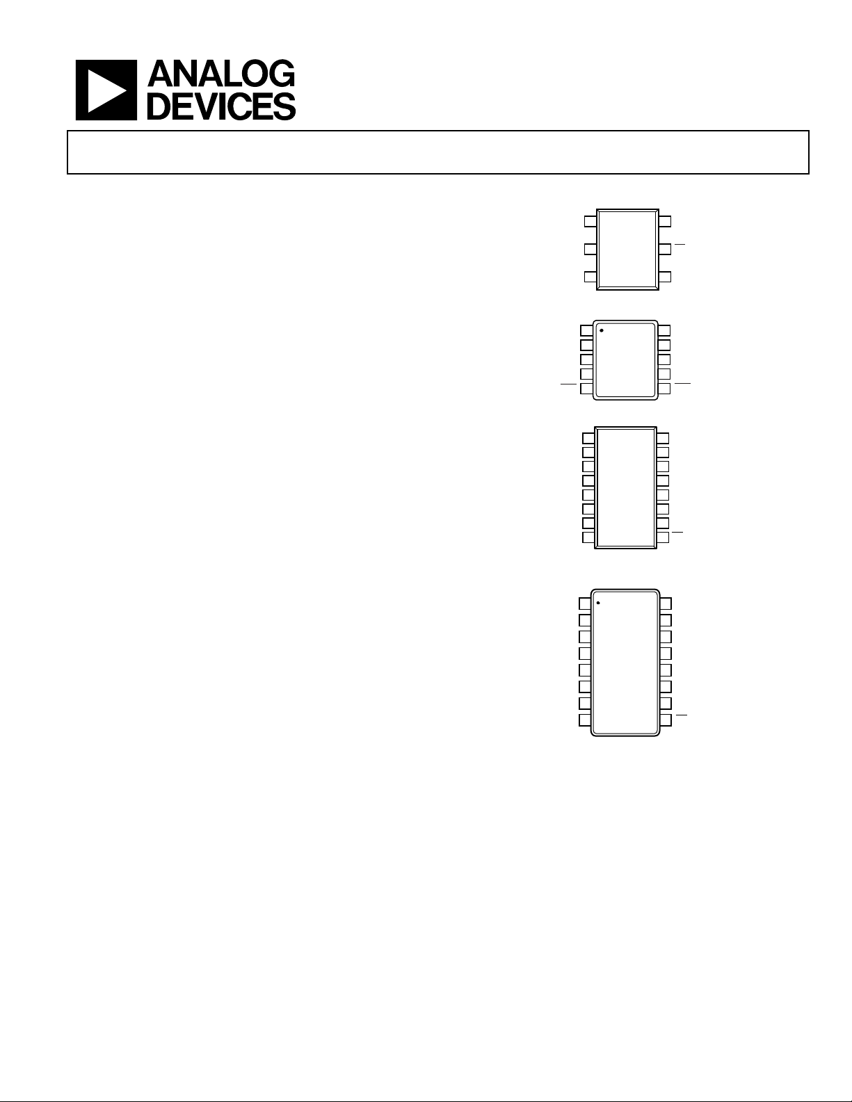
PIN CONFIGURATIONS
1
UT A
AD
V–
2
TOP VIEW
(Not to Scale)
+IN A
3
Figure 1. 6-Lead SOT-23 (RJ Suffix)
OUT A
1
–IN A
2
AD
3
+IN A
SDA
V–
TOP VIEW
(Not to Scale)
4
5
Figure 2. 10-Lead MSOP (RM Suffix)
1
OUT A
2
–IN A
+IN A
3
AD
4
V+
TOP VIEW
+IN B
–IN B
OUT B
(Not to Scale)
5 12
6 11
7 10
8 9
NC
NC = NO CONNECT
Figure 3. 16-Lead Narrow SOIC (R Suffix)
1
OUT A
2
–IN A
3
+IN A
+IN B
–IN B
OUT B
NC
AD
TOP VIEW
4
V+
(Not to Scale)
5
6
7
8
NC = NO CONNECT
Figure 4. 16-Lead TSSOP (RU Suffix)
The AD8591, AD8592, and AD8594 are specified over the
industrial temperature range (−40°C to +85°C). The AD8591,
single, is available in the tiny 6-lead SOT-23 package. The AD8592,
dual, is available in the 10-lead surface-mount MSOP package. The
AD8594, quad, is available in 16-lead narrow SOIC and 16-lead
TSSOP packages.
8591
8592
8594
8594
10
16
15
14
13
6
5
4
9
8
7
6
16
15
14
13
12
11
10
9
V+
SD
–IN A
V+
OUT B
–IN B
+IN B
SDB
OUT D
–IN D
+IN D
V–
+IN C
–IN C
OUT C
SD
OUT D
–IN D
+IN D
V–
+IN C
–IN C
OUT C
SD
1106-001
1106-002
01106-003
01106-004
Rev. B
Information furnished by Analog Devices is believed to be accurate and reliable. However, no
responsibility is assumed by Analog Devices for its use, nor for any infringements of patents or other
rights of third parties that may result from its use. Specifications subject to change without notice. No
license is granted by implication or otherwise under any patent or patent rights of Analog Devices.
Trademarks and registered trademarks are the property of their respective owners.
One Technology Way, P.O. Box 9106, Norwood, MA 02062-9106, U.S.A.
Tel: 781.329.4700 www.analog.com
Fax: 781.461.3113 ©2009 Analog Devices, Inc. All rights reserved.

AD8591/AD8592/AD8594
TABLE OF CONTENTS
Features .............................................................................................. 1
Applications ....................................................................................... 1
General Description ......................................................................... 1
Pin Configurations ........................................................................... 1
Revision History ............................................................................... 2
Specifications ..................................................................................... 3
Electrical Characteristics ............................................................. 3
Absolute Maximum Ratings ............................................................ 5
Thermal Resistance ...................................................................... 5
ESD Caution .................................................................................. 5
Typical Performance Characteristics ............................................. 6
Theory of Operation ...................................................................... 11
Input Voltage Protection............................................................ 11
Output Phase Reversal ............................................................... 11
Output Short-Circuit Protection .............................................. 11
Power Dissipation....................................................................... 11
Capacitive Loading ..................................................................... 12
PC98-Compliant Headphone/Speaker Amplifier .................. 12
A Combined Microphone and Speaker Amplifier for
Cellphone and Portable Headsets ............................................ 13
An Inexpensive Sample-and-Hold Circuit ............................. 13
Direct Access Arrangement for PCMCIA Modems
(Telephone Line Interface) ........................................................ 14
Single-Supply Differential Line Driver .................................... 14
Outline Dimensions ....................................................................... 15
Ordering Guide .......................................................................... 16
REVISION HISTORY
1/09—Rev. A to Rev. B
Updated Format .................................................................. Universal
Changes to Table 1 ............................................................................ 3
Changes to Table 2 ............................................................................ 4
Deleted Spice Model for AD8591/AD8592/AD8594 Amplifiers
Sections ............................................................................................ 12
Changes to PC98-Compliant Headphone/Speaker Amplifier
Section and Figure 38 ..................................................................... 12
Changes to Figure 39 ...................................................................... 13
Changes to Figure 42 and Figure 43 ............................................. 14
Updated Outline Dimensions ....................................................... 15
Changes to Ordering Guide .......................................................... 16
Rev. B | Page 2 of 16

AD8591/AD8592/AD8594
SPECIFICATIONS
ELECTRICAL CHARACTERISTICS
VS = 2.7 V, VCM = 1.35 V, TA = 25°C, unless otherwise noted.
Table 1.
Parameter Symbol Test Conditions Min Typ Max Unit
INPUT CHARACTERISTICS
Offset Voltage VOS 25 mV
−40°C < TA < +85°C 30 mV
Input Bias Current IB 5 50 pA
−40°C < TA < +85°C 60 pA
Input Offset Current IOS 1 25 pA
−40°C < TA < +85°C 30 pA
Input Voltage Range 0 2.7 V
Common-Mode Rejection Ratio CMRR VCM = 0 V to 2.7 V 38 45 dB
Large Signal Voltage Gain AVO R
Offset Voltage Drift ΔVOS/ΔT −40°C < TA < +85°C 20 μV/°C
Bias Current Drift ΔIB/ΔT −40°C < TA < +85°C 50 fA/°C
Offset Current Drift ΔIOS/ΔT −40°C < TA < +85°C 20 fA/°C
OUTPUT CHARACTERISTICS
Output Voltage High VOH I
−40°C to +85°C 2.5 V
Output Voltage Low VOL I
−40°C to +85°C 125 mV
Output Current I
Open-Loop Impedance Z
±250 mA
OUT
f = 1 MHz, AV = 1 60 Ω
OUT
POWER SUPPLY
Power Supply Rejection Ratio PSRR VS = 2.5 V to 6 V 45 55 dB
Supply Current per Amplifier ISY V
−40°C < TA < +85°C 1.25 mA
Supply Current Shutdown Mode ISD All amplifiers shut down 0.1 1 μA
−40°C < TA < +85°C 1 μA
I
I
Amplifier 1 shut down (AD8592) 1.4 mA
SD1
Amplifier 2 shut down (AD8592) 1.4 mA
SD2
SHUTDOWN INPUTS
Logic High Voltage V
Logic Low Voltage V
−40°C < TA < +85°C 1.6 V
INH
−40°C < TA < +85°C 0.5 V
INL
Logic Input Current IIN −40°C < TA < +85°C 1 μA
DYNAMIC PERFORMANCE
Slew Rate SR RL = 2 kΩ 3.5 V/μs
Settling Time tS To 0.01% 1.4 μs
Gain Bandwidth Product GBP 2.2 MHz
Phase Margin Φo 67 Degrees
Channel Separation CS f = 1 kHz, RL = 2 kΩ 65 dB
NOISE PERFORMANCE
Voltage Noise Density en f = 1 kHz 45 nV/√Hz
f = 10 kHz 30 nV/√Hz
Current Noise Density in f = 1 kHz 0.05 pA/√Hz
= 2 kΩ, VO = 0.3 V to 2.4 V 25 V/mV
L
= 10 mA 2.55 2.61 V
L
= 10 mA 60 100 mV
L
= 0 V 1 mA
O
Rev. B | Page 3 of 16

AD8591/AD8592/AD8594
VS = 5.0 V, VCM = 2.5 V, TA = 25°C, unless otherwise noted.
Table 2.
Parameter Symbol Test Conditions Min Typ Max Unit
INPUT CHARACTERISTICS
Offset Voltage VOS 2 25 mV
−40°C < TA < +85°C 30 mV
Input Bias Current IB 5 50 pA
−40°C < TA < +85°C 60 pA
Input Offset Current IOS 1 25 pA
−40°C < TA < +85°C 30 pA
Input Voltage Range 0 5 V
Common-Mode Rejection Ratio CMRR VCM = 0 V to 5 V 38 47 dB
Large Signal Voltage Gain AVO R
Offset Voltage Drift ΔVOS/ΔT −40°C < TA < +85°C 20 μV/°C
Bias Current Drift ΔIB/ΔT −40°C < TA < +85°C 50 fA/°C
Offset Current Drift ΔIOS/ΔT −40°C < TA < +85°C 20 fA/°C
OUTPUT CHARACTERISTICS
Output Voltage High VOH I
−40°C to +85°C 4.85 V
Output Voltage Low VOL I
−40°C to +85°C 125 mV
Output Current I
Open-Loop Impedance Z
±250 mA
OUT
f = 1 MHz, AV = 1 40 Ω
OUT
POWER SUPPLY
Power Supply Rejection Ratio PSRR VS = 2.5 V to 6 V 45 55 dB
Supply Current per Amplifier ISY V
−40°C < TA < +85°C 1.75 mA
Supply Current Shutdown Mode ISD All amplifiers shut down 0.1 1 μA
−40°C < TA < +85°C 1 μA
I
I
Amplifier 1 shut down (AD8592) 1.6 mA
SD1
Amplifier 2 shut down (AD8592) 1.6 mA
SD2
SHUTDOWN INPUTS
Logic High Voltage V
Logic Low Voltage V
−40°C < TA < +85°C 2.4 V
INH
−40°C < TA < +85°C 0.8 V
INL
Logic Input Current IIN −40°C < TA < +85°C 1 μA
DYNAMIC PERFORMANCE
Slew Rate SR RL = 2 kΩ 5 V/μs
Full Power Bandwidth BWP 1% distortion 325 kHz
Settling Time tS To 0.01% 1.6 μs
Gain Bandwidth Product GBP 3 MHz
Phase Margin Φo 70 Degrees
Channel Separation CS f = 1 kHz, RL = 10 kΩ 65 dB
NOISE PERFORMANCE
Voltage Noise Density en f = 1 kHz 45 nV/√Hz
f = 10 kHz 30 nV/√Hz
Current Noise Density in f = 1 kHz 0.05 pA/√Hz
= 2 kΩ, VO = 0.5 V to 4.5 V 15 30 V/mV
L
= 10 mA 4.9 4.94 V
L
= 10 mA 50 100 mV
L
= 0 V 1.25 mA
O
Rev. B | Page 4 of 16
AD8591/AD8592/AD8594
ABSOLUTE MAXIMUM RATINGS
Table 3.
Parameter Rating
Supply Voltage 6 V
Input Voltage GND to VS
Differential Input Voltage ±6 V
Output Short-Circuit Duration to GND1 Observe Derating Curves
Storage Temperature Range −65°C to +150°C
Operating Temperature Range −40°C to +85°C
Junction Temperature Range −65°C to +150°C
Lead Temperature (Soldering, 60 sec) 300°C
1
For supplies less than ±5 V, the differential input voltage is limited to the
supplies.
Stresses above those listed under Absolute Maximum Ratings
may cause permanent damage to the device. This is a stress
rating only; functional operation of the device at these or any
other conditions above those listed in the operational sections
of this specification is not implied. Exposure to absolute
maximum rating conditions for extended periods may affect
device reliability.
THERMAL RESISTANCE
θJA is specified for the worst-case conditions, that is, a device
soldered in a circuit board for surface-mount packages.
Table 4.
Package Type θ
6-Lead SOT-23 (RJ) 230 92 °C/W
10-Lead MSOP (RM) 200 44 °C/W
16-Lead SOIC (R) 120 36 °C/W
16-Lead TSSOP (RU) 180 35 °C/W
θJC Unit
JA
ESD CAUTION
Rev. B | Page 5 of 16
AD8591/AD8592/AD8594
–
TYPICAL PERFORMANCE CHARACTERISTICS
1k
VS = 2.7V
T
= 25°C
A
0.8
0.7
TA = 25°C
100
10
ΔOUTPUT VOL TAGE (mV)
1
0.1
SOURCE
LOAD CURRENT (mA)
SINK
Figure 5. Output Voltage to Supply Rail vs. Load Current
10k
VS = 5V
T
= 25°C
A
1k
100
SOURCE
10
ΔOUTPUT VOLTAGE (mV)
1
SINK
0.6
0.5
0.4
0.3
0.2
SUPPLY CURRENT/ AMPLIFIER (mA)
0.1
0
1k0.01 0. 1 1 10 100
01106-005
0.75 1.25 1.75 2.25 2.75 3.00
SUPPLY VOLTAGE (±V)
01106-008
Figure 8. Supply Current per Amplifier vs. Supply Voltage
2
V
= 5V
S
V
= 2.5V
CM
–3
–4
–5
–6
INPUT OFFSET VOLTAGE (mV)
–7
0.1
LOAD CURRENT (mA)
Figure 6. Output Voltage to Supply Rail vs. Load Current
0.90
0.85
0.80
0.75
0.70
0.65
0.60
SUPPLY CURRENT/ AMPLIFI ER (mA)
0.55
0.50
–40 –20 1000 20406080
VS = 5V
VS = 2.7V
TEMPERATURE ( °C)
Figure 7. Supply Current per Amplifier vs. Temperature
–8
1k0.01 0.1 1 10 100
1106-006
–50 –35 85
5
–15
TEMPERATURE ( °C)
25 45 65
01106-009
Figure 9. Input Offset Voltage vs. Temperature
8
VS = 2.7V, 5V
= VS/2
V
CM
7
6
5
4
INPUT BIAS CURRENT (pA)
3
2
–50 –35 855–15 25 45 65
01106-007
TEMPERATURE ( °C)
01106-010
Figure 10. Input Bias Current vs. Temperature
Rev. B | Page 6 of 16
AD8591/AD8592/AD8594
4
= 2.7V, 5V
V
S
V
= VS/2
CM
3
2
1
0
INPUT OFFSET CURRENT (pA)
–1
80
60
40
20
0
GAIN (dB)
VS = 5V
R
= NO LOAD
L
T
= 25°C
A
45
90
135
180
PHASE SHIF T (Degrees)
–2
–50 –35 855–15 25 45 65
TEMPERATURE ( °C)
Figure 11. Input Offset Current vs. Temperature
8
VS = 5V
T
= 25°C
A
7
6
5
4
3
INPUT BIAS CURRENT (pA)
2
1
COMMON-MODE VOLTAGE (V)
Figure 12. Input Bias Current vs. Common-Mode Voltage
80
60
40
20
VS = 2.7V
R
= NO LOAD
L
T
= 25°C
A
45
90
135
1k 10k 100k 1M 10M 100M
01106-011
FREQUENCY (Hz)
01106-014
Figure 14. Open-Loop Gain and Phase vs. Frequency
5
4
3
2
OUTPUT SWING (V p-p)
1
510 234
1106-012
0
1k 10k 100k 1M 10M
FREQUENCY (Hz)
VS = 2.7V
R
= 2kΩ
L
T
= 25°C
A
VIN = 2.5V p-p
01106-016
Figure 15. Closed-Loop Output Voltage Swing vs. Frequency
5
4
3
VS = 5V
R
= 2kΩ
L
T
= 25°C
A
VIN = 2.5V p-p
0
GAIN (dB)
1k 10k 100k 1M 10M 100M
FREQUENCY (Hz)
Figure 13. Open-Loop Gain and Phase vs. Frequency
180
PHASE SHIFT (Degrees)
01106-013
Rev. B | Page 7 of 16
2
OUTPUT SWING (V p-p)
1
0
1k 10k 100k 1M 10M
FREQUENCY (Hz)
Figure 16. Closed-Loop Output Voltage Swing vs. Frequency
01106-017

AD8591/AD8592/AD8594
200
VS = 5V
T
= 25°C
A
180
160
140
Ω)
120
100
80
IMPEDANCE (
60
40
20
0
1k 10k 100k 1M 10M 100M
AV = 10
AV = 1
FREQUENCY (Hz)
Figure 17. Closed-Loop Output Impedance vs. Frequency
110
100
90
VS = 5V
T
= 25°C
A
01106-018
140
120
100
80
60
40
PSRR (dB)
20
0
–20
–40
–60
–PSRR
+PSRR
100 1k 10k 100k 1M 10M
FREQUENCY (Hz)
Figure 20. Power Supply Rejection Ratio vs. Frequency
60
VS = 2.5V
R
= 2kΩ
L
T
= 25°C
A
50
40
+OS
VS = 5V
T
= 25°C
A
–OS
01106-021
80
CMRR (dB)
70
60
50
1k 10k 100k 1M 10M
FREQUENCY (Hz)
Figure 18. Common-Mode Rejection Ratio vs. Frequency
140
120
100
80
60
40
PSRR (dB)
20
–20
–40
–60
+PSRR
–PSRR
0
100 1k 10k 100k 1M 10M
FREQUENCY (Hz)
Figure 19. Power Supply Rejection Ratio vs. Frequency
VS = 2.5V
T
= 25°C
A
30
20
SMALL SIGNAL OVERSHOOT (%)
10
0
10 100 1k 10k
01106-019
CAPACITANCE (pF )
01106-022
Figure 21. Small Signal Overshoot vs. Load Capacitance
60
VS = 5V
R
= 2kΩ
L
T
= 25°C
A
50
40
30
20
SMALL SIGNAL OVERSHOOT (%)
10
0
10 100 1k 10k
01106-020
CAPACITANCE (pF )
–OS
+OS
01106-023
Figure 22. Small Signal Overshoot vs. Load Capacitance
Rev. B | Page 8 of 16

AD8591/AD8592/AD8594
V
V
VS = ±2.5V
A
= +1
V
R
= 2kΩ
100
90
L
T
A
= 25°C
0V
20mV/DI
Figure 23. Small Signal Transient Response
VS = ±1.35V
V
= ±50mV
IN
A
= +1
V
R
= 2kΩ
L
C
= 300pF
L
T
= 25°C
A
500 ns/DIV
10
0
500mV 500ns
01106-024
01106-027
Figure 26. Large Signal Transient Response
10µs1V
100
90
0V
20mV/DI
Figure 24. Small Signal Transient Response
100
90
VS = ±2.5V
V
= ±50mV
IN
A
= +1
V
R
= 2kΩ
L
C
= 300pF
L
T
= 25°C
A
500 ns/DIV
VS = ±1.35V
A
= +1
V
R
= 2kΩ
L
T
= 25°C
A
10
0
1V
01106-025
VS = ±2.5V
A
= +1
V
T
= +25°C
A
01106-028
Figure 27. No Phase Reversal
1
√Hz)
VS = 5V
T
= 25°C
A
0.1
10
0
500mV 500ns
Figure 25. Large Signal Transient Response
01106-026
CURRENT NOISE DE NSITY (pA/
0.01
10 100 1k 10k 100k
FREQUENCY (Hz)
Figure 28. Current Noise Density vs. Frequency
01106-029
Rev. B | Page 9 of 16

AD8591/AD8592/AD8594
V
600
500
400
300
200
QUANTITY (Amplifi ers)
100
0
–12–14 6–10
–8 –6 –4 –2 0 2 4
INPUT OFFSET VOLTAGE (mV)
VS = 2.7V
V
= 1.35V
CM
T
= 25°C
A
01106-032
Figure 31. Input Offset Voltage Distribution
600
500
400
300
200
QUANTITY ( Amplifiers)
100
VS = 5V
V
= 2.5V
CM
T
= 25°C
A
100
90
100µV/DIV
10
0
MARKER 41µV/√Hz
Figure 29. Voltage Noise Density vs. Frequency
100
90
200µV/DI
10
0
VS = 5V
A
= +1000
V
T
= 25°C
A
FREQUENCY = 1kHz
VS = 5V
= +1000
A
V
= 25°C
T
A
FREQUENCY = 10kHz
01106-030
MARKER 25.9
µV/√Hz
Figure 30. Voltage Noise Density vs. Frequency
01106-031
0
–12–14 6–10
–8 –6 –4 –2 0 2 4
INPUT OFFSET VOLTAGE (mV)
Figure 32. Input Offset Voltage Distribution
1106-033
Rev. B | Page 10 of 16
AD8591/AD8592/AD8594
V
V
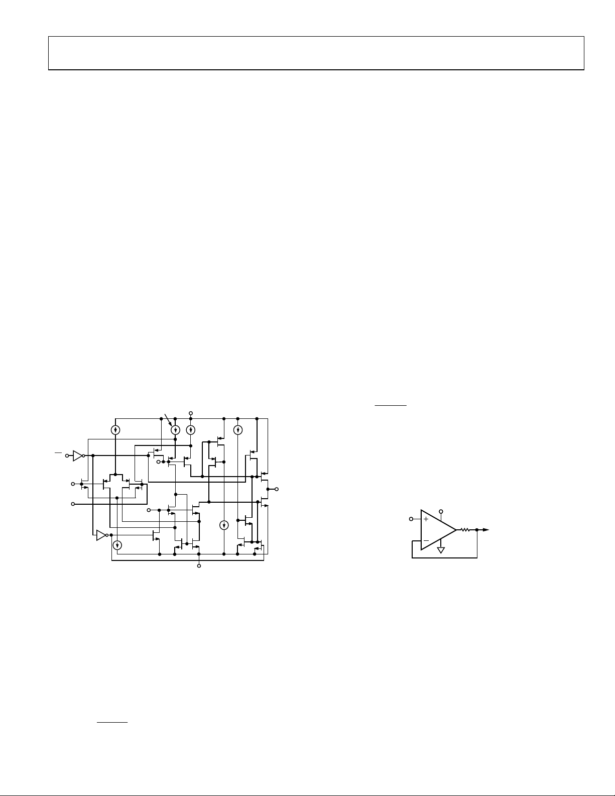
THEORY OF OPERATION
The AD859x amplifiers are CMOS, high output drive, rail-torail input and output single-supply amplifiers designed for low
cost and high output current drive. The parts include a power
saving shutdown function that makes the AD8591/AD8592/
AD8594 op amps ideal for portable multimedia and
telecommunications applications.
Figure 33 shows the simplified schematic for the AD8591/AD8592/
AD8594 amplifiers. Two input differential pairs, consisting of
an n-channel pair (M1, M2) and a p-channel pair (M3, M4),
provide a rail-to-rail input common-mode range. The outputs of
the input differential pairs are combined in a compound foldedcascode stage that drives the input to a second differential pair
gain stage. The outputs of the second gain stage provide the gate
voltage drive to the rail-to-rail output stage.
The rail-to-rail output stage consists of M15 and M16, which
are configured in a complementary common source configuration.
As with any rail-to-rail output amplifier, the gain of the output
stage, and thus the open-loop gain of the amplifier, is dependent
on the load resistance. In addition, the maximum output voltage
swing is directly proportional to the load current. The difference
between the maximum output voltage to the supply rails, known as
the dropout voltage, is determined by the on-channel resistance
of the AD8591/AD8592/AD8594 output transistors. The output
dropout voltage is given in Figure 5 and Figure 6.
100µA
50µA
INV
SD
M3
M1
IN–
IN+
INV
*ALL CURRENT SOURCES GO TO 0µA IN SHUTDOWN MODE.
M4
*
50µA
M337
M2
V
B3
M340
V
B2
Figure 33. Simplified Schematic
+
**
*
100µA
M5
M8
M6
M7 M10
M9
V–
20µA
M12
M11
M13
*
20µA
M30
M15
OUT
M16
M14
*
M31
INPUT VOLTAGE PROTECTION
Although not shown in the simplified schematic, ESD protection
diodes are connected from each input to each power supply rail.
These diodes are normally reverse-biased, but turn on if either
input voltage exceeds either supply rail by more than 0.6 V. If this
condition occurs, limit the input current to less than ±5 mA.
This is done by placing a resistor in series with the input(s).
The minimum resistor value should be
V
,MAXIN
R ≥
IN
(1)
mA5
01106-034
OUTPUT PHASE REVERSAL
The AD8591/AD8592/AD8594 are immune to output voltage
phase reversal with an input voltage within the supply voltages
of the device. However, if either of the inputs of the device exceeds
0.6 V outside of the supply rails, the output could exhibit phase
reversal. This is due to the ESD protection diodes becoming
forward-biased, thus causing the polarity of the input terminals
of the device to switch.
The technique recommended in the Input Voltage Protection
section should be applied in applications where the possibility
of input voltages exceeding the supply voltages exists.
OUTPUT SHORT-CIRCUIT PROTECTION
To achieve high output current drive and rail-to-rail performance,
the outputs of the AD859x family do not have internal shortcircuit protection circuitry. Although these amplifiers are
designed to sink or source as much as 250 mA of output current,
shorting the output directly to the positive supply could damage or
destroy the device. To protect the output stage, limit the maximum
output current to ±250 mA.
By placing a resistor in series with the output of the amplifier,
as shown in Figure 34, the output current can be limited. The
minimum value for R
V
R ≥ (2)
SY
X
For a 5 V single-supply application, R
Because R
is inside the feedback loop, V
X
trade-off in using R
swing under heavy output current loads. R
effective output impedance of the amplifier to R
is
X
mA250
should be at least 20 Ω.
X
is not affected. The
OUT
is a slight reduction in output voltage
X
also increases the
X
+ RX, where RO
O
is the output impedance of the device.
+5
R
V
IN
AD8592
Figure 34. Output Short-Circuit Protection
20Ω
X
V
OUT
01106-035
POWER DISSIPATION
Although the AD859x amplifiers are able to provide load
currents of up to 250 mA, proper attention should be given to
not exceeding the maximum junction temperature for the device.
The junction temperature equation is
T
= P
× θJA + TA (3)
J
DISS
where:
T
is the AD859x junction temperature.
J
P
is the AD859x power dissipation.
DISS
θ
is the AD859x junction-to-ambient thermal resistance of the
JA
package.
T
is the ambient temperature of the circuit.
A
Rev. B | Page 11 of 16

AD8591/AD8592/AD8594
4
V
R
In any application, the absolute maximum junction temperature
must be limited to 150°C. If the junction temperature is exceeded,
the device could suffer premature failure. If the output voltage
and output current are in phase, for example, with a purely resistive
load, the power dissipated by the AD859x can be found as
P
= I
DISS
× (VSY − V
LOAD
) (4)
OUT
where:
I
is the AD859x output load current.
LOAD
V
is the AD859x supply voltage.
SY
V
is the output voltage.
OUT
By calculating the power dissipation of the device and using the
thermal resistance value for a given package type, the maximum
allowable ambient temperature for an application can be found
using Equation 3.
CAPACITIVE LOADING
The AD859x exhibits excellent capacitive load driving capabilities
and can drive to 10 nF directly. Although the device is stable
with large capacitive loads, there is a decrease in amplifier
bandwidth as the capacitive load increases. Figure 35 shows
a graph of the AD8592 unity-gain bandwidth under various
capacitive loads.
4.0
3.5
3.0
2.5
2.0
1.5
BANDWIDTH (MHz)
1.0
0.5
0
0.01 0.1
CAPACITIVE L OAD (nF)
110
Figure 35. Unity-Gain Bandwidth vs. Capacitive Load
When driving heavy capacitive loads directly from the AD859x
output, a snubber network can be used to improve the transient
response. This network consists of a series RC connected from
the output of the amplifier to ground, placing it in parallel with
the capacitive load. The configuration is shown in Figure 36.
Although this network does not increase the bandwidth of the
amplifier, it significantly reduces the amount of overshoot, as
shown in Figure 37.
+5V
AD8592
V
IN
100mV p-p
Figure 36. Configuration for Snubber N etwork to Compensate for Capacitive Loads
R
S
5Ω
C
S
1µF
C
L
47nF
VS = ±2.5V
= 1kΩ
R
L
= 25°C
T
A
V
OUT
100
01106-036
01106-037
7nF LOAD
ONLY
SNUBBER
IN CIRCUIT
Figure 37. Snubber Network Reduces Overshoot and Ringing
The optimum values for the snubber network should be
determined empirically based on the size of the capacitive load.
Tabl e 5 shows a few sample snubber network values for a given
load capacitance.
Table 5. Snubber Networks for Large Capacitive Loads
Load Capacitance, CL (nF)
0.47 300 0.1
4.7 30 1
47 5 1
PC98-COMPLIANT HEADPHONE/SPEAKER AMPLIFIER
Because of its high output current performance and shutdown
feature, the AD8592 makes an excellent amplifier for driving an
audio output jack in a computer application. Figure 38 shows
how the AD8592 can be interfaced with an AC’97 codec to
drive headphones or speakers.
AV
DD1
AV
DD2
LINE_OUT_L
AD1881A*
(AC’97)
LINE_OUT_
AV
SS1
*ADDITIONALPINS OMITTED FOR CLARITY.
Figure 38. PC98-Compliant Headphone/Line Out Amplifier
50mV
50mV 10µ s
Caused by Driving Heavy Capacitive Loads
Snubber Network
RS (Ω) CS (μF)
+5
25
38
35
36
26
+5V
10
2
U1-A
1
4
3
5
100kΩ
6
7
U1-B
9
8
C1
100µF
R2
C2
100µF
2kΩ
R3
2kΩ
+5V
R1
U1 = AD8592
20Ω
R5
20Ω
01106-038
R4
NC
01106-039
Rev. B | Page 12 of 16

AD8591/AD8592/AD8594
V
R
A
V
When headphones are plugged into the jack, the normalizing
contacts disconnect from the audio contacts. This allows the
voltage to the AD8592 shutdown pins to be pulled to 5 V,
activating the amplifiers. With no plug in the output jack, the
shutdown voltage is pulled to 100 mV through the R1 and R3 + R5
voltage divider. This powers the AD8592 down when it is not
needed, saving current from the power supply or battery.
If gain is required from the output amplifier, add four additional
resistors, as shown in Figure 39. The gain of the AD8592 can
be set as
R
(5)
=
A
V
67R
+5
25
AV
DD1
38
AV
DD2
VREF
AV
SS1
35
R6
10kΩ
27
R6
10kΩ
36
26
LINE_OUT_L
AD1881A*
(AC’97)
LINE_OUT_
*ADDITIONAL PINS OMI TTED FO R CLARITY.
R7
10kΩ
+5V
10
2
U1-A
1
5
6
U1-B
10kΩ
R7
R6
R7
4
100kΩ
9
U1 = AD8592
3
7
8
AV = = 6dB WITH VALUES SHOWN
C1
100µF
+5V
R1
100µF
20Ω
R2
2kΩ
C2
20Ω
R3
2kΩ
R4
NC
R5
Figure 39. PC98-Compliant Headphone/Line Out Amplifier with Gain
Input coupling capacitors are not required for either circuit
because the reference voltage is supplied from the AD1881A.
R4 and R5 help protect the AD8592 output in case the output
jack or headphone wires accidentally are shorted to ground. The
output coupling capacitors, C1 and C2, block dc current from the
headphones and create a high-pass filter with a corner frequency of
f+π=
where R
−
3
dB
is the resistance of the headphones.
L
1
()
412
(6)
RRC
L
01106-040
A COMBINED MICROPHONE AND SPEAKER AMPLIFIER FOR CELLPHONE AND PORTABLE HEADSETS
The dual amplifiers in the AD8592 make an efficient design for
interfacing with a headset containing a microphone and speaker.
Figure 40 demonstrates a simple method for constructing an
interface to a codec.
R3
100kΩ
+5V
10
2
U1-A
1
4
3
5
6
7
U1-B
9
8
R5
10kΩ
(OPTIONAL)
R4
10kΩ
R6
10kΩ
TO
CODEC
V
REF
FROM CODEC
FROM CODEC
MONO OUT
(OR LEFT OUT)
(RIGHT OUT)
MICROPHONE
ND SPEAKE R
JACK
+5V
R1
2.2kΩ
NC
R7
1kΩ
U1 = AD8592
C1
0.1µF
100kΩ
C2
10µF
R2
10kΩ
+5V
R8
Figure 40. Speaker/Microphone Headset Amplifier Circuit
U1-A is used as a microphone preamplifier, where the gain of
the preamplifier is set as R3/R2. R1 is used to bias an electret
microphone, and C1 blocks any dc voltages from the amplifier.
U1-B is the speaker amplifier, and its gain is set at R5/R4. To
sum a stereo output, add R6, equal in value to R4.
Using the same principle described in the PC98-Compliant
Headphone/Speaker Amplifier section, the normalizing contact
on the microphone/speaker jack can be used to put the AD8592
into shutdown when the headset is not plugged in. The AD8592
shutdown inputs can also be controlled with TTL- or CMOScompatible logic, allowing microphone or speaker muting, if
desired.
AN INEXPENSIVE SAMPLE-AND-HOLD CIRCUIT
The independent shutdown control of each amplifier in the
AD8592 allows a degree of flexibility in circuit design. One
particular application for which this feature is useful is in
designing a sample-and-hold circuit for data acquisition. Figure 41
shows a schematic of a simple, yet extremely effective, sampleand-hold circuit using a single AD8592 and one capacitor.
C1
1nF
8
U1-B
6
7
U1 = AD8592
+5V
9
SAMPLE
AND HOLD
OUTPUT
+5V
2
10
U1-A
IN
3
SAMPLE
CLOCK
1
4
5
Figure 41. An Efficient Sample-and-Hold Circuit
01106-041
1106-042
Rev. B | Page 13 of 16
AD8591/AD8592/AD8594
R
The U1-A amplifier is configured as a unity-gain buffer driving
a 1 nF capacitor. The input signal is connected to the noninverting
input, and the sample clock controls the shutdown for that
amplifier. When the sample clock is high, the U1-A amplifier is
active and the output follows V
. When the sample clock goes
IN
low, U1-A shuts down with the output of the amplifier going to
a high impedance state, holding the voltage on the C1 capacitor.
The U1-B amplifier is used as a unity-gain buffer to prevent
loading on C1. Because of the low input bias current of the U1-B
CMOS input stage and the high impedance state of the U1-A
output in shutdown, there is little voltage droop from C1 during
the hold period. This circuit can be used with sample frequencies as
high as 500 kHz and as low as 1 Hz. By increasing the C1 value,
lower voltage droop is achieved for very low sample rates.
DIRECT ACCESS ARRANGEMENT FOR PCMCIA MODEMS (TELEPHONE LINE INTERFACE)
Figure 42 illustrates a 5 V transmit/receive telephone line
interface for 600 Ω systems. It allows full duplex transmission
of signals on a transformer-coupled 600 Ω line in a differential
manner. Amplifier A1 provides gain that can be adjusted to
meet the modem output drive requirements. Both A1 and A2
are configured to apply the largest possible signal on a single
supply to the transformer. Because of the high output current
drive and low dropout voltages of the AD8594, the largest signal
available on a single 5 V supply is approximately 4.5 V p-p into
a 600 Ω transmission system. Amplifier A3 is configured as a
difference amplifier for two reasons. It prevents the transmit
signal from interfering with the receive signal, and it extracts
the receive signal from the transmission line for amplification
by A4. The gain of A4 can be adjusted in the same manner as
the gain of A1 to meet the input signal requirements of the
modem. Standard resistor values permit the use of single
inline package (SIP) format resistor arrays. Couple this with
the 16-lead TSSOP or SOIC footprint of the AD8594, and this
circuit offers a compact, cost-effective solution.
P1
Tx GAIN
ADJUST
TO TELEPHONE
LINE
1:1
Z
O
600Ω
T1
MIDCOM
671-8005
A1, A2 = 1/4 AD8594
A3, A4 = 1/4 AD8594
6.2V
6.2V
R11
10kΩ
360Ω
R9
10kΩ
R12
10kΩ
R3
R5
10kΩ
R6
10kΩ
R10
10kΩ
9
11
A3
12
Figure 42. Single-Supply Direct Access Arrangement for PCMCIA Modems
10
2kΩ
1
7
9
9.09kΩ
A1
9
A2
R13
10kΩ
R2
2
3
6
5
14.3kΩ
15
14
R14
10kΩ
9
A4
R1
Rx GAIN
ADJUST
2kΩ
0.1µF
P2
16
C1
10µF
SHUTDOWN
+5V
C2
0.1µF
TRANSMIT
TxA
R7
10kΩ
R8
10kΩ
RECEIVE
RxA
1106-043
SINGLE-SUPPLY DIFFERENTIAL LINE DRIVER
Figure 43 shows a single-supply differential line driver circuit
that can drive a 600 Ω load with less than 0.7% distortion from
20 Hz to 15 kHz with an input signal of 4 V p-p and a single 5 V
supply. The design uses an AD8594 to mimic the performance
of a fully balanced transformer-based solution. However, this
design occupies much less board space, while maintaining low
distortion, and can operate down to dc. Like the transformer-based
design, either output can be shorted to ground for unbalanced
line driver applications without changing the circuit gain of 1.
3
10kΩ
2
C1
22µF
V
IN
A1, A2 = 1/2 AD8592
GAIN =
SET: R7,R10, R11 = R2
SET: R6,R12, R13 = R3
A1
3
R3
R2
+5V
10
10kΩ
4
10kΩ
10kΩ
R1
R10
2
1
A2
3
R2
R7
10kΩ
+5V
R11
10kΩ
8
7
10
A1
9
4
R12
10kΩ
9
A2
R13
10kΩ
1
10kΩ
8
7
100kΩ
R5
50Ω
R6
+5V
R8
100kΩ
C2
R9
1µF
R14
50Ω
Figure 43. Low Noise, Single-Supply Differential Line Driver
R8 and R9 set up the common-mode output voltage equal to
half of the supply voltage. C1 is used to couple the input signal
and can be omitted if the dc voltage of the input is equal to half
of the supply voltage.
The circuit can also be configured to provide additional gain, if
desired. The gain of the circuit is
V
A
V
R
OUT
== (7)
V
23R
IN
where:
V
= VO1 − VO2
OUT
R2 = R7 = R10 = R11
R3 = R6 = R12 = R1
C3
47µF
600Ω
C4
47µF
V
O1
R
L
V
O2
1106-044
Rev. B | Page 14 of 16
AD8591/AD8592/AD8594
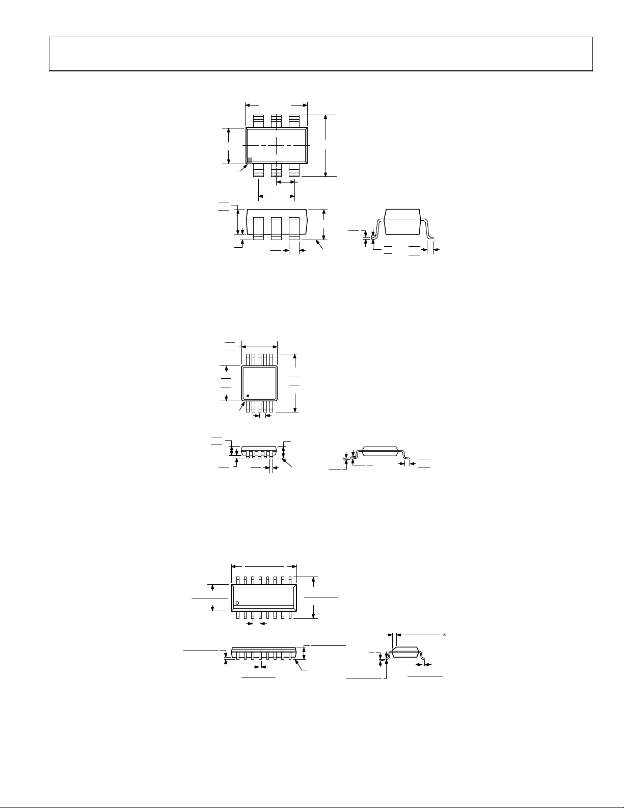
OUTLINE DIMENSIONS
2.90 BSC
4526
1.60 BSC
PIN 1
INDICATOR
1.30
1.15
0.90
0.15 MAX
1 3
1.90
BSC
0.50
0.30
COMPLIANT TO JEDEC STANDARDS MO-178-AB
2.80 BSC
0.95 BSC
1.45 MAX
SEATING
PLANE
0.22
0.08
Figure 44. 6-Lead Small Outline Transistor Package [SOT-23]
(RJ-6)
Dimensions shown in millimeters
3.10
3.00
2.90
6
0.95
0.85
0.75
3.10
3.00
2.90
0.15
0.05
PIN 1
10
1
0.50 BSC
0.33
0.17
COPLANARITY
0.10
COMPLIANT TO JEDEC STANDARDS MO-187-BA
5.15
4.90
4.65
5
1.10 MAX
SEATING
PLANE
0.23
0.08
Figure 45. 10-Lead Mini Small Outline Package [MSOP]
(RM-10)
Dimensions shown in millimeters
10.00 (0.3937)
9.80 (0.3858)
10°
0.60
4°
0.45
0°
0.30
8°
0°
0.80
0.60
0.40
4.00 (0.1575)
3.80 (0.1496)
0.25 (0.0098)
0.10 (0.0039)
COPLANARITY
0.10
CONTROLL ING DIMENSIONS ARE IN MILLIMETERS; INCH DI MENSIONS
(IN PARENTHESES) ARE ROUNDED-O FF MIL LIMET ER EQUIVALENTS FOR
REFERENCE ON LY AND ARE NOT APPROPRI ATE FOR USE IN DESIGN.
16
1
1.27 (0.0500)
BSC
0.51 (0.0201)
0.31 (0.0122)
COMPLIANT TO JEDEC STANDARDS MS-012-AC
9
6.20 (0.2441)
5.80 (0.2283)
8
1.75 (0.0689)
1.35 (0.0531)
SEATING
PLANE
8°
0°
0.25 (0.0098)
0.17 (0.0067)
0.50 (0.0197)
0.25 (0.0098)
1.27 (0.0500)
0.40 (0.0157)
Figure 46. 16-Lead Standard Small Outline Package [SOIC_N]
Narrow Body (R-16)
Dimensions shown in millimeters and (inches)
Rev. B | Page 15 of 16
45°
060606-A

AD8591/AD8592/AD8594
5.10
5.00
4.90
0.15
0.05
4.50
4.40
4.30
PIN 1
16
0.65
BSC
COPLANARITY
COMPLIANT TO JEDEC STANDARDS MO-153-AB
0.10
0.30
0.19
9
81
1.20
MAX
SEATING
PLANE
6.40
BSC
0.20
0.09
8°
0°
0.75
0.60
0.45
Figure 47. 16-Lead Thin Shrink Small Outline Package [TSSOP]
(RU-16)
Dimensions shown in millimeters
ORDERING GUIDE
Model Temperature Range Package Description Package Option Branding
AD8591ART-REEL −40°C to +85°C 6-Lead SOT-23 RJ-6 A9A
AD8591ART-REEL7 −40°C to +85°C 6-Lead SOT-23 RJ-6 A9A
AD8591ARTZ-REEL1 −40°C to +85°C 6-Lead SOT-23 RJ-6 A9A#
AD8591ARTZ-REEL71 −40°C to +85°C 6-Lead SOT-23 RJ-6 A9A#
AD8592ARM-REEL −40°C to +85°C 10-Lead MSOP RM-10 AQA
AD8592ARMZ-REEL1 −40°C to +85°C 10-Lead MSOP RM-10 AQA#
AD8594AR −40°C to +85°C 16-Lead SOIC_N R-16
AD8594AR-REEL −40°C to +85°C 16-Lead SOIC_N R-16
AD8594AR-REEL7 −40°C to +85°C 16-Lead SOIC_N R-16
AD8594ARZ1 −40°C to +85°C 16-Lead SOIC_N R-16
AD8594ARZ-REEL1 −40°C to +85°C 16-Lead SOIC_N R-16
AD8594ARZ-REEL71 −40°C to +85°C 16-Lead SOIC_N R-16
AD8594ARU-REEL −40°C to +85°C 16-Lead TSSOP RU-16
AD8594ARUZ-REEL1 −40°C to +85°C 16-Lead TSSOP RU-16
1
Z = RoHS Compliant Part, # denotes RoHS compliant part may be top or bottom marked.
©2009 Analog Devices, Inc. All rights reserved. Trademarks and
registered trademarks are the property of their respective owners.
D01106-0-1/09(B)
Rev. B | Page 16 of 16

 Loading...