

+5 Volt, Parallel Input
DATA
REFERENCE
12-BIT
DAC A
DAC A
REGISTER
INPUT A
REGISTER
12-BIT
DAC B
DAC B
REGISTER
INPUT B
REGISTER
12
12
2
12
V
DD
V
OUTA
V
OUTB
V
REF
AGND
DGND
MSB
RST
LDA
CS
A/B
LDB
AD8582
2.0
–2.0
4096
–1.0
–1.5
0
0.0
–0.5
0.5
1.0
1.5
307220481024
DIGITAL INPUT CODE – Decimal
LINEARITY ERROR – LSB
VDD = +5V
TA = –55°C, +25°C, +85°C
= +25°C & +85°C
= –55°C
a
FEATURES
Complete Dual 12-Bit DAC
No External Components
Single +5 Volt Operation
1 mV/Bit with 4.095 V Full Scale
True Voltage Output, ±5 mA Drive
Very Low Power: 5 mW
APPLICATIONS
Digitally Controlled Calibration
Portable Equipment
Servo Controls
Process Control Equipment
PC Peripherals
GENERAL DESCRIPTION
The AD8582 is a complete, parallel input, dual 12-bit, voltage
output DAC designed to operate from a single +5 volt supply.
Built using a CBCMOS process, this monolithic DAC offers the
user low cost, and ease-of-use in +5 volt only systems.
Included on the chip, in addition to the DACs, are a rail-to-rail
amplifier, latch and reference. The reference (V
to 2.5 volts output, and the on-chip amplifier gains up the DAC
output to 4.095 volts full scale. The user needs only supply a +5
volt supply.
The AD8582 is coded natural binary. The op amp output
swings from 0 volt to +4.095 volts for a one-millivolt-per-bit
resolution, and is capable of driving ± 5 mA. Operation down to
4.3 V is possible with output load currents less than 1 mA.
5.0
∆∆VFS ≤ 1 LSB
4.8
DATA = FFF
TA = +25°C
H
) is trimmed
REF
Complete Dual 12-Bit DAC
AD8582
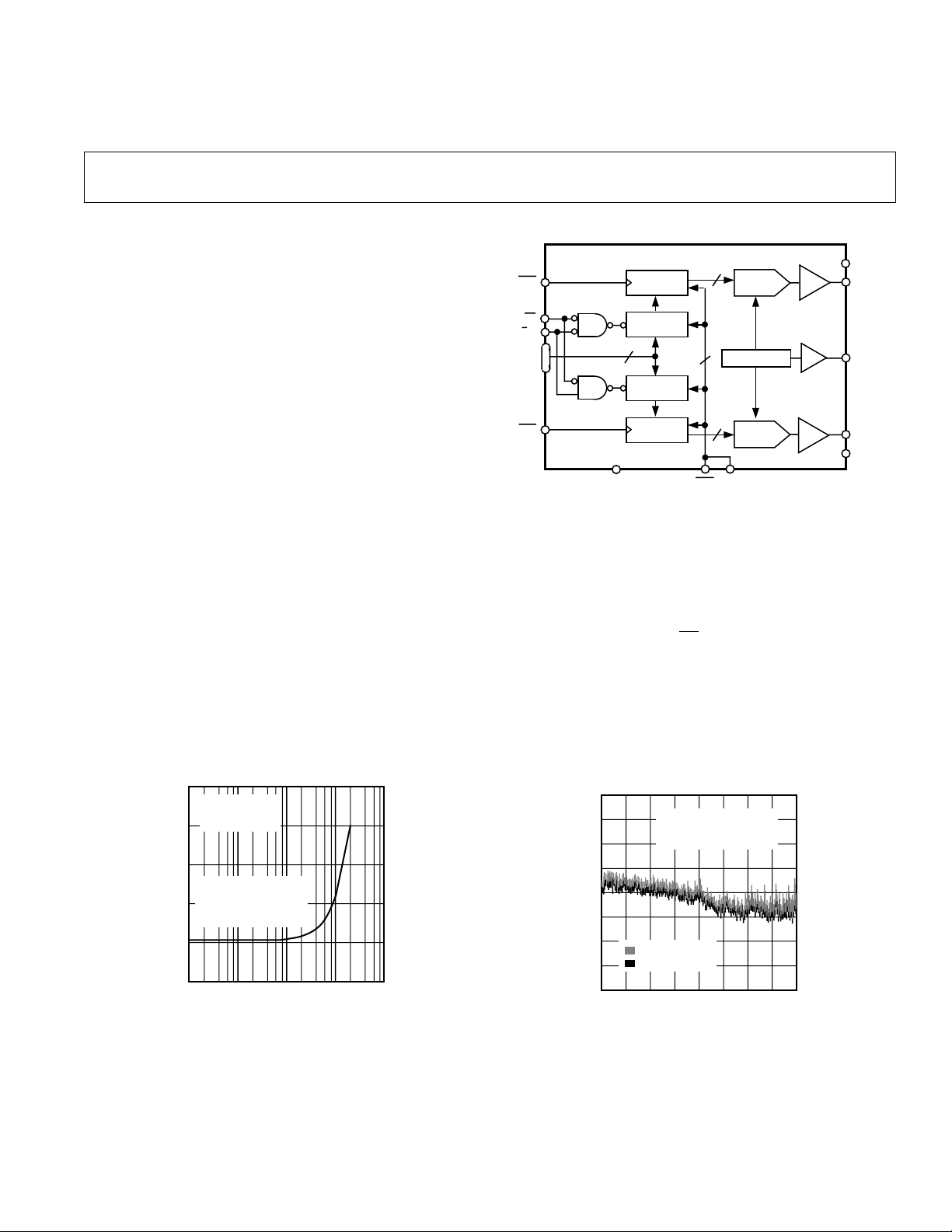
FUNCTIONAL BLOCK DIAGRAM
The high speed parallel data interface connects to the fastest
processors without wait states. The double-buffered input structure allows the user to load the input registers one at a time,
then a single load strobe tied to both LDA + LDB inputs will
update both DAC outputs simultaneously. LDA and LDB can
also be activated independently to immediately update their respective DAC registers. An address input decodes DAC A or
DAC B when the chip select
nous reset input sets the output to zero scale. The MSB bit can
be used to establish a preset to midscale when the reset input is
strobed.
The AD8582 is available in the 24-pin plastic DIP and the surface mount SOIC-24. Each part is fully specified for operation
over –40°C to +85°C, and the full +5 V ± 5% power supply
range.
CS input is strobed. An asynchro-
REV. 0
Information furnished by Analog Devices is believed to be accurate and
reliable. However, no responsibility is assumed by Analog Devices for its
use, nor for any infringements of patents or other rights of third parties
which may result from its use. No license is granted by implication or
otherwise under any patent or patent rights of Analog Devices.
4.6
PROPER OPERATION
MIN – Volts
DD
V
4.4
4.2
4.0
0.01
WHEN V
VOLTAGE ABOVE
SUPPLY
DD
CURVE
0.1 100101.0
OUTPUT LOAD CURRENT – mA
Figure 1. Minimum Supply Voltage vs. Load
Figure 2. Linearity Error vs. Digital Code and Temperature
One Technology Way, P.O. Box 9106, Norwood. MA 02062-9106, U.S.A.
Tel: 617/329-4700 Fax: 617/326-8703

AD8582–SPECIFICA TIONS
ELECTRICAL CHARACTERISTICS
(@ VDD = +5.0 V ± 5%, RL = No Load, –40°C ≤ TA ≤ +85°C, unless otherwise noted)
Parameter Symbol Condition Min Typ Max Units
STATIC PERFORMANCE
Resolution N Note 1 12 Bits
Relative Accuracy INL –2 ±3/4 +2 LSB
Differential Nonlinearity DNL Monotonic –1 ±3/4 +1 LSB
Zero-Scale Error V
Full-Scale Voltage V
ZSE
FS
Full-Scale Tempco TCV
FS
Data = 000
H
Data = FFFH,
2
4.079 4.095 4.111 V
+0.2 +3 mV
Notes 2 and 3 ±16 ppm/°C
MATCHING PERFORMANCE
Linearity Matching Error ∆VFSA/B ±1 LSB
REFERENCE OUTPUT
Output Voltage V
Output Source Current I
REF
REF
Line Rejection LN
Load Regulation LD
REJ
REG
Note 4 –5 mA
I
= 0 mA to 5 mA 0.1 %/mA
REF
2.484 2.500 2.516 V
0.08 %/V
ANALOG OUTPUT
Output Current I
Load Regulation at Half Scale LD
Capacitive Load C
DYNAMIC CHARACTERISTICS
Crosstalk C
Voltage Output Settling Time
3
5
Digital Feedthrough F
t
OUT
REG
L
T
S
T
Data = 800
RL = 402 Ω to ∞, Data = 800
No Oscillation
H
3
H
1 3 LSB
500 pF
±5mA
>64 dB
To ±1 LSB of Final Value 16 µs
Signal Measured at DAC Output, While 35 nV s
Changing Data (LDA = LDB = “1”)
LOGIC INPUTS
Logic Input Low Voltage V
Logic Input High Voltage V
Input Leakage Current I
Input Capacitance C
TIMING SPECIFICATIONS
3, 6
Chip Select Pulse Width t
DAC Select Setup t
DAC Select Hold t
Data Setup t
Data Hold t
Load Setup t
Load Hold t
Load Pulse Width t
Reset Pulse Width t
IL
IH
IL
IL
CSW
AS
AH
DS
DH
LS
LH
LDW
RSW
2.4 V
Note 3 10 pF
30 ns
30 ns
0ns
30 ns
10 ns
20 ns
10 ns
20 ns
30 ns
0.8 V
10 µA
SUPPLY CHARACTERISTICS
Positive Supply Current I
Power Dissipation
7
DD
P
DISS
VIH = 2.4 V, VIL = 0.8 V 4 7 mA
V
= 0 V, VDD = +5 V 1 2 mA
IL
VIH = 2.4 V, VIL = 0.8 V 20 35 mW
V
= 0 V, V
IL
= +5 V 5 10 mW
DD
Power Supply Sensitivity PSS ∆VDD = ±5% 0.002 0.004 %/%
NOTES
1
1 LSB = 1 mV for 0 V to +4.095 V output range.
2
Includes internal voltage reference error.
3
These parameters are guaranteed by design and not subject to production testing.
4
Very little sink current is available at the V
5
Settling time is not guaranteed for the first six codes 0 through 5.
6
All input control signals are specified with tR = tF = 5 ns (10% to 90% of +5 V) and timed from a voltage level of 1.6 V.
7
Power dissipation is a calculated value IDD × 5 V.
Specifications subject to change without notice.
pin. Use external buffer if setting up a virtual ground.
REF
–2–
REV. 0
AD8582
WARNING!
ESD SENSITIVE DEVICE
V
OUTA
AGND
V
OUTB
V
REF
MSB
DB0 DB11
DGND V
DD
DB1 DB10
DB2 DB9
DB3 DB8
DB4 DB7
DB5 DB6
14
1
2
24
23
5
6
7
20
19
18
3
4
22
21
8
17
9
16
10
15
11
TOP VIEW
(Not to Scale)
12
13
AD8582
LDA
RST
LDB
CS
A/B
TOP VIEW
(Not to Scale)
12
13
AD8582
1
24
ABSOLUTE MAXIMUM RATINGS*
VDD to DGND & AGND . . . . . . . . . . . . . . . . . . . –0.3 V, +7 V
Logic Inputs to DGND . . . . . . . . . . . . . . .–0.3 V, V
V
to AGND . . . . . . . . . . . . . . . . . . . . .–0.3 V, VDD + 0.3 V
OUT
V
to AGND . . . . . . . . . . . . . . . . . . . . .–0.3 V, VDD + 0.3 V
REF
AGND to DGND . . . . . . . . . . . . . . . . . . . . . . . . . –0.3 V, V
I
Short Circuit to GND . . . . . . . . . . . . . . . . . . . . . . 50 mA
OUT
Package Power Dissipation . . . . . . . . . . . . . . .(T
Thermal Resistance, θ
JA
+ 0.3 V
DD
max–TA)/θ
J
DD
JA
24-Pin Plastic DIP Package (N-24) . . . . . . . . . . . . . 62°C/W
24-Lead SOIC Package (SOL-24) . . . . . . . . . . . . . . 73°C/W
Maximum Junction Temperature (T
max) . . . . . . . . . . 150°C
J
Operating Temperature Range . . . . . . . . . . . . .–40°C to +85°C
Storage Temperature Range . . . . . . . . . . . . .–65°C to +150°C
Lead Temperature (Soldering, 10 sec) . . . . . . . . . . . . . +300°C
*Stresses above those listed under “Absolute Maximum Ratings” may cause
permanent damage to the device. This is a stress rating only and functional
operation of the device at these or any other conditions above those indicated in the
operational sections of this specification is not implied. Exposure to absolute
maximum rating conditions for extended periods may affect device reliability.
t
CSW
t
t
AS
t
DS
t
LS
AH
t
DH
t
t
S
LDW
± 1LSB
ERROR BAND
t
LH
t
RSW
t
S
A/B
D0–D11
LDA, LDB
RST
V
OUT
CS
Timing Diagram
PIN DESCRIPTION
Pin No. Name Description
1, 24 V
V
OUTA
OUTB
Voltage outputs from the DACs. Fixed
output voltage range of 0 V to 4.095 V
with 1 mV/LSB. An internal
temperature stabilized reference
maintains a fixed full-scale voltage
independent of time, temperature and
power supply variations.
2 AGND Analog Ground. Ground reference for
the internal bandgap reference voltage,
the DAC, and the output buffer.
3 DGND Digital ground for input logic.
4, 21
LDA, Load DAC register strobes. Transfers
LDB input register data to the DAC registers.
Active low inputs, Level sensitive latch.
May be connected together to double-
buffer load DAC registers.
5 MSB Digital Input: High presets DAC
registers to half scale (800
clears DAC registers to zero (000
upon
RST assertion.
6
RST Active low digital input that clears the
), Low
H
)
H
DAC register to zero, setting the DAC
to minimum scale when MSB pin = 0,
or half-scale when MSB pin = 1.
7–18 DB
Twelve Binary Data Bit Inputs. DB11 is
0–11
the MSB and DB0 is the LSB.
19
20
22 V
23 V
CS Chip Select. Active low input.
A/B Select DAC A = 0 or DAC B = 1.
DD
REF
Positive Supply. Nominal value +5 V, ± 5%.
Nominal 2.5 V reference output
voltage. This node must be buffered if
required to drive external loads.
Model Range Description Option
AD8582AN –40°C to +85°C 24-Pin Plastic DIP N-24
AD8582AR –40°C to +85°C 24-Lead SOIC SOL-24
AD8582Chips +25°C Die
*For die specifications contact your local Analog Devices sales office. The
AD8582 contains 1270 transistors.
CAUTION
ESD (electrostatic discharge) sensitive device. Electrostatic charges as high as 4000 V readily
accumulate on the human body and test equipment and can discharge without detection.
Although the AD8582 features proprietary ESD protection circuitry, permanent damage may
occur on devices subjected to high energy electrostatic discharges. Therefore, proper ESD
precautions are recommended to avoid performance degradation or loss of functionality.
REV. 0
ORDERING INFORMATION*
Temperature Package Package
–3–
PIN CONFIGURATIONS
N-24
24-Pin Plastic DIP
SOL-24
24-Pin SOIC

AD8582
R1
R2
V
OUT
RAIL-TO-RAIL
OUTPUT
AMPLIFIER
R
BANDGAP
REFERENCE
V
REF
2.5V
2R
R
2R
2R
SPDT
N CH FET
SWITCHES
2R
AV = 4.095/2.5
= 1.638V/V
VOLTAGE SWITCHED 12-BIT
R-2R D/A CONVERTER
BUFFER
2R
Table I. Control Logic Truth Table
CS A/B LDA LDB RST MSB Input Register DAC Register
LL HHHX Write to A Latched
LHHHHX Write to B Latched
LLLHH X Write to A A Transparent
L H H L H X Write to B B Transparent
H X L L H X Latched A & B Transparent
H X ^ ^ H X Latched Latched
XXXXLL Reset to Zero Scale Reset to Zero Scale
XXXXLH Reset to Midscale Reset to Midscale
HXXX^ X Latch Reset Value Latch Reset Value
^Denotes positive edge triggered.
OPERATION
The AD8582 is a complete, ready-to-use dual 12-bit digital-toanalog converter. Only one +5 V power supply is necessary for
operation. It contains two voltage-switched, 12-bit, lasertrimmed digital-to-analog converters, a curvature-corrected
bandgap reference, rail-to-rail output op amps, input registers,
and DAC registers. The parallel data interface consists of twelve
data bits, DB0–DB11, an address select pin
strobe pins (
tion an asynchronous
zero causing the V
LDA, LDB) and an active low CS strobe. In addi-
RST pin will set all DAC register bits to
to become zero volts, or to midscale for
OUT
trimming applications when the MSB pin is programmed to
Logic 1. This function is useful for power on reset or system
failure recovery to a known state.
A/B, two load
D/A CONVERTER SECTION
The internal DAC is a 12-bit voltage-mode device with an
output that swings from AGND potential to the 2.5 volt internal bandgap voltage. It uses a laser trimmed R-2R
ladder which is switched by N channel MOSFETs. The output voltage of the DAC has a constant resistance independent
of digital input code. The DAC output (not available to the
user) is internally connected to the rail-to-rail output op amp.
AMPLIFIER SECTION
The internal DAC’s output is buffered by a low power consumption precision amplifier. This low power amplifier contains
a differential PNP pair input stage which provides low offset
voltage and low noise, as well as the ability to amplify the zeroscale DAC output voltages. The rail-to-rail amplifier is configured in a gain of 1.6384 (= 4.095 V/2.5 V) in order to set the
4.095 volt full-scale output (1 mV/LSB). See Figure 3 for an
equivalent circuit schematic of the analog section.
The op amp has a 16 µs typical settling time to 0.01%. There
are slight differences in settling time for negative slewing signals
versus positive. See the oscilloscope photos in the Typical Performances section of this data sheet.
Figure 3. Equivalent Schematic of Analog Portion
OUTPUT SECTION
The rail-to-rail output stage of this amplifier has been designed
to provide precision performance while operating near either
power supply. Figure 4 shows an equivalent output schematic of
the rail-to-rail amplifier with its N channel pull-down FETs that
will pull an output load directly to GND. The output sourcing
current is provided by a P channel pull-up device that can supply GND terminated loads, especially important at the –5%
supply tolerance value of 4.75 volts.
V
DD
P-CH
V
N-CH
OUT
AGND
Figure 4. Equivalent Analog Output Circuit
–4–
REV. 0

AD8582
Figures 5 and 6 in the typical performance characteristics section provide information on output swing performance near
ground and full-scale as a function of load. In addition to resistive load driving capability, the amplifier has also been carefully
designed and characterized for up to 500 pF capacitive load
driving capability.
REFERENCE SECTION
The internal 2.5 V curvature-corrected bandgap voltage reference is laser trimmed for both initial accuracy and low temperature coefficient. The voltage generated by the reference is
available at the V
pin. Since V
REF
is not intended to drive ex-
REF
ternal loads, it must be buffered. The equivalent emitter follower output circuit of the V
Bypassing the V
pin will improve noise performance; how-
REF
pin is shown in Figure 3.
REF
ever, bypassing is not required for proper operation. Figure 8
shows broadband noise performance.
POWER SUPPLY
The very low power consumption of the AD8582 is a direct result of a circuit design optimizing use of the CBCMOS process.
By using the low power characteristics of the CMOS for the
logic, and the low noise, tight matching of the complementary
bipolar transistors good analog accuracy is achieved.
For power-consumption sensitive applications it is important to
note that the internal power consumption of the AD8582 is
strongly dependent on the actual logic-input voltage levels
present on the DB0–DB11,
CS, A/B, MSB, LDA, LDB and
RST pins. Since these inputs are standard CMOS logic struc-
tures they contribute static power dissipation dependent on the
actual driving logic V
and VOL voltage levels. The graph in
OH
Figure 9 shows the effect on total AD8582 supply current as a
function of the actual value of input logic voltage. Consequently, for optimum dissipation use of CMOS logic versus
TTL provides minimal dissipation in the static state. A V
INL
=
0 V on the DB0–11 pins provides the lowest standby dissipation
of 1 mA typical with a +5 V power supply.
As with any analog system, it is recommended that the AD8582
power supply be bypassed on the same PC card that contains
the chip. Figure 10 shows the power supply rejection versus frequency performance. This should be taken into account when
using higher frequency switched-mode power supplies with
ripple frequencies of 100 kHz and higher.
One advantage of the rail-to-rail output amplifiers used in the
AD8582 is the wide range of usable supply voltage. The part is
fully specified and tested over temperature for operation from
+4.75 V to +5.25 V. If reduced linearity and source current
capability near full scale can be tolerated, operation of the
AD8582 is possible down to +4.3 volts. The minimum operating supply voltage versus load current plot, in Figure 1, provides information for operation below V
TIMING AND CONTROL
= +4.75 V.
DD
The input registers are level triggered and acquire data from the
data bus during the time period when
ister selected is determined by the
for a complete description. When
latched into the register and held until
CS is low. The input reg-
A/B select pin, see Table I.
CS goes high, the data is
CS returns low. The
minimum time required for the data to be present on the bus
before
CS returns high is called the data setup time (tDS) as seen
in Timing Diagram. The data hold time (t
of time that the data has to remain on the bus after
) is the amount
DH
CS goes
high. The high speed timing offered by the AD8582 provides
for direct interface with no wait states in all but the fastest
microprocessors.
The data from the input registers is transferred to the DAC registers by the active low
LDA and LDB pins. If these inputs are
tied together, a single logic input can perform a double buffer
update of the DAC registers, which in turn simultaneously
changes the analog output voltages to a new value. If the
and
LDB pins are wired low, they become transparent. In this
LDA
mode the input register data will directly control the output
voltages. Refer to the Control Logic Truth
Table for a com-
plete description.
Unipolar Output Operation
This is the basic mode of operation for the AD8582. The
AD8582 has been designed to drive loads as low as 820Ω in parallel with 500 pF. The code table for this operation is shown in
Table II.
Table II. Unipolar Code Table
Hexadecimal
Number in DAC Decimal Number Analog Output
Register in DAC Register Voltage (V)
FFF 4095 + 4.095
801 2049 + 2.049
800 2048 + 2.048
7FF 2047 + 2.047
000 0 0
REV. 0
–5–

AD8582–Typical Performance Characteristics
0
5
VDD = +5V
T
A
= +25°C
OUTPUT VOLTAGE
1mV/DIV
DATA
TIME – 5µs/DIV
15µs
5
4
3
2
OUTPUT VOLTAGE – Volts
1
0
10
100 100k10k1k
LOAD RESISTANCE – Ω
VDD = +5V
T
= +25°C
A
RL TIED TO AGND
DATA = FFF
RL TIED TO +5V
DATA = 000
H
H
Figure 5. Output Swing vs. Load
TA = +25°C
NBW = 630kHz
100
VDD = +5V
DATA = 000
10
1
TA = +85°C
0.1
OUTPUT PULL-DOWN VOLTAGE – mV
0.01
1
H
TA = –40°C
TA = +25°C
10 1000100
OUTPUT SINK CURRENT – µA
Figure 6. Pull-Down Voltage vs.
Output Sink Current Capability
5
4
3
2
VDD = +4.75V
TA = +25°C
VDD = +5V
80
60
40
20
0
–20
–40
OUTPUT CURRENT – mA
–60
–80
POSITIVE0
CURRENT0
LIMIT0
1
OUTPUT VOLTAGE – Volts
Figure 7. I
100
VDD = +5V ±200mV AC
80
60
40
T
DATA = FFF
OUT
= +25°C
A
DATA = 800
RL TIED TO +2V
NEGATIVE
CURRENT
LIMIT
vs. V
OUT
H
H
32
OUTPUT NOISE VOLTAGE – 200µV/DIV
TIME = 100µs/DIV
Figure 8. Broadband Noise
5
LD
0
2.048
2.038
– Volts
2.028
OUT
V
2.018
2.008
204810 TO 2047
TIME – 500ns/DIV
10
Figure 11. Midscale Transition
Performance
SUPPLY CURRENT – mA
1
0
0
LOGIC VOLTAGE VALUE – Volts
3241
5
Figure 9. Supply Current vs. Logic
Input Voltage
5
INPUT
0
4
3
2
OUTPUT
1
0
5V
100
LDB
90
V
= +5V
DD
= +25°C
T
A
10
0%
1V
TIME = 20µs/DIV
20µs
Figure 12. Large Signal Settling Time
20
POWER SUPPLY REJECTION – dB
0
10
100 100k10k1k
FREQUENCY – Hz
Figure 10. Power Supply Rejection
vs. Frequency
Figure 13. Output Voltage Rise
Time Detail
–6–
REV. 0

AD8582
4.115
4.075
125
4.085
4.080
–25–50
4.095
4.090
4.100
4.105
4.110
1007550250
TEMPERATURE – °C
FULL-SCALE OUTPUT – Volts
VDD = +4.75V
NO LOAD
SS = 298 UNITS
AVG
σAVG +1σ
σAVG –1σ
HOURS OF OPERATION AT +150°C
3
–3
600
0
–2
100
–1
0
2
1
500400300200
NOMINAL FULL-SCALE
VOLTAGE CHANGE – mV
VDD = +5V
SS = 135 UNITS
DATA = FFF
H
AVG
σAVG +2
σ
σAVG –2
σ
1
0
DATA
V
OUT
10mV/DIV
TIME – 5µs/DIV
10
90
100
0%
10mV
5V 5µs
CS = HIGH
VDD = +5V
T
= +25°C
5
DATA
0
15µs
1mV/DIV
OUTPUT VOLTAGE
A
TIME – 5µs/DIV
Figure 14. Output Voltage Fall
Time Detail
3
VDD = +4.75V
NO LOAD
2
SS = 298 UNITS
1
45
40
35
30
25
20
FREQUENCY
15
10
5
0
–8 1–5 0–7 –6
TOTAL UNADJUSTED ERROR – mV
TUE = ΣINL+ZS+FS
SS = 297 UNITS
V
DD
T
A
–4 –3 –2 –1
= +4.75V
= +25°C
Figure 15. Total Unadjusted Error
Histogram
100
Hz
10
VDD = +5V
TA = +25°C
DATA = FFF
H
Figure 16. Full-Scale Voltage vs.
Temperature
0
ZERO-SCALE OUTPUT – Volts
–1
Figure 17. Zero-Scale Voltage vs.
Temperature
8
7
6
5
4
3
2
SUPPLY CURRENT – mA
1
0
Figure 20. Supply Current vs.
Temperature
REV. 0
–25–50
TEMPERATURE – °C
VDD = +5.25V
VDD = +4.75V
–25–50
V
DATA
NO LOAD
VDD = +5.00V
TEMPERATURE – °C
1007550250
= +2.4V
1007550250
125
125
1.0
OUTPUT NOISE DENSITY – µV/
0.1
10
100 100k10k1k
FREQUENCY – Hz
Figure 18. Output Voltage Noise
Density vs. Frequency
2V
100
90
V
DD
0V
V
REF
10
0V
0%
2V
∞TA = +25°C
R
VDD = +5V
TIME – 1µs/DIV
Figure 21. Reference Startup vs.
Time
–7–
L
Figure 19. Long-Term Drift
Accelerated by Burn-In
1µs
= ∞
Figure 22. Digital Feedthrough vs.
Time

AD8582
0.10
0.00
125–25
0.02
–50
0.06
0.04
0.08
10050 75
0
25
TEMPERATURE – °C
REF LINE REGULATION – %/Volt
σAVG +1σ
AVG
σAVG – 1σ
∆ VDD = +4.75 TO +5.25V
10
8
VDD = +4.75V
6
4
2
σAVG +1σ
0
AVG
–2
–4
REFERENCE ERROR – mV
–6
σAVG –1σ
–8
–10
–25
–50
25
0
10050 75
TEMPERATURE – °C
Figure 23. Reference Error vs.
Temperature
125
0.000
–0.001
σAVG +1σ
–0.002
∆VDD = +4.75V
∆I
AVG
= 5mA
L
–0.003
–0.004
REF LOAD REGULATION – %/mA
–0.005
–50
σAVG –1σ
125–25
25
0
10050 75
TEMPERATURE – °C
Figure 24. Reference Load Regulation
vs. Temperature
OUTLINE DIMENSIONS
Dimensions shown in inches and (mm).
N-24
24-Pin Narrow Body Plastic DIP
C1869–18–12/93
Figure 25. Reference Line Regulation
vs. Temperature
PIN 1
0.210
(5.33)
MAX
0.200 (5.05)
0.125 (3.18)
PIN 1
0.0118 (0.30)
0.0040 (0.10)
24
1
0.022 (0.558)
0.014 (0.356)
24
1
1.275 (32.30)
1.125 (28.60)
0.100 (2.54)
BSC
0.070 (1.77)
0.045 (1.15)
SOL-24
24-Lead Wide Body SOIC
13
0.2992 (7.60)
0.2914 (7.40)
12
0.6141 (15.60)
0.5985 (15.20)
0.0500 (1.27)
BSC
0.0192 (0.49)
0.0138 (0.35)
0.1043 (2.65)
0.0926 (2.35)
0.0125 (0.32)
0.0091 (0.23)
13
0.280 (7.11)
0.240 (6.10)
12
0.060 (1.52)
0.015 (0.38)
SEATING
PLANE
0.4193 (10.65)
0.3937 (10.00)
0.150
(3.81)
MIN
8
0
°
°
0.325 (8.25)
0.300 (7.62)
0.0291 (0.74)
0.0098 (0.25)
0.0500 (1.27)
0.0157 (0.40)
0.195 (4.95)
0.115 (2.93)
0.015 (0.381)
0.008 (0.204)
x 45
°
PRINTED IN U.S.A.
–8–
REV. 0
 Loading...