

ANALOG DEVICES AD8392A Service Manual
Low Power, High Output Current, Quad Op
V
V
www.BDTIC.com/ADI
Amp, Dual-Channel ADSL/ADSL2+ Line Driver
FEATURES
Four current feedback, high current amplifiers
Ideal for use as ADSL/ADSL2+ dual-channel central office
(
CO) line drivers
Low power operation
Power supply operation from ±5 V (+10 V) up to ±12 V (+24 V)
Less than 3 mA/amp quiescent supply current for full
po
wer ADSL/ADSL2+ CO applications (20.4 dBm line
power, 5.5 CF)
Three active power modes plus shutdown
High output voltage and current drive
500 mA peak output drive current
42.6 V p-p differential output voltage
Low distortion
−93 dBc @1 MHz second harmonic
−103 dBc @ 1 MHz third harmonic
High speed: 515 V/μs differential slew rate
Additional functionality of AD8392AACP
On-chip, common-mode voltage generation
APPLICATIONS
ADSL/ADSL2+ CO line drivers
XDSL line drives
GENERAL DESCRIPTION
The AD8392A is comprised of four high output current, low
power consumption, operational amplifiers. It is particularly
well suited for the CO driver interface in digital subscriber line
systems, such as ADSL and ADSL2+. The driver is capable of
providing enough power to deliver 20.4 dBm to a line, while
compensating for losses due to hybrid insertion and back
termination resistors.
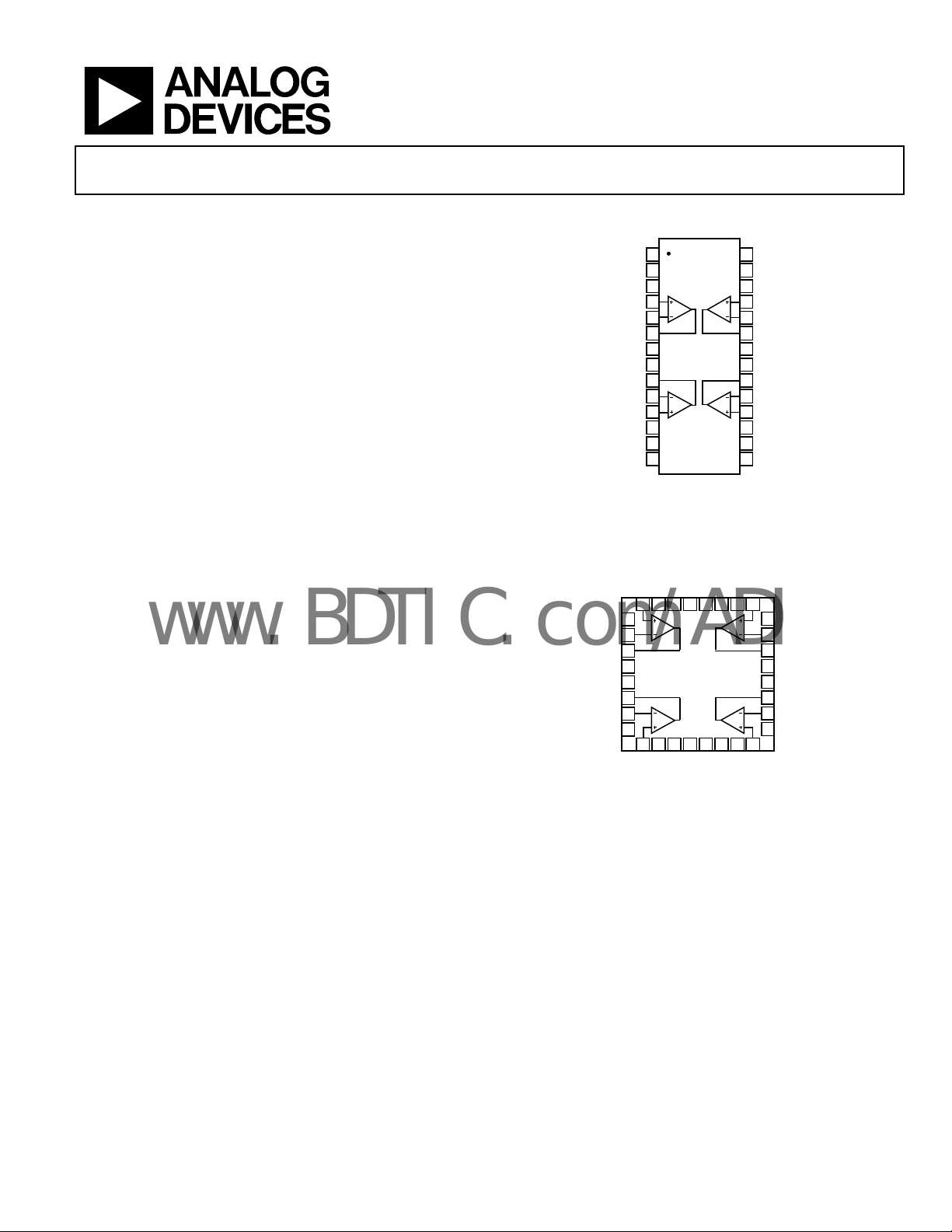
AD8392A
PIN CONFIGURATIONS
V
1
EE
2
PD0 1, 2
3
PD1 1, 2
1
+V
4
V
V
–V
OUT
OUT
–V
+V
GND
IN
IN
V
NC
IN
IN
NC
NC
1
1
5
1
6
7
CC
AD8392A
8
3
9
3
10
34
3
11
12
13
14
NC = NO CONNECT
Figure 1. AD8392AARE, 28-Lead TSSOP/EP
1
IN
+V
32 31 30 29 28 27 2526
1
NC
2
1
–V
IN
3
1
OUT
4
V
CC
5
NC
6
3
OUT
7
–V
3
IN
8
NC
91011121314
3
+V
NC = NO CONNECT
Figure 2. AD8392AACP, 5 mm × 5 mm, 32-Lead LFCSP
PD1 1, 2
1
3
IN
NC
V
PD0 1, 2
AD8392A
3, 4
GND
COM
V
28
GND
27
NC
26
NC
2
+V
25
2
EE
GND
EE
V
IN
–V
2
24
IN
V
2
23
OUT
22
NC
21
V
CC
20
V
4
OUT
19
–VIN4
18
4
+V
IN
17
PD1 3, 4
16
PD0 3, 4
15
V
EE
06477-001
1, 2
2
IN
COM
V
NC
+V
24
2
4
PD0 3, 4
NC
–V
2
23
IN
2
V
22
OUT
21
NC
V
20
CC
V
4
19
OUT
–VIN4
18
17
NC
1615
4
IN
+V
PD1 3, 4
06477-002
The AD8392A is available in two thermally enhanced packages,
a 28-lead
TSSOP/EP (AD8392AARE) and a 5 mm × 5 mm,
32-lead LFCSP (AD8392AACP). Four bias modes are available
via the use of two digital bits (PD1, PD0).
Additionally, the AD8392AACP provides V
pins for on-chip,
COM
common-mode voltage generation.
The low power consumption, high output current, high output
volt
age swing, and robust thermal packaging enable the
AD8392A to be used as the CO line drivers in ADSL and other
xDSL systems.
Rev. 0
Information furnished by Analog Devices is believed to be accurate and reliable. However, no
responsibility is assumed by Anal og Devices for its use, nor for any infringements of patents or ot her
rights of third parties that may result from its use. Specifications subject to change without notice. No
license is granted by implication or otherwise under any patent or patent rights of Analog Devices.
Trademarks and registered trademarks are the property of their respective owners.
One Technology Way, P.O. Box 9106, Norwood, MA 02062-9106, U.S.A.
Tel: 781.329.4700 www.analog.com
Fax: 781.461.3113 ©2006 Analog Devices, Inc. All rights reserved.

AD8392A
www.BDTIC.com/ADI
TABLE OF CONTENTS
Features .............................................................................................. 1
Applications........................................................................................8
Applications....................................................................................... 1
General Description......................................................................... 1
Pin Configurations ...........................................................................1
Specifications..................................................................................... 3
Absolute Maximum Ratings............................................................ 4
Thermal Resistance ...................................................................... 4
ESD Caution.................................................................................. 4
Typical Performance Characteristics............................................. 5
Theory of Operation ........................................................................ 7
REVISION HISTORY
10/06—Revision 0: Initial Version
Supplies, Grounding, and Layout................................................8
Power Management ......................................................................8
Thermal Considerations...............................................................8
Typical ADSL/ADSL2+ Application...........................................9
Multitone Power Ratio............................................................... 10
Outline Dimensions ....................................................................... 11
Ordering Guide .......................................................................... 11
Rev. 0 | Page 2 of 12
AD8392A
www.BDTIC.com/ADI
SPECIFICATIONS
VS = ±12 V or +24 V, RL = 100 Ω, G = +5, PD = (0, 0), T = 25°C, unless otherwise noted.
Table 1.
Parameter Min Typ Max Unit Test Conditions/Comments
DYNAMIC PERFORMANCE
−3 dB Small Signal Bandwidth 25 37 MHz V
−3 dB Large Signal Bandwidth 23 30 MHz V
Peaking 0.06 dB V
Slew Rate 515 V/μs V
NOISE/DISTORTION PERFORMANCE
Second Harmonic Distortion −93 dBc fC = 1 MHz, V
Third Harmonic Distortion −103 dBc fC = 1 MHz, V
Multitone Input Power Ratio 70 dBc 26 kHz to 2.2 MHz, Z
Voltage Noise (RTI) 2.5 nV/√Hz f = 10 kHz
+Input Current Noise 7.6 pA/√Hz f = 10 kHz
−Input Current Noise 12.5 pA/√Hz f = 10 kHz
INPUT CHARACTERISTICS
RTI Offset Voltage −4 ±2 +4 mV V
+Input Bias Current 2 7 μA
−Input Bias Current 3 10 μA
Input Resistance 8 MΩ
Input Capacitance 1 pF
Common-Mode Rejection Ratio 63 66 dB (ΔV
OUTPUT CHARACTERISTICS
Differential Output Voltage Swing 41.2 42.6 V p-p ΔV
Single-Ended Output Voltage Swing 20.6 21.3 V p-p ΔV
Linear Output Current 500 mA RL = 10 Ω, fC = 100 kHz
POWER SUPPLY
Operating Range (Dual Supply) ±5 ±12 V
Operating Range (Single Supply) 10 24 V
Total Quiescent Current
PD1, PD0 = (0, 0) 5.8 6.5 mA/amp
PD1, PD0 = (0, 1) 3.0 3.5 mA/amp
PD1, PD0 = (1, 0) 2.6 3.0 mA/amp
PD1, PD0 = (1, 1) (Shutdown State) 0.4 0.08 mA/amp
PD = 0 Threshold 0.8 V
PD = 1 Threshold 1.8 V
+Power Supply Rejection Ratio 72 74 dB ΔV
−Power Supply Rejection Ratio 65 69 dB ΔV
= 0.1 V p-p, RF = 2 kΩ
OUT
= 4 V p-p, RF = 2 kΩ
OUT
= 0.1 V p-p, RF = 2 kΩ
OUT
= 20 V p-p, RF = 2 kΩ
OUT
= 2 V p-p
OUT
= 2 V p-p
OUT
− V
+IN
−IN
)/(ΔV
OS, DM (RTI)
OUT
, RL = 50 Ω
OUT
OS, DM (RTI)
OS, DM (RTI)
IN, CM
/ΔVCC, ΔVCC = ±1 V
/ΔVEE, ΔVEE = ±1 V
= 100 Ω differential load
LINE
)
Rev. 0 | Page 3 of 12
AD8392A
www.BDTIC.com/ADI
ABSOLUTE MAXIMUM RATINGS
Table 2.
Parameter Rating
Supply Voltage ±13 V (+26 V)
RMS output voltages should be considered. If R
to V
as in single-supply operation, the total power is VS × I
S−
In single supply with R
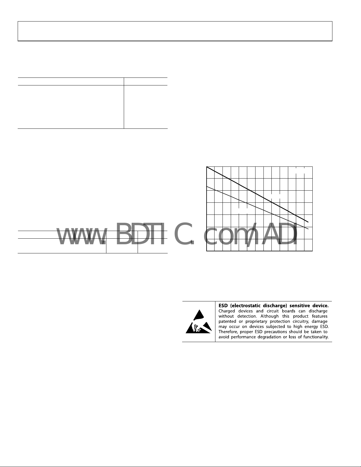
Power Dissipation See Figure 3
Storage Temperature Range −65°C to +150°C
Operating Temperature Range −40°C to +85°C
Lead Temperature (Soldering 10 sec) 300°C
Junction Temperature 150°C
Stresses above those listed under Absolute Maximum Ratings
may cause permanent damage to the device. This is a stress
rating only; functional operation of the device at these or any
other conditions above those indicated in the operational
section of this specification is not implied. Exposure to absolute
maximum rating conditions for extended periods may affect
device reliability.
Airflow increases heat dissipation, effectively reducing θ
addition, more metal directly in contact with the package leads
from metal traces, through holes, ground, and power planes
reduces the θ
.
JA
Figure 3 shows the maximum safe power dissipation in the
ackage vs. the ambient temperature for the LFCSP-32 and
p
TSSOP-28/EP packages on a JEDEC standard 4-layer board.
θ
values are approximations.
JA
7
6
to VS−, worst case is V
L
is referenced
L
= VS/2.
OUT
TJ = 150°C
JA
. In
OUT
.
THERMAL RESISTANCE
θJA is specified for the worst-case conditions, that is, θJA is specified
for the device soldered in the circuit board for surface-mount
packages.
Table 3.
Package Type θ
JA
LFCSP-32 (CP) 27.27 °C/W
TSSOP-28/EP (RE) 35.33 °C/W
Maximum Power Dissipation
The power dissipated in the package (PD) is the sum of the
quiescent power dissipation and the power dissipated in the
package due to the load drive for all outputs. The quiescent
power is the voltage between the supply pins (V
quiescent current (I
the total drive power is V
in the package and some in the load (V
). Assuming that the load (RL) is midsupply,
S
/2 × I
S
, some of which is dissipated
OUT
× I
OUT
OUT
Unit
) times the
S
).
5
4
3
2
1
MAXIMUM POWER DISSIP ATION (W )
0
–40 –30 –20 –10 0 10 20 30 40 50 60 70 80 90
Figure 3. Maximum Power Dissipation vs. Temperature for a 4-Layer Board
TSSOP-28/EP
TEMPERATURE (° C)
LFCSP-32
6477-003
See the Thermal Considerations section for additional thermal
design guidance.
ESD CAUTION
Rev. 0 | Page 4 of 12
 Loading...