0.8 GHz–2.5 GHz
a
FEATURES
High Accuracy
1 Degree rms Quadrature Error @ 1.9 GHz
0.2 dB I/Q Amplitude Balance @ 1.9 GHz
Broad Frequency Range: 0.8 GHz–2.5 GHz
Sideband Suppression: –46 dBc @ 0.8 GHz
Sideband Suppression: –36 dBc @ 1.9 GHz
Modulation Bandwidth: DC–70 MHz
0 dBm Output Compression Level @ 0.8 GHz
Noise Floor: –147 dBm/Hz
Single 2.7 V–5.5 V Supply
Quiescent Operating Current: 45 mA
Standby Current: 1 A
16-Lead TSSOP Package
APPLICATIONS
Digital and Spread Spectrum Communication Systems
Cellular/PCS/ISM Transceivers
Wireless LAN/Wireless Local Loop
QPSK/GMSK/QAM Modulators
Single-Sideband (SSB) Modulators
Frequency Synthesizers
Image Reject Mixer
Quadrature Modulator
AD8346
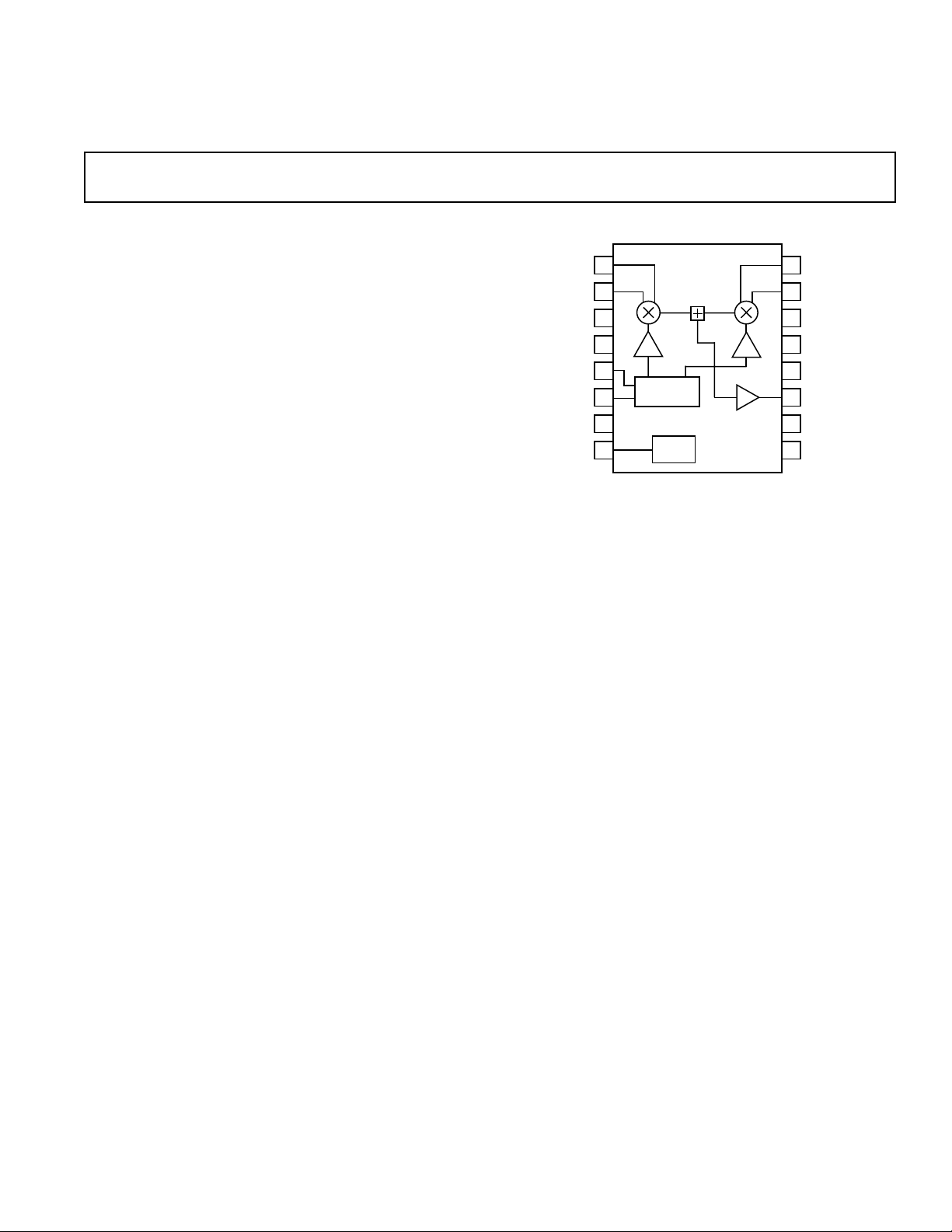
FUNCTIONAL BLOCK DIAGRAM
IBBP
1
IBBN
2
COM1
3
COM1
4
LOIN
5
LOIP
VPS1
ENBL
6
7
8
PHASE
SPLITTER
BIAS
AD8346
QBBP
16
QBBN
15
COM4
14
COM4
13
VPS2
12
VOUT
11
COM3
10
COM2
9
PRODUCT DESCRIPTION
The AD8346 is a silicon RFIC I/Q modulator for use from
0.8 GHz to 2.5 GHz. Its excellent phase accuracy and amplitude balance allow high performance direct modulation to RF.
The differential LO input is applied to a polyphase network
phase splitter that provides accurate phase quadrature from
0.8 GHz to 2.5 GHz. Buffer amplifiers are inserted between
two sections of the phase splitter to improve the signal-to-noise
ratio. The I and Q outputs of the phase splitter drive the LO
inputs of two Gilbert-cell mixers. Two differential V-to-I converters connected to the baseband inputs provide the baseband
modulation signals for the mixers. The outputs of the two mixers
are summed together at an amplifier which is designed to drive a
50 Ω load.
REV. 0
Information furnished by Analog Devices is believed to be accurate and
reliable. However, no responsibility is assumed by Analog Devices for its
use, nor for any infringements of patents or other rights of third parties
which may result from its use. No license is granted by implication or
otherwise under any patent or patent rights of Analog Devices.
This quadrature modulator can be used as the transmit modulator in digital systems such as PCS, DCS, GSM, CDMA, and
ISM transceivers. The baseband quadrature inputs are directly
modulated by the LO signal to produce various QPSK and
QAM formats at the RF output.
Additionally, this quadrature modulator can be used with direct
digital synthesizers in hybrid phase-locked loops to generate
signals over a wide frequency range with millihertz resolution.
The AD8346 is supplied in a 16-lead TSSOP package, measur-
ing 6.5 × 5.1 × 1.1 mm. It is specified to operate over a
–40°C to +85°C temperature range and 2.7 V to 5.5 V supply
voltage range. The device is fabricated on Analog Devices’ high
performance 25 GHz bipolar silicon process.
One Technology Way, P.O. Box 9106, Norwood, MA 02062-9106, U.S.A.
Tel: 781/329-4700 World Wide Web Site: http://www.analog.com
Fax: 781/326-8703 © Analog Devices, Inc., 1999

AD8346–SPECIFICATIONS
(VS = 5 V; TA = +25ⴗC, LO frequency = 1900 MHz; LO level = –10 dBm; BB frequency
= 100 kHz; BB inputs are dc biased to 1.2 V; BB input level = 1.0 V p-p each pin for 2.0 V p-p differential drive; LO source and RF output load
impedances are 50 ⍀, dBm units are referenced to 50 ⍀ unless otherwise noted.)
Parameters Conditions Min Typ Max Units
RF OUTPUT
Operating Frequency 0.8 2.5 GHz
Quadrature Phase Error (See Figure 29 for Setup) 1 Degree rms
I/Q Amplitude Balance (See Figure 29 for Setup) 0.2 dB
Output Power I and Q Channels in Quadrature –13 –10 –6 dBm
Output VSWR 1.25:1
Output P1 dB –3 dBm
Carrier Feedthrough –42 –35 dBm
Sideband Suppression –36 –25 dBc
IM3 Suppression –60 dBc
Equivalent Output IP3 +20 dBm
Output Noise Floor 20 MHz Offset from LO –147 dBm/Hz
RESPONSE TO CDMA IS95
BASEBAND SIGNALS
ACPR (Adjacent Channel Power Ratio) (See Figure 29 for Setup) –72 dBc
EVM (Error Vector Magnitude) (See Figure 29 for Setup) 2.5 %
Rho (Waveform Quality Factor) (See Figure 29 for Setup) 0.9974
MODULATION INPUT
Input Resistance 12 kΩ
Modulation Bandwidth –3 dB 70 MHz
LO INPUT
LO Drive Level –12 –6 dBm
Input VSWR 1.9:1
ENABLE
ENBL HI Threshold 2.0 V
ENBL LO Threshold 0.5 V
ENBL Turn-On Time Settle to Within 0.5 dB of Final
SSB Output Power 2.5 µs
ENBL Turn-Off Time Time for Supply Current to Drop
Below 2 mA 12 µs
POWER SUPPLIES
Voltage 2.7 5.5 V
Current Active (ENBL HI) 35 45 55 mA
Current Standby (ENBL LO) 1 20 µA
Specifications subject to change without notice.
–2–
REV. 0

AD8346
WARNING!
ESD SENSITIVE DEVICE
ABSOLUTE MAXIMUM RATINGS*
Supply Voltage VPS1, VPS2 . . . . . . . . . . . . . . . . . . . . . . 5.5 V
Input Power LOIP, LOIN (re. 50 Ω) . . . . . . . . . . . . +10 dBm
Min Input Voltage IBBP, IBBN, QBBP, QBBN . . . . . . . . 0 V
*Stresses above those listed under Absolute Maximum Ratings may cause perma-
nent damage to the device. This is a stress rating only; functional operation of the
device at these or any other conditions above those indicated in the operational
section of this specification is not implied. Exposure to absolute maximum rating
conditions for extended periods may effect device reliability.
Max Input Voltage IBBP, IBBN, QBBP, QBBN . . . . . . . 2.5 V
Internal Power Dissipation . . . . . . . . . . . . . . . . . . . . 500 mW
. . . . . . . . . . . . . . . . . . . . . . . . . . . . . . . . . . . . . . 125°C/W
θ
JA
Operating Temperature Range . . . . . . . . . . . –40°C to +85°C
Storage Temperature Range . . . . . . . . . . . . –65°C to +150°C
Lead Temperature Range (Soldering 60 sec) . . . . . . . .+300°C
CAUTION
ESD (electrostatic discharge) sensitive device. Electrostatic charges as high as 4000 V readily
accumulate on the human body and test equipment and can discharge without detection.
Although the AD8346 features proprietary ESD protection circuitry, permanent damage may
occur on devices subjected to high energy electrostatic discharges. Therefore, proper ESD
precautions are recommended to avoid performance degradation or loss of functionality.
ORDERING GUIDE
Package
Model Temperature Range Package Description Option
AD8346ARU –40°C to +85°C Tube (16-Lead TSSOP) Thin Shrink Small Outline Package RU-16
AD8346ARU-REEL 13" Tape and Reel
AD8346ARU-REEL7 7" Tape and Reel
AD8346-EVAL Evaluation Board
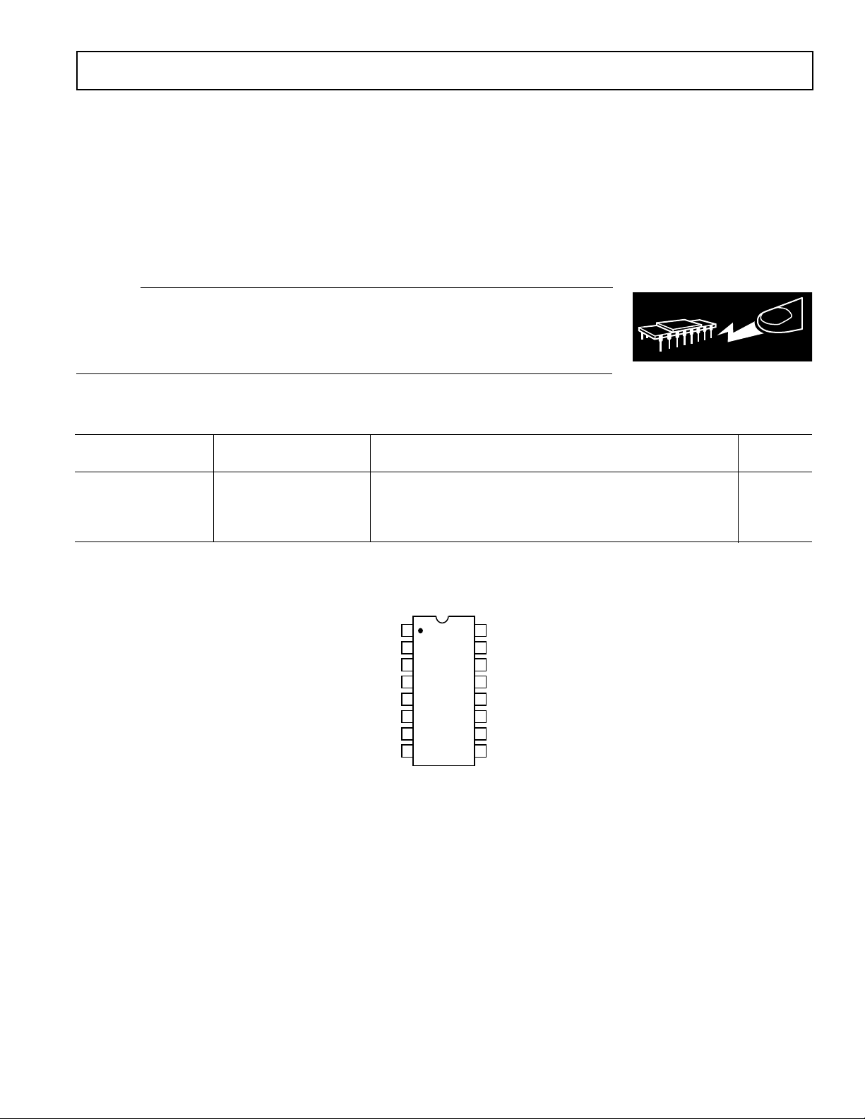
PIN CONFIGURATION
1
IBBP QBBP
IBBN QBBN
2
3
COM1 COM4
4
COM1 COM4
LOIN VPS2
LOIP VOUT
VPS1 COM3
ENBL COM2
AD8346
TOP VIEW
5
(Not to Scale)
6
7
8
16
15
14
13
12
11
10
9
REV. 0
–3–

AD8346
43V
43V
VPS2
V
OUT
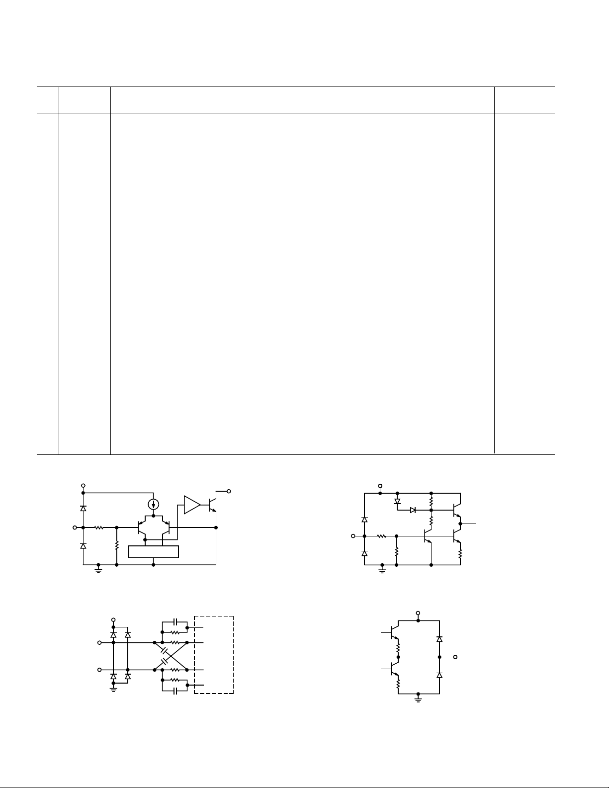
PIN FUNCTION DESCRIPTIONS
Equivalent
Pin Name Description Circuit
1 IBBP I Channel Baseband Positive Input Pin. Input should be dc biased to approximately 1.2 V. Circuit A
Nominal characterized ac swing is 1 V p-p (0.7 V to 1.7 V). This makes the differential
input 2 V p-p when IBBN is 180 degrees out of phase from IBBP.
2 IBBN I Channel Baseband Negative Input Pin. Input should be dc biased to approximately 1.2 V. Circuit A
Nominal characterized ac swing is 1 V p-p (0.7 V to 1.7 V). This makes the differential
input 2 V p-p when IBBN is 180 degrees out of phase from IBBP.
3 COM1 Ground pin for the LO phase splitter and LO buffers.
4 COM1 Ground pin for the LO phase splitter and LO buffers.
5 LOIN LO Negative Input Pin. Internal dc bias (approximately VPS1–800 mV) is supplied. This Circuit B
pin must be ac coupled.
6 LOIP LO Positive Input Pin. Internal dc bias (approximately VPS1–800 mV) is supplied. This Circuit B
pin must be ac coupled.
7 VPS1 Power supply pin for the bias cell and LO buffers. This pin should be decoupled using
local 100 pF and 0.01 µF capacitors.
8 ENBL Enable Pin. A high level enables the device; a low level puts the device in sleep mode. Circuit C
9 COM2 Ground pin for the input stage of output amplifier.
10 COM3 Ground pin for the output stage of output amplifier.
11 VOUT 50 Ω DC Coupled RF Output. User must provide ac coupling on this pin. Circuit D
12 VPS2 Power supply pin for Baseband input voltage to current converters and mixer core. This pin
should be decoupled using local 100 pF and 0.01 µF capacitors.
13 COM4 Ground pin for Baseband input voltage to current converters and mixer core.
14 COM4 Ground pin for Baseband input voltage to current converters and mixer core.
15 QBBN Q Channel Baseband Negative Input. Input should be dc biased to approximately 1.2 V. Circuit A
Nominal characterized ac swing is 1 V p-p. This makes the differential input 2 V p-p when
QBBN is 180 degrees out of phase from QBBP.
16 QBBP Q Channel Baseband Positive Input. Input should be dc biased to approximately 1.2 V. Circuit A
Nominal characterized ac swing is 1 V p-p. This makes the differential input 2 V p-p when
QBBN is 180 degrees out of phase from QBBP.
INPUT
VPS2
LOIN
LOIP
9kV
3kV
VPS1
ACTIVE LOADS
Circuit A
Circuit B
BUFFER
CONTINUES
PHASE
SPLITTER
TO MIXER
CORE
ENBL
Figure 1. Equivalent Circuits
–4–
VPS1
30kV
40kV
Circuit C
Circuit D
75kV
75kV
TO BIAS FOR
STARTUP/
SHUTDOWN
780V
REV. 0
 Loading...