Analog Devices AD8345ARE-REEL7, AD8345ARE-REEL, AD8345ARE, AD8345 Datasheet
250 MHz–1000 MHz
a
FEATURES
250 MHz–1000 MHz Operating Frequency
+2.5 dBm P1 dB @ 800 MHz
–155 dBm/Hz Noise Floor
0.5 Degree RMS Phase Error (IS95)
0.2 dB Amplitude Balance
Single 2.7 V–5.5 V Supply
Pin-Compatible with AD8346
16-Lead Exposed Paddle TSSOP Package
APPLICATIONS
Cellular Communication Systems
W-CDMA/CDMA/GSM/PCS/ISM Transceivers
Fixed Broadband Access Systems LMDS/MMDS
Wireless LAN
Wireless Local Loop
Digital TV/CATV Modulators
Single Sideband Upconverter
Quadrature Modulator
AD8345
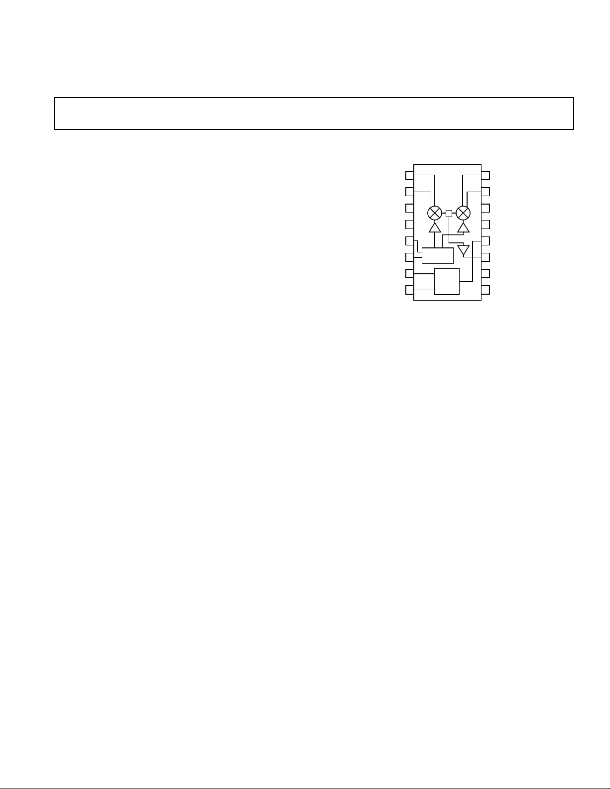
FUNCTIONAL BLOCK DIAGRAM
IBBP
IBBN
COM3
COM1
LOIN
LOIP
VPS1
ENBL
1
2
3
4
5
6
7
8
AD8345
PHASE
SPLITTER
BIAS
+
16
15
14
13
12
11
10
9
QBBP
QBBN
COM3
COM3
VPS2
VOUT
COM2
COM3
PRODUCT DESCRIPTION
The AD8345 is a silicon RFIC quadrature modulator, designed
for use from 250 MHz to 1000 MHz. Its excellent phase accuracy and amplitude balance enable the high performance direct
modulation of an IF carrier.
The AD8345 accurately splits the external LO signal into two
quadrature components through the polyphase phase-splitter
network. The two I and Q LO components are mixed with the
baseband I and Q differential input signals. Finally, the outputs
of the two mixers are combined in the output stage to provide a
single-ended 50 Ω drive at VOUT.
APPLICATIONS
The AD8345 Modulator can be used as the IF transmit modulator in digital communication systems such as GSM and PCS
transceivers. It can also directly modulate an LO signal to
produce QPSK and various QAM formats for 900 MHz communication systems as well as digital TV and CATV systems.
Additionally, this quadrature modulator can be used with direct
digital synthesizers in hybrid phase-locked loops to generate
signals over a wide frequency range with millihertz resolution.
The AD8345 Modulator is supplied in a 16-lead TSSOP package with exposed paddle. Its performance is specified over a
–40°C to +85°C temperature range. This device is fabricated on
Analog Devices’ advanced silicon bipolar process.
REV. 0
Information furnished by Analog Devices is believed to be accurate and
reliable. However, no responsibility is assumed by Analog Devices for its
use, nor for any infringements of patents or other rights of third parties that
may result from its use. No license is granted by implication or otherwise
under any patent or patent rights of Analog Devices.
One Technology Way, P.O. Box 9106, Norwood, MA 02062-9106, U.S.A.
Tel: 781/329-4700 www.analog.com
Fax: 781/326-8703 © Analog Devices, Inc., 2001

AD8345–SPECIFICATIONS
(VS = 5 V; LO= –2 dBm @ 800 MHz, 50 ⍀ source and load impedances, I and Q inputs
0.7 V ⴞ 0.3 V on each side for a 1.2 V p-p differential input, I and Q inputs driven in quadrature @ 1 MHz Baseband Frequency.
TA = 25ⴗC, unless otherwise noted.)
Parameters Conditions Min Typ Max Unit
RF OUTPUT
Operating Frequency
1
250 1000 MHz
Output Power –3 –1 +2 dBm
Output P1 dB 2.5 dBm
Noise Floor 20 MHz Offset from LO, All BB –155 dBm/Hz
Inputs at 0.7 V
Quadrature Error (CDMA IS95 Setup, Refer to Figure 13) 0.5 Degree rms
I/Q Amplitude Balance (CDMA IS95 Setup, Refer to Figure 13) 0.2 dB
LO Leakage –42 –33 dBm
Sideband Rejection –42 –34 dBc
Third Order Distortion –52 dBc
Second
Order Distortion –60 dBc
Equivalent Output IP3 25 dBm
Equivalent Output IP2 59 dBm
Output Return Loss (S22) –20 dB
RESPONSE TO CDMA IS95 (Refer to Figure 13)
BASEBAND SIGNALS
ACPR –72 dBc
EVM 1.3 %
Rho 0.9995
LO INPUT
LO Drive level –10 –2 0 dBm
LOIP Input Return Loss (S11)
2
No Termination on LOIP, LOIN at –5 dB
AC Ground
50 Ω Terminating Resistor, Differential –9 dB
Drive via Balun
BASEBAND INPUTS
Input Bias Current 10 µA
Input Capacitance 2pF
DC Common Level 0.6 0.7 0.8 V
Bandwidth (3 dB) Full Power (0.7 V ± 0.3 V on Each 80 MHz
Input, Refer to TPC 2)
ENABLE
Turn-On Enable High to Output within 0.5 dB of 2.5 µs
Final Value
Turn-Off Enable Low to Supply Current Dropping 1.5 µs
below 2 mA
ENBL High Threshold (Logic 1) +V
/2 V
S
ENBL Low Threshold (Logic 0) +VS/2 V
POWER SUPPLIES
Voltage 2.7 5.5 V
Current Active 50 65 78 mA
Current Standby 70 µA
NOTES
1
For information on operation below 250 MHz, see Figure 4.
2
See LO Drive section for more details on input matching.
Specifications subject to change without notice.
–2–
REV. 0
AD8345
16
15
14
13
12
11
10
9
QBBP
QBBN
COM3
COM3
VPS2
VOUT
COM2
COM3
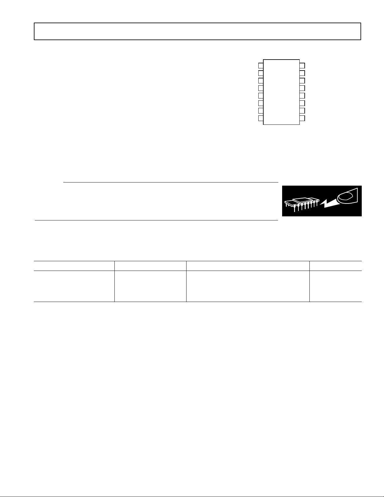
1
2
3
4
5
6
7
8
IBBP
IBBN
COM3
COM1
LOIN
LOIP
VPS1
ENBL
AD8345
TOP VIEW
(Not to Scale)
ABSOLUTE MAXIMUM RATINGS*
PIN CONFIGURATION
Supply Voltage VPS1, VPS2 . . . . . . . . . . . . . . . . . . . . . 5.5 V
Input Power LOIP, LOIN (re 50 Ω) . . . . . . . . . . . . . 10 dBm
IBBP, IBBN, QBBP, QBBN . . . . . . . . . . . . . . . . . 0 V, 2.5 V
Internal Power Dissipation . . . . . . . . . . . . . . . . . . . . 500 mW
(Exposed Paddle Soldered Down) . . . . . . . . . . . . 30°C/W
θ
JA
(Exposed Paddle not Soldered Down) . . . . . . . . . 95°C/W
θ
JA
Maximum Junction Temperature . . . . . . . . . . . . . . . . 150°C
Operating Temperature Range . . . . . . . . . . . –40°C to +85°C
Storage Temperature Range . . . . . . . . . . . . –65°C to +150°C
Lead Temperature Range (Soldering 60 sec) . . . . . . . . 300°C
*Stresses above those listed under Absolute Maximum Ratings may cause perma-
nent damage to the device. This is a stress rating only; functional operation of the
device at these or any other conditions above those indicated in the operational
section of this specification is not implied. Exposure to absolute maximum rating
conditions for extended periods may affect device reliability.
CAUTION
ESD (electrostatic discharge) sensitive device. Electrostatic charges as high as 4000 V readily
accumulate on the human body and test equipment and can discharge without detection. Although
the AD8345 features proprietary ESD protection circuitry, permanent damage may occur on
devices subjected to high-energy electrostatic discharges. Therefore, proper ESD precautions are
recommended to avoid performance degradation or loss of functionality.
WARNING!
ESD SENSITIVE DEVICE
ORDERING GUIDE
Model Temperature Range Package Description Package Option
AD8345ARE –40°C to +85°C Tube (16-Lead TSSOP with Exposed Pad) RE-16
AD8345ARE-REEL 13" Tape and Reel
AD8345ARE-REEL7 7" Tape and Reel
AD8345-EVAL Evaluation Board
REV. 0
–3–
AD8345
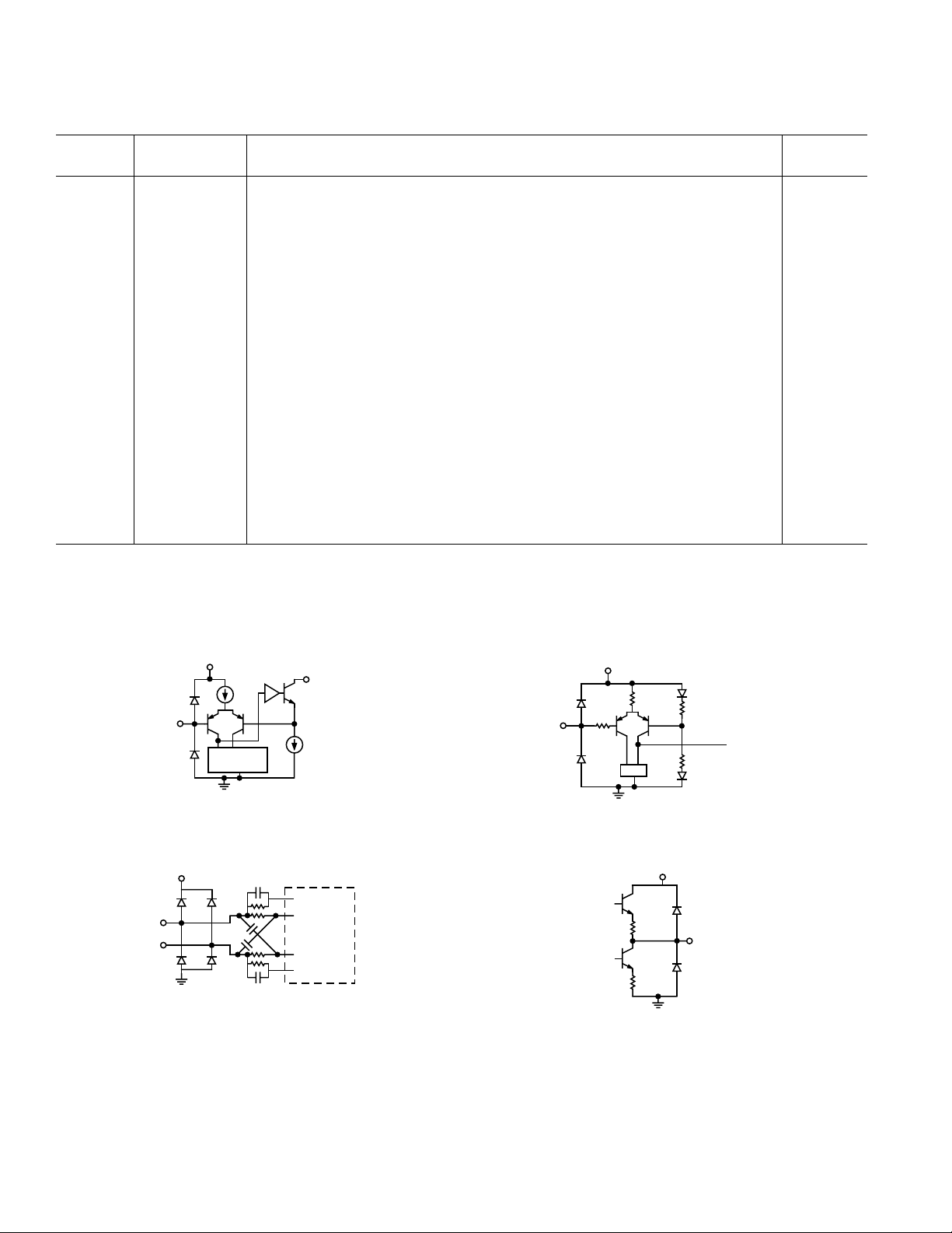
PIN FUNCTION DESCRIPTIONS
Equivalent
Pin No. Mnemonic Function Circuit
1, 2 IBBP, IBBN I Channel Baseband Differential Input Pins. These high impedance inputs should Circuit A
be dc biased to approximately 0.7 V. Nominal characterized ac swing is 0.6 V p-p
on each pin (0.4 V to 1 V). This gives a differential drive of 1.2 V p-p. Inputs are
not self-biasing so external biasing circuitry must be used in ac-coupled applications.
3, 9, 13, 14 COM3 Ground Pin for Input V-to-I Converters and Mixer Core.
4 COM1 Ground Pin for the LO Phase-Splitter and LO Buffers.
5, 6 LOIN, LOIP Differential LO Drive Pins. Internal dc bias (approximately 1.8 V @ V
is supplied. Pins must be ac-coupled. Single-ended or differential drive is permissible.
7 VPS1 Power Supply Pin for the Bias Cell and LO Buffers. This pin should be decoupled
using local 1000 pF and 0.01 µF capacitors.
8 ENBL Enable Pin. A high level enables the device; a low level puts the device in sleep mode. Circuit C
10 COM2 Ground Pin for the Output Stage of Output Amplifier.
11 VOUT 50 Ω DC-Coupled RF Output. Pin should be ac-coupled. Circuit D
12 VPS2 Power supply pin for baseband input voltage to current converters and mixer core.
This pin should be decoupled using local 1000 pF and 0.01 µF capacitors.
15, 16 QBBN, QBBP Q Channel Baseband Differential Input Pins. Inputs should be dc biased to Circuit A
approximately 0.7 V. Nominal characterized ac swing is 0.6 V p-p on each pin
(0.4 V to 1 V). This gives a differential drive level of 1.2 V p-p. Inputs are not
self-biasing so external biasing circuitry must be used in ac-coupled applications.
= 5 V) Circuit B
S
EQUIVALENT CIRCUITS
VPS2
INPUT
CURRENT
MIRROR
Circuit A
VPS1
LOIN
LOIP
Circuit B
BUFFER
TO MIXER
CORE
PHASE
SPLITTER
CONTINUES
Figure 1. Equivalent Circuits
ENBL
VPS2
100k⍀
Circuit C
VPS2
40⍀
40⍀
Circuit D
100k⍀
100k⍀
VOUT
TO BIAS FOR
STARTUP/
SHUTDOWN
–4–
REV. 0
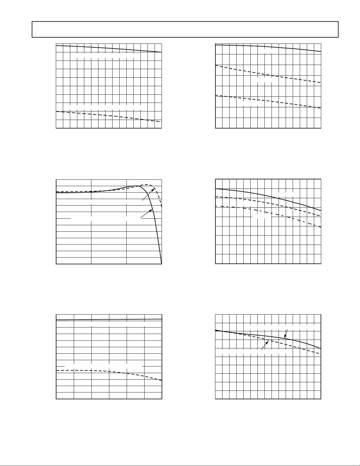
Typical Performance Characteristics–
AD8345
0
–2
–4
–6
–8
–10
–12
SSB POWER – dBm
–14
–16
–18
–20
250
V
= 5V, DIFFERENTIAL INPUT = 1.2V p-p
S
VS = 2.7V, DIFFERENTIAL INPUT = 200mV p-p
300 350 400 450 500 550 600 650 700 750 800 850 900 950 1000
LO FREQUENCY – MHz
TPC 1. Single Sideband (SSB) Output Power (P
Frequency (F
Baseband Frequency (F
1.0
0.5
0.0
–0.5
–1.0
–1.5
–2.0
–2.5
–3.0
–3.5
–4.0
OUTPUT POWER VARIATION – dB
–4.5
–5.0
–5.5
). (I and Q Inputs Driven in Quadrature at
LO
VS = 2.7V, 5V DIFFERENTIAL INPUT = 200mV p-p
V
= 5V, DIFFERENTIAL INPUT = 1.2V p-p
S
0.1
) = 1 MHz; TA = 25°C)
BB
1 10 100
BASEBAND FREQUENCY – MHz
OUT
) vs. LO
0
TA = –40ⴗC
TA = +25ⴗC
500 800
LO FREQUENCY – MHz
–10
–12
SSB OUTPUT P1dB – dBm
–14
–16
–2
–4
–6
–8
TA = +85ⴗC
350 650 950300 400 450 550 600 700 750 850 900 1000
250
TPC 4. SSB Output 1 dB Compression Point (OP 1 dB) vs.
F
. (VS = 2.7 V, LO Level = –2 dBm, I and Q Inputs Driven
LO
in Quadrature, F
4.0
3.5
3.0
2.5
2.0
1.5
1.0
SSB OUTPUT P1dB – dBm
0.5
0.0
–0.5
250
= 1 MHz)
BB
TA = +85ⴗC
TA = +25ⴗC
TA = –40ⴗC
350 650 950300 400 450 550 600 700 750 850 900 1000
500 800
LO FREQUENCY – MHz
TPC 2. I and Q Input Bandwidth. (TA = 25°C, FLO = 800 MHz,
LO Level = –2 dBm, I and Q Inputs Driven in Quadrature)
0
–2
–4
–6
–8
–10
–12
–14
–16
SSB POWER – dBm
–18
–20
–22
–24
–26
TPC 3. SSB P
V
= 2.7V, DIFFERENTIAL INPUT = 200mV p-p
S
–40
–20 20 60
OUT
Level = –2 dBm, F
VS = 5V, DIFFERENTIAL INPUT = 1.2V p-p
04080
TEMPERATURE – ⴗC
vs. Temperature. (FLO = 800 MHz, LO
= 1 MHz, I and Q Inputs Driven in
BB
Quadrature)
REV. 0
TPC 5. SSB Output 1 dB Compression Point (OP 1 dB) vs.
F
. (VS = 5 V, LO Level = –2 dBm, I and Q Inputs Driven in
LO
Quadrature, F
–40
–41
–42
–43
–44
–45
–46
–47
–48
CARRIER FEEDTHROUGH – dBm
–49
–50
= 1 MHz)
BB
VS = 5V, DIFFERENTIAL INPUT = 1.2V p-p
VS = 2.7V, DIFFERENTIAL INPUT = 200mV p-p
350 650 950300 400 450 550 600 700 750 850 900 1000
250
500 800
LO FREQUENCY – MHz
TPC 6. Carrier Feedthrough vs. FLO. (LO Level = –2 dBm,
= 25°C)
T
A
–5–
 Loading...