Analog Devices AD8343 a Datasheet

DC-to-2.5 GHz
a
FEATURES
High-Performance Active Mixer
Broadband Operation to 2.5 GHz
Conversion Gain: 7.1 dB
Input IP3: 16.5 dBm
LO Drive: –10 dBm
Noise Figure: 14.1 dB
Input P1 dB: 2.8 dBm
Differential LO, IF and RF Ports
50 LO Input Impedance
Single-Supply Operation: 5 V @ 50 mA Typical
Power-Down Mode @ 20 A Typical
APPLICATIONS
Cellular Base Stations
Wireless LAN
Satellite Converters
SONET/SDH Radio
Radio Links
RF Instrumentation
High IP3 Active Mixer
AD8343
FUNCTIONAL BLOCK DIAGRAM
1
2
3
4
5
6
7
AD8343
BIAS
14
13
12
11
10
9
8
COMM
OUTP
OUTM
COMM
LOIP
LOIM
COMM
COMM
INPP
INPM
DCPL
VPOS
PWDN
COMM
PRODUCT DESCRIPTION
The AD8343 is a high-performance broadband active mixer.
Having wide bandwidth on all ports and very low intermodulation
distortion, the AD8343 is well suited for demanding transmit or
receive channel applications.
The AD8343 provides a typical conversion gain of 7.1 dB.
The integrated LO driver supports a 50 Ω differential input impedance with low LO drive level, helping to minimize external
component count.
The open-emitter differential inputs may be interfaced directly
to a differential filter or driven through a balun (transformer) to
provide a balanced drive from a single-ended source.
The open-collector differential outputs may be used to drive a
differential IF signal interface or convert to a single-ended signal
through the use of a matching network or transformer. When centered on the VPOS supply voltage, the outputs may swing ±1V.
The LO driver circuitry typically consumes 15 mA of current.
Two external resistors are used to set the mixer core current for
required performance resulting in a total current of 20 mA to
60 mA. This corresponds to power consumption of 100 mW to
300 mW with a single 5 V supply.
The AD8343 is fabricated on Analog Devices’ proprietary,
high-performance 25 GHz silicon bipolar IC process. The
AD8343 is available in a 14-lead TSSOP package. It operates
over a –40°C to +85°C temperature range. A device-populated
evaluation board is available to facilitate device matching.
REV. A
Information furnished by Analog Devices is believed to be accurate and
reliable. However, no responsibility is assumed by Analog Devices for its
use, nor for any infringements of patents or other rights of third parties that
may result from its use. No license is granted by implication or otherwise
under any patent or patent rights of Analog Devices.
One Technology Way, P.O. Box 9106, Norwood, MA 02062-9106, U.S.A.
Tel: 781/329-4700www.analog.com
Fax: 781/326-8703 © Analog Devices, Inc., 2002

AD8343–SPECIFICATIONS
BASIC OPERATING CONDITIONS
(VS = 5.0 V, TA = 25C)
Parameter Conditions Figure Min Typ Max Unit
INPUT INTERFACE (INPP, INPM)
Differential Open Emitter
DC Bias Voltage Internally Generated 1.1 1.2 1.3 V
Operating Current Each Input (I
Value of Bias Setting Resistor
) Current Set by R3, R4 24 5 16 20 mA
O
1
1% Bias Resistors; R3, R4 24 68.1 Ω
Port Differential Impedance f = 50 MHz; R3 and R4 = 68.1 Ω 9 2.7 + j 6.8 Ω
OUTPUT INTERFACE (OUTP, OUTM)
Differential Open Collector
DC Bias Voltage Externally Applied 4.5 5 5.5 V
Voltage Swing 1.65 V
Operating Current Each Output Same as Input Current I
± 1V
S
O
+ 2 V
S
mA
Port Differential Impedance f = 50 MHz 12 900 – j77 Ω
LO INTERFACE (LOIP, LOIM)
Differential Common Base Stage
DC Bias Voltage
2
Internally Generated; Port 300 360 450 mV
Typically AC-Coupled
LO Input Power 50 Ω Impedance 17 –12 –10 –3 dBm
Port Differential Return Loss 16 –10 dB
POWER-DOWN INTERFACE (PWDN)
PWDN Threshold Assured ON VS – 1.5 V
PWDN Response Time
3
Assured OFF V
Time from Device ON to OFF 4 2.2 µs
– 0.5 V
S
Time from Device OFF to ON 5 500 ns
PWDN Input Bias Current PWDN = 0 V (Device ON) –85 –195 µA
PWDN = 5 V (Device OFF) 0 µA
POWER SUPPLY
Supply Voltage Range 4.5 5.0 5.5 V
Total Quiescent Current R3 and R4 = 68.1 Ω 24 50 60 mA
Over Temperature 75 mA
Powered-Down Current V
= 5.5 V 20 95 µA
S
= 4.5 V 6 15 µA
V
S
Over Temperature, VS = 5.5 V 50 150 µA
NOTES
1
The balance in the bias current in the two legs of the mixer input may be important in applications where a low feedthrough of the Local Oscillator (LO) is critical.
2
This voltage is proportional to absolute temperature (PTAT). Reference section on DC-Coupling the LO for more information regarding this interface.
3
Response time until device meets all specified conditions.
Specifications subject to change without notice.
–2–
REV. A

AD8343
TOP VIEW
(Not to Scale)
14
13
12
11
10
9
8
1
2
3
4
5
6
7
COMM
AD8343
INPP
INPM
DCPL
VPOS
PWDN
COMM
COMM
OUTP
OUTM
COMM
LOIP
LOIM
COMM
Table I. Typical AC Performance
= 5.0 V, TA = 25C; See Figure 24 and Tables III Through V.)
(V
S
Input 1 dB
Input Frequency Output Frequency Conversion Gain SSB Noise Figure Input IP3 Compression Point
(MHz) (MHz) (dB) (dB) (dBm) (dBm)
RECEIVER CHARACTERISTICS
400 70 5.6 10.5 20.5 3.3
900 170 3.6 11.4 19.4 3.6
1900 170 7.1 14.1 16.5 2.8
2400 170 6.8 15.3 14.5 2.1
2400 425 5.4 16.2 16.5 2.2
TRANSMITTER CHARACTERISTICS
150 900 7.5 17.9 18.1 1.9
150 1900 0.25 16.0 13.4 0.8
Table II. Typical Isolation Performance
= 5.0 V, TA = 25C; See Figure 24 and Tables III Through V.)
(V
S
Input Frequency Output Frequency LO to Output 2 LO to Output 3 LO to Output Input to Output
(MHz) (MHz) Leakage (dBm) Leakage (dBm) Leakage (dBm) Leakage (dBm)
RECEIVER CHARACTERISTICS
400 70 –40.1 –51.0 –44.0 –62.4
900 170 –44.4 –35.5 < –75.0 –56.9
1900 170 –65.6 –38.3 –73.3 –65.7
2400 170 –66.7 –44.4 < –75.0 –73.7
2400 425 –51.1 –49.4 < –75.0 –52.3
TRANSMITTER CHARACTERISTICS
150 900 –27.6 < –75 dBm < –75 dBm –35.3
150 1900 < –75 dBm < –75 dBm < –75 dBm –69.7
Low-side LO injection used for typical performance.
ABSOLUTE MAXIMUM RATINGS
1
VPOS Quiescent Voltage . . . . . . . . . . . . . . . . . . . . . . . . 5.5 V
OUTP, OUTM Quiescent Voltage . . . . . . . . . . . . . . . . 5.5 V
INPP, INPM Voltage Differential . . . . . . . . . . . . . . . 500 mV
LOIP, LOIM Current (Injection or Extraction) . . . . . . 1 mA
LOIP, LOIM Voltage Differential . . . . . . . . . . . . . . . 500 mV
Internal Power Dissipation (TSSOP)
θ
(TSSOP) . . . . . . . . . . . . . . . . . . . . . . . . . . . . . . 125°C/W
JA
2
. . . . . . . . . . . . 320 mW
Maximum Junction Temperature . . . . . . . . . . . . . . . . . 125°C
Operating Temperature Range . . . . . . . . . . . –40°C to +85°C
Storage Temperature Range . . . . . . . . . . . . –65°C to +150°C
Lead Temperature Range (Soldering 60 sec) . . . . . . . . . 300°C
NOTES
1
Stresses above those listed under Absolute Maximum Ratings may cause perma-
nent damage to the device. This is a stress rating only; functional operation of the
device at these or any other conditions above those indicated in the operational
section of this specification is not implied. Exposure to absolute maximum rating
conditions for extended periods may affect device reliability.
2
A portion of the device power is dissipated by the external bias resistors R3 and R4.
Model Range Description Option
AD8343ARU RU-14
AD8343ARU-REEL –40°C to 14-Lead 13" Tape
AD8343ARU-REEL7 7" Tape
AD8343-EVAL Evaluation
ORDERING GUIDE
Temperature Package Package
+85°C Plastic and Reel
TSSOP
and Reel
Board
PIN CONFIGURATION
REV. A
–3–
AD8343
WARNING!
ESD SENSITIVE DEVICE
TO
MIXER
CORE
R1
10
DCPL
VPOS
LOIP
LOIM
2V
DC
360mV
DC
360mV
DC
BIAS
CELL
LO
BUFFER
PIN FUNCTION DESCRIPTIONS
TSSOP Name Function Simplified Interface Schematic
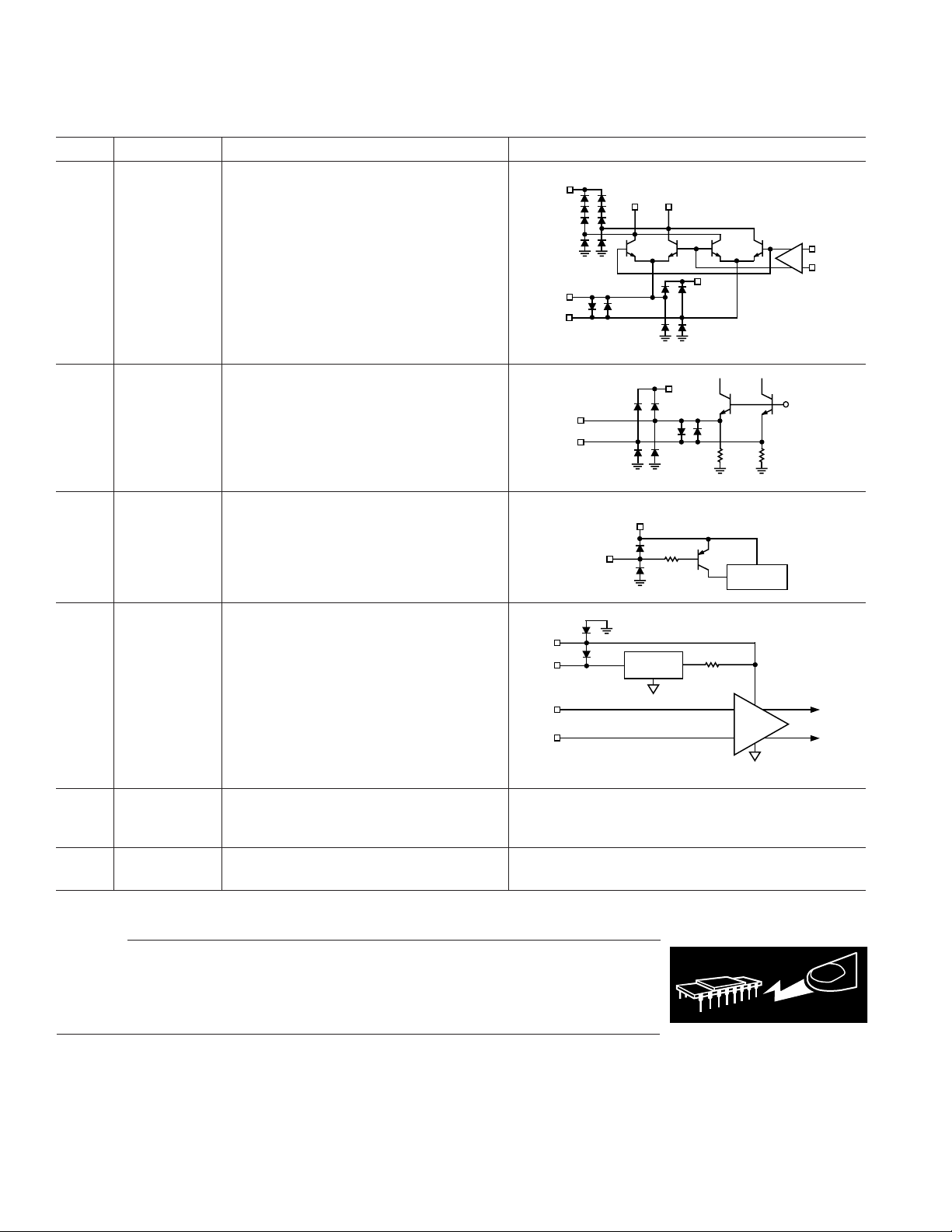
2, 3 INPP/INPM Differential input pins. Need to be dc-biased;
typically ac-coupled.
12, 13 OUTP/OUTM Open collector differential output pins.
Need to be dc-biased and ac-coupled.
VPOS
5V
INPP
INPM
DC
1.2V
1.2V
OUTP
OUTM
5V
5V
DC
DC
DC
DC
VPOS
5V
DC
LOIP
LOIM
9, 10 LOIP/LOIM Differential local oscillator (LO) input pins.
Typically ac-coupled.
6 PWDN Power-down interface. Connect pin to
ground for normal operating mode. Connect
pin to supply for power-down mode.
4 DCPL Bias rail decoupling capacitor connection
for LO driver.
5 VPOS Positive supply voltage (VS), 4.5 V to 5.5 V.
Ensure adequate supply bypassing for proper
device operation as shown in Figure 24.
1, 7, 8, COMM Connect to low impedance circuit ground.
11, 14
LOIP
LOIM
360mV
360mV
PWDN
DC
DC
VPOS
5V
DC
25k
VPOS
5V
DC
400
BIAS
CELL
VBIAS
400
CAUTION
ESD (electrostatic discharge) sensitive device. Electrostatic charges as high as 4000 V readily
accumulate on the human body and test equipment and can discharge without detection. Although
the AD8343 features proprietary ESD protection circuitry, permanent damage may occur on
devices subjected to high-energy electrostatic discharges. Therefore, proper ESD precautions are
recommended to avoid performance degradation or loss of functionality.
–4–
REV. A
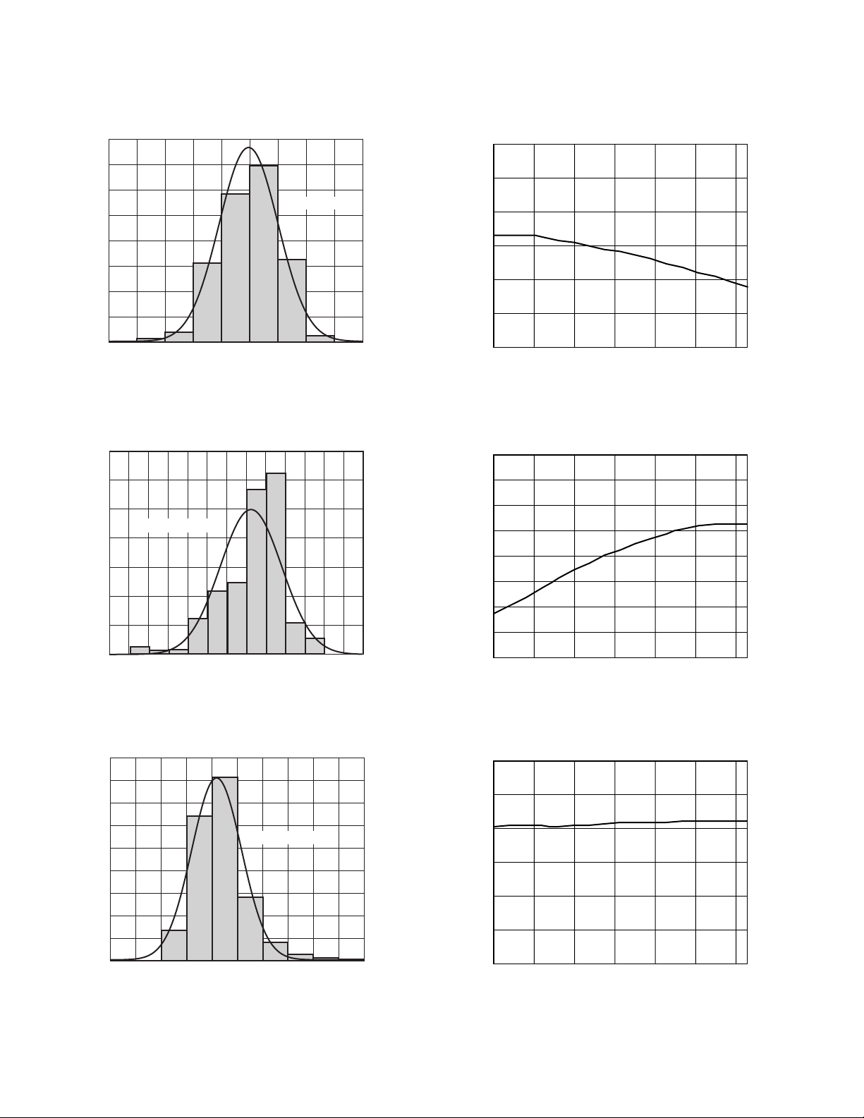
Typical Performance Characteristics–AD8343
RECEIVER CHARACTERISTICS (f
60
50
40
30
PERCENTAGE
20
10
0
5.42 5.47 5.52 5.57 5.62 5.67 5.72
5.37
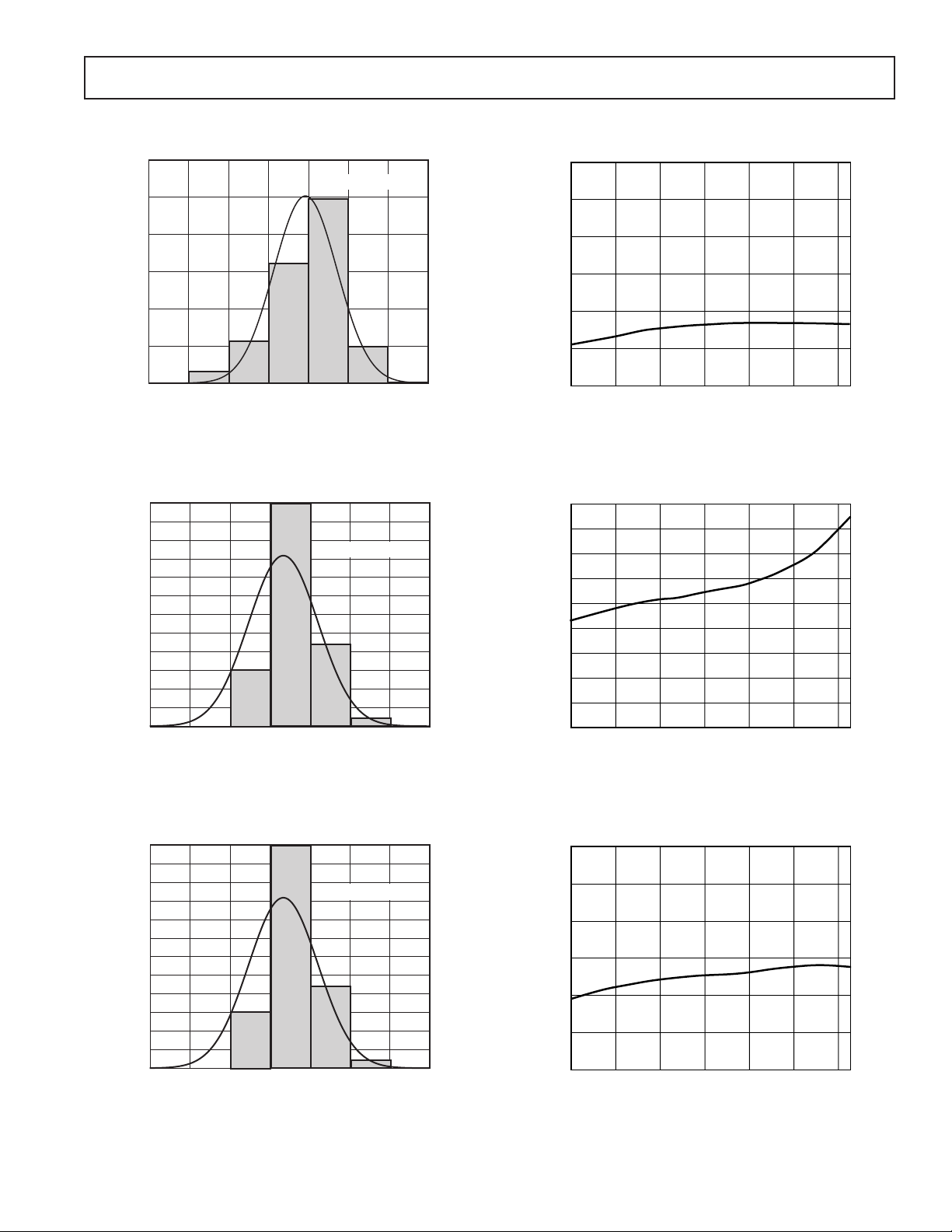
TPC 1. Gain Histogram f
60
55
50
45
40
35
30
25
PERCENTAGE
20
15
10
5
0
3.24
3.26 3.28 3.30 3.32 3.34 3.36 3.38
CONVERSION GAIN – dB
= 400 MHz, f
IN
INPUT 1dB COMPRESSION POINT – dBm
= 400 MHz, f
IN
MEAN: 5.57dB
OUT
MEAN: 3.31dBm
= 70 MHz, fLO = 330 MHz [Figure 24, Tables III and IV])
OUT
= 70 MHz
10
9
8
7
6
CONVERSION GAIN – dB
5
4
–40
0 20406080–20
TEMPERATURE – C
TPC 4. Gain Performance Over Temperature
= 400 MHz, f
f
IN
24
23
22
21
20
19
INPUT IP3 – dBm
18
17
16
15
–40
= 70 MHz
OUT
0 20406080–20
TEMPERATURE – C
TPC 2. Input IP3 Histogram fIN = 400 MHz,
f
= 70 MHz
OUT
60
55
50
45
40
35
30
25
PERCENTAGE
20
15
10
5
0
3.24
3.26 3.28 3.30 3.32 3.34 3.36 3.38
INPUT 1dB COMPRESSION POINT – dBm
MEAN: 3.31dBm
TPC 3. Input 1 dB Compression Point Histogram
= 400 MHz, f
f
IN
= 70 MHz
OUT
REV. A
TPC 5. Input IP3 Performance Over Temperature
= 400 MHz, f
f
IN
5.0
4.5
4.0
3.5
3.0
2.5
INPUT 1dB COMPRESSION POINT – dBm
2.0
–40
= 70 MHz
OUT
0 20406080–20
TEMPERATURE – C
TPC 6. Input 1 dB Compression Point Performance Over
Temperature (f
= 400 MHz, f
IN
= 70 MHz)
OUT
–5–
AD8343
RECEIVER CHARACTERISTICS (fIN = 900 MHz, f
35
30
MEAN: 3.63dB
25
20
15
PERCENTAGE
10
5
0
3.40 3.50 3.55 3.60 3.65 3.70 3.75 3.80 3.85
3.45
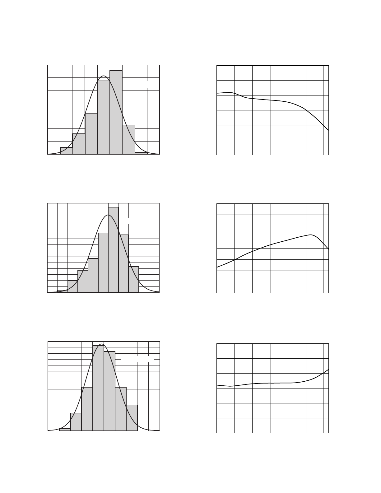
TPC 7. Gain Histogram fIN = 900 MHz, f
30
28
26
24
22
20
18
16
14
12
PERCENTAGE
10
8
6
4
2
0
18.4 18.6 18.8 19.0 19.2 19.4 19.6 19.8 20.0 20.2
18.2
CONVERSION GAIN – dB
INPUT IP3 – dBm
= 170 MHz
OUT
MEAN: 19.4dBm
= 170 MHz, fLO = 730 MHz [Figure 24, Tables III and IV])
OUT
6
5
4
3
2
CONVERSION GAIN – dB
1
0
–40
0 20406080–20
TEMPERATURE – C
TPC 10. Gain Performance Over Temperature
f
20.4
= 900 MHz, f
IN
23
22
21
20
19
18
INPUT IP3 – dBm
17
16
15
–40
= 170 MHz
OUT
0 20406080–20
TEMPERATURE – C
TPC 8. Input IP3 Histogram fIN = 900 MHz, f
30
28
26
24
22
20
18
16
14
12
PERCENTAGE
10
9
6
4
2
0
3.52
3.54 3.56 3.58 3.60 3.62 3.64 3.66 3.68 3.70 3.72
INPUT 1dB COMPRESSION POINT – dBm
OUT
MEAN: 3.62dBm
TPC 9. Input 1 dB Compression Point Histogram
= 900 MHz, f
f
IN
= 170 MHz
OUT
= 170 MHz
–6–
TPC 11. Input IP3 Performance Over Temperature
= 900 MHz, f
f
IN
5.0
4.5
4.0
3.5
3.0
2.5
INPUT 1dB COMPRESSION POINT – dBm
2.0
–40
= 170 MHz
OUT
0 20406080–20
TEMPERATURE – C
TPC 12. Input 1 dB Compression Point Performance
Over Temperature f
= 900 MHz, f
IN
= 170 MHz
OUT
REV. A
AD8343
TEMPERATURE – C
10
4
–40
CONVERSION GAIN – dB
9
8
7
6
5
0 20406080–20
TEMPERATURE – C
18
–40
INPUT IP3 – dBm
17
16
15
14
13
0 20406080–20
12
11
10
TEMPERATURE – C
5.0
2.0
–40
INPUT 1dB COMPRESSION POINT – dBm
4.5
4.0
3.5
3.0
2.5
0 20406080–20
RECEIVER CHARACTERISTICS (fIN = 1900 MHz, f
28
26
24
22
20
18
16
14
12
PERCENTAGE
10
8
6
4
2
0
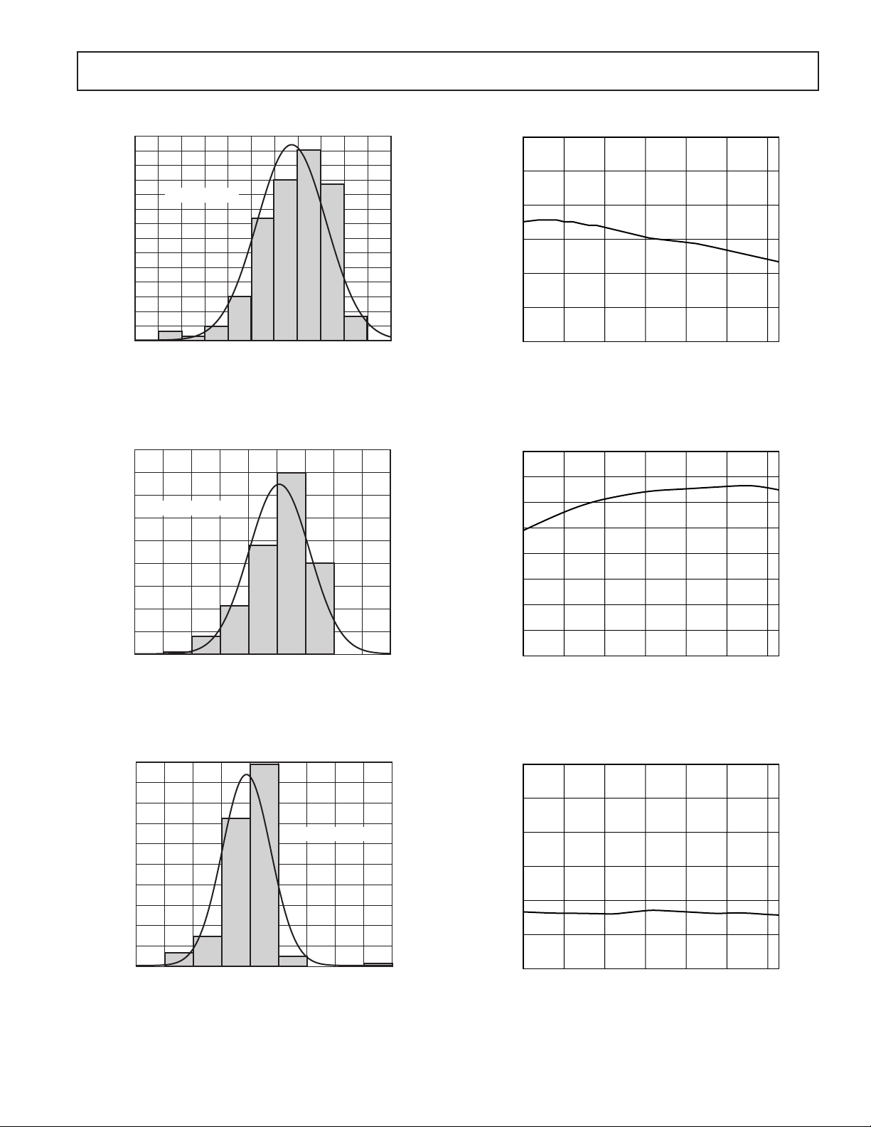
TPC 13. Gain Histogram fIN = 1900 MHz, f
45
40
35
30
25
20
PERCENTAGE
15
10
5
0
14.0
MEAN: 7.09dB
6.75
6.80
6.906.85 7.006.95 7.107.05 7.207.15 7.307.25
CONVERSION GAIN – dB
MEAN: 16.54dBm
14.5 15.0 15.5 16.0 16.5 17.0 17.5 18.0
INPUT IP3 – dBm
= 170 MHz
OUT
= 170 MHz, fLO = 1730 MHz [Figure 24, Tables III and IV])
OUT
TPC 16. Gain Performance Over Temperature
18.5
= 1900 MHz, f
f
IN
= 170 MHz
OUT
TPC 14. Input IP3 Histogram fIN = 1900 MHz,
= 170 MHz
f
OUT
50
45
40
35
30
25
20
PERCENTAGE
15
10
5
0
2.60
2.65 2.70 2.75 2.80 2.85 2.90 2.95 3.00 3.05
INPUT 1dB COMPRESSION POINT – dBm
MEAN: 2.8dBm
TPC 15. Input 1 dB Compression Point Histogram
= 1900 MHz, f
f
IN
= 170 MHz
OUT
REV. A
TPC 17. Input IP3 Performance Over Temperature
= 1900 MHz, f
f
IN
= 170 MHz
OUT
TPC 18. Input 1 dB Compression Point Performance
Over Temperature f
= 1900 MHz, f
IN
OUT
–7–
= 170 MHz
AD8343
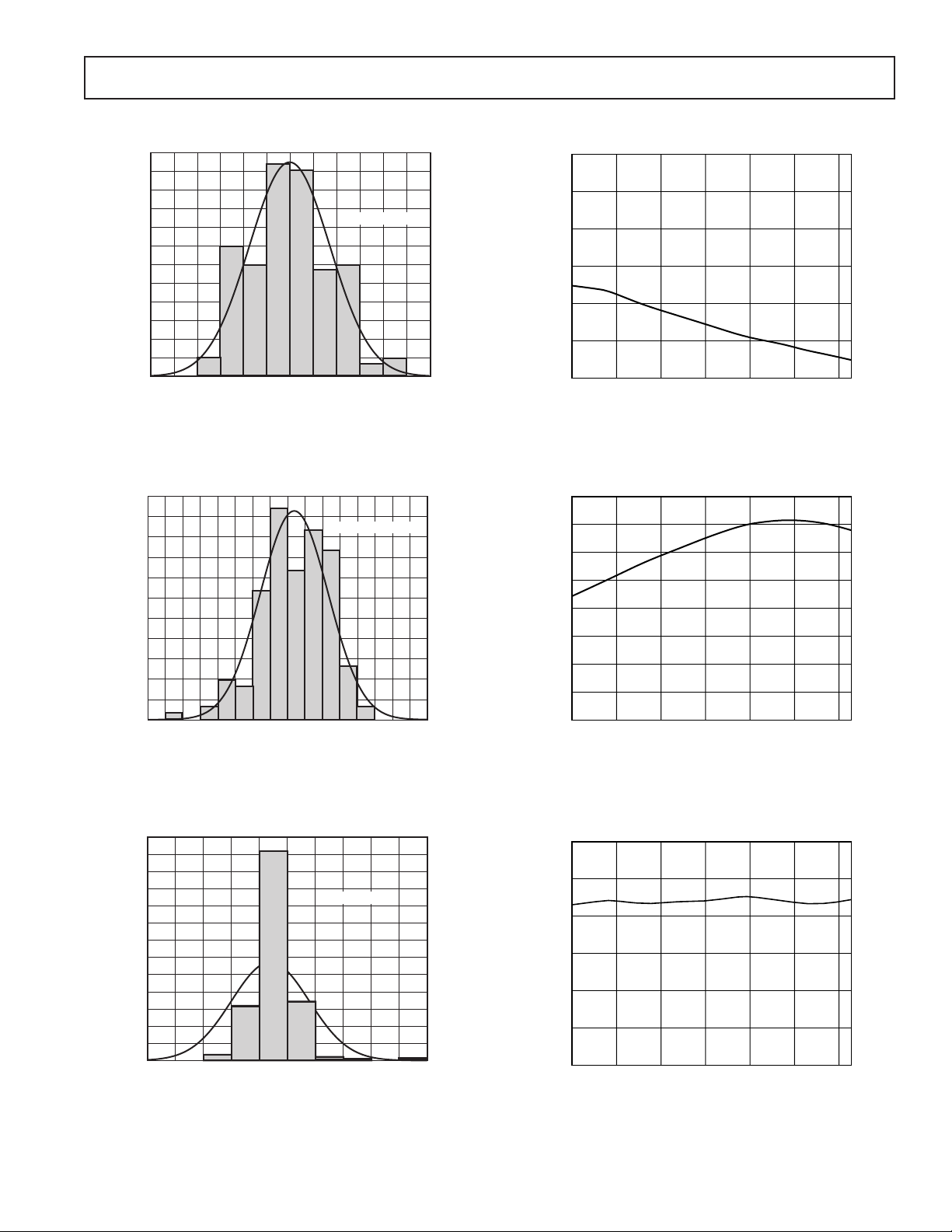
RECEIVER CHARACTERISTICS (fIN = 2400 MHz, f
40
35
30
25
20
15
PERCENTAGE
10
5
0
5.8 6.2 6.4 6.6 6.8 7.0 7.2 7.4 7.6
6.0
CONVERSION GAIN – dB
TPC 19. Gain Histogram fIN = 2400 MHz, f
35
30
25
20
15
PERCENTAGE
10
MEAN: 14.46dBm
5
0
13.0
13.2 13.4 13.6 13.8 14.0 14.2 14.4 14.6 14.8 15.0 15.2 15.4 15.6
INPUT IP3 – dBm
TPC 20. Input IP3 Histogram fIN = 2400 MHz, f
MEAN: 6.79dB
= 170 MHz
OUT
= 170 MHz
OUT
= 170 MHz, fLO = 2230 MHz [Figure 24, Tables III and IV])
OUT
10
9
8
7
6
CONVERSION GAIN – dB
5
4
–40
0 20406080–20
TEMPERATURE – C
TPC 22. Gain Performance Over Temperature
f
= 2400 MHz, f
IN
18
17
16
15
14
13
INPUT IP3 – dBm
12
11
10
–40
= 170 MHz
OUT
0 20406080–20
TEMPERATURE – C
TPC 23. Input IP3 Performance Over Temperature
= 2400 MHz, f
f
IN
= 170 MHz
OUT
45
40
35
30
25
20
PERCENTAGE
15
10
5
0
1.90
1.95 2.00 2.05 2.10 2.15 2.20 2.25 2.30 2.35 2.40
INPUT 1dB COMPRESSION POINT – dBm
INPUT: 2.11dBm
TPC 21. Input 1 dB Compression Point Histogram
= 2400 MHz, f
f
IN
= 170 MHz
OUT
3.0
2.5
2.0
1.5
1.0
0.5
INPUT 1dB COMPRESSION POINT – dBm
0
–40
0 20406080–20
TEMPERATURE – C
TPC 24. Input 1 dB Compression Point Performance Over
Temperature f
= 2400 MHz, f
IN
= 170 MHz
OUT
–8–
REV. A
AD8343
TEMPERATURE – C
10
4
–40
CONVERSION GAIN – dB
9
8
7
6
5
0 20406080–20
TEMPERATURE – C
18
–40
INPUT IP3 – dBm
17
16
15
14
13
0 20406080–20
12
11
10
TEMPERATURE – C
3.0
0
–40
INPUT 1dB COMPRESSION POINT – dBm
2.5
2.0
1.5
1.0
0.5
0 20406080–20
RECEIVER CHARACTERISTICS (fIN = 2400 MHz, f
24
22
20
18
16
14
12
10
PERCENTAGE
8
6
4
2
0
4.4
4.2 4.6 4.8 5.0 5.2 5.4 5.6 5.8 6.0 6.6
CONVERSION GAIN – dB
TPC 25. Gain Histogram fIN = 2400 MHz, f
22
20
18
16
14
12
10
PERCENTAGE
8
6
4
2
0
14.2
15.4 15.6 15.8 16.0 16.2 16.4 16.6 16.8 17. 2 17.4 17.6 17.8
INPUT IP3 – dBm
MEAN: 5.40dB
6.2 6.4
= 425 MHz
OUT
MEAN: 16.50dBm
17.0 18.015.215.0
= 425 MHz, fLO = 1975 MHz [Figure 24, Tables III and IV])
OUT
TPC 28. Gain Performance Over Temperature
f
= 2400 MHz, f
IN
= 425 MHz
OUT
TPC 26. Input IP3 Histogram fIN = 2400 MHz,
= 425 MHz
f
OUT
65
60
55
50
45
40
35
30
25
PERCENTAGE
20
15
10
5
0
2.05
2.00 2.10 2.15 2.20 2.25 2.30 2.35 2.40 2.45 2.50
INPUT 1dB COMPRESSION POINT – dBm
MEAN: 2.22dBm
TPC 27. Input 1 dB Compression Point Histogram
f
= 2400 MHz, f
IN
= 425 MHz
OUT
REV. A
TPC 29. Input IP3 Performance Over Temperature
f
= 2400 MHz, f
IN
= 425 MHz
OUT
TPC 30. Input 1 dB Compression Point Performance Over
Temperature f
= 2400 MHz, f
IN
= 425 MHz
OUT
–9–
 Loading...