ANALOG DEVICES AD828 Service Manual

Dual, Low Power
0.04
15
0.07
0.05
0.06
510
0.03
0.01
0.02
SUPPLY VOLTAGE – V
DIFFERENTIAL PHASE – Degrees
DIFFERENTIAL GAIN – Percent
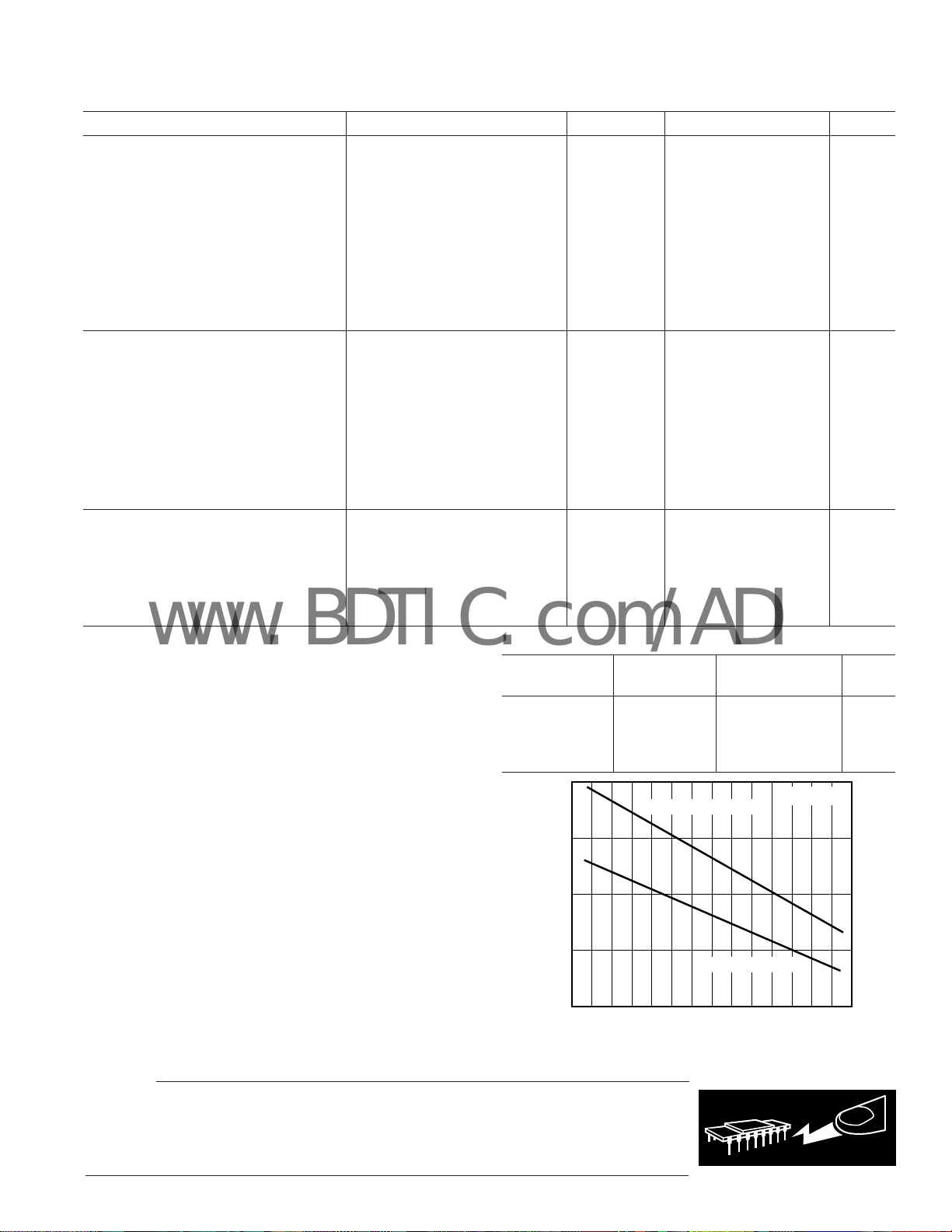
DIFF GAIN
DIFF PHASE
www.BDTIC.com/ADI
a
FEATURES
Excellent Video Performance
Differential Gain and Phase Error of 0.01% and 0.05
High Speed
130 MHz 3 dB Bandwidth (G = +2)
450 V/s Slew Rate
80 ns Settling Time to 0.01%
Low Power
15 mA Max Power Supply Current
High Output Drive Capability
50 mA Minimum Output Current per Amplifier
Ideal for Driving Back Terminated Cables
Flexible Power Supply
Specified for +5 V, 5 V, and 15 V Operation
3.2 V Min Output Swing into a 150 Load
= 5 V)
(V
S
Excellent DC Performance
2.0 mV Input Offset Voltage
Available in 8-Lead SOIC and 8-Lead Plastic Mini-DIP
GENERAL DESCRIPTION
The AD828 is a low cost, dual video op amp optimized for use
in video applications that require gains of +2 or greater and
high output drive capability, such as cable driving. Due to its
low power and single-supply functionality, along with excellent
differential gain and phase errors, the AD828 is ideal for powersensitive applications such as video cameras and professional
video equipment.
With video specs like 0.1 dB flatness to 40 MHz and low
differential gain and phase errors of 0.01% and 0.05°, along
with 50 mA of output current per amplifier, the AD828 is an
excellent choice for any video application. The 130 MHz gain
bandwidth and 450 V/µs slew rate make the AD828 useful in
many high speed applications, including video monitors, CATV,
color copiers, image scanners, and fax machines.
Video Op Amp
AD828
FUNCTIONAL BLOCK DIAGRAM
1
OUT1
2
–IN1
3
+IN1
V–
4
AD828
The AD828 is fully specified for operation with a single 5 V
power supply and with dual supplies from ±5 V to ±15 V. This
power supply flexibility, coupled with a very low supply current
of 15 mA and excellent ac characteristics under all power supply
conditions, make the AD828 the ideal choice for many demanding yet power-sensitive applications.
The AD828 is a voltage feedback op amp that excels as a gain
stage (gains > +2) or active filter in high speed and video systems
and achieves a settling time of 45 ns to 0.1%, with a low input
offset voltage of 2 mV max.
The AD828 is available in low cost, small 8-lead plastic mini-DIP
and SOIC packages.
8
V+
OUT2
7
–IN2
6
+IN2
5
+V
0.1F
R
75
75
BT
R
T
75
Figure 2. Differential Phase vs. Supply Voltage
V
IN
1k
R
75
T
1/2
AD828
–V
0.1F
1k
Figure 1. Video Line Driver
REV. C
Information furnished by Analog Devices is believed to be accurate and
reliable. However, no responsibility is assumed by Analog Devices for its
use, nor for any infringements of patents or other rights of third parties that
may result from its use. No license is granted by implication or otherwise
under any patent or patent rights of Analog Devices.
One Technology Way, P.O. Box 9106, Norwood, MA 02062-9106, U.S.A.
Tel: 781/329-4700www.analog.com
Fax: 781/326-8703 © Analog Devices, Inc., 2002

AD828–SPECIFICATIONS
www.BDTIC.com/ADI
(@ TA = 25C, unless otherwise noted.)
Parameter Conditions V
S
Min Typ Max Unit
DYNAMIC PERFORMANCE
–3 dB Bandwidth Gain = +2 ±5 V 60 85 MHz
±15 V 100 130 MHz
0, +5 V 30 45 MHz
Gain = –1 ±5 V 35 55 MHz
±15 V 60 90 MHz
0, +5 V 20 35 MHz
Bandwidth for 0.1 dB Flatness Gain = +2 ±5 V 30 43 MHz
C
= 1 pF ± 15 V 30 40 MHz
C
0, +5 V 10 18 MHz
Gain = –1 ±5 V 15 25 MHz
C
= 1 pF ± 15 V 30 50 MHz
C
0, +5 V 10 19 MHz
Full Power Bandwidth
Slew Rate R
*
V
= 5 V p-p
OUT
R
= 500 Ω±5 V 22.3 MHz
LOAD
V
= 20 V p-p
OUT
R
= 1 kΩ±15 V 7.2 MHz
LOAD
= 1 kΩ±5 V 300 350 V/µs
LOAD
Gain = –1 ±15 V 400 450 V/µs
0, +5 V 200 250 V/µs
Settling Time to 0.1% –2.5 V to +2.5 V ±5 V 45 ns
0 V–10 V Step, A
= –1 ±15 V 45 ns
V
Settling Time to 0.01% –2.5 V to +2.5 V ±5 V 80 ns
0 V–10 V Step, AV = –1 ±15 V 80 ns
NOISE/HARMONIC PERFORMANCE
Total Harmonic Distortion FC = 1 MHz ±15 V –78 dB
Input Voltage Noise f = 10 kHz ±5 V, ± 15 V 10 nV/√Hz
Input Current Noise f = 10 kHz ±5 V, ± 15 V 1.5 pA/√Hz
Differential Gain Error NTSC ±15 V 0.01 0.02 %
(R
= 150 Ω) Gain = +2 ±5 V 0.02 0.03 %
L
0, +5 V 0.08 %
Differential Phase Error NTSC ±15 V 0.05 0.09 Degrees
(R
= 150 Ω) Gain = +2 ±5 V 0.07 0.1 Degrees
L
0, +5 V 0.1 Degrees
DC PERFORMANCE
Input Offset Voltage ±5 V, ± 15 V 0.5 2 mV
T
to T
MIN
MAX
Offset Drift 10 µV/°C
Input Bias Current ±5 V, ± 15 V 3.3 6.6 µA
T
MIN
T
MAX
Input Offset Current ±5 V, ± 15 V 25 300 nA
T
to T
MIN
MAX
Offset Current Drift 0.3 nA/°C
Open-Loop Gain V
= ±2.5 V ±5 V
OUT
R
= 500 Ω 35 V/mV
LOAD
to T
T
R
V
R
T
V
R
MIN
LOAD
OUT
LOAD
MIN
OUT
LOAD
MAX
= 150 Ω 24 V/mV
= ±10 V ±15 V
= 1 kΩ 5.5 9 V/mV
to T
MAX
= ±7.5 V ±15 V
= 150 Ω (50 mA Output) 3 5 V/mV
2 V/mV
2.5 V/mV
INPUT CHARACTERISTICS
Input Resistance 300 kΩ
Input Capacitance 1.5 pF
Input Common-Mode Voltage Range ±5 V +3.8 +4.3 V
–2.7 –3.4 V
±15 V +13 +14.3 V
–12 –13.4 V
0, +5 V +3.8 +4.3 V
+1.2 +0.9 V
Common-Mode Rejection Ratio V
= +2.5 V, T
CM
= ±12 V ±15 V 86 120 dB
V
CM
T
to T
MIN
MAX
MIN
to T
MAX
±5 V 82 100 dB
±15 V 84 100 dB
3mV
10 µA
4.4 µA
500 nA
REV. C–2–

2.0
0
–50 90
1.5
0.5
–30
1.0
50 703010–10 80–40 40 60200–20
AMBIENT TEMPERATURE – C
MAXIMUM POWER DISSIPATION – Watts
8-LEAD MINI-DIP PACKAGE
8-LEAD SOIC PACKAGE
TJ = 150C
AD828
www.BDTIC.com/ADI
Parameter Conditions V
S
OUTPUT CHARACTERISTICS
Output Voltage Swing R
= 500 Ω±5 V 3.3 3.8 ±V
LOAD
= 150 Ω±5 V 3.2 3.6 ±V
R
LOAD
R
= 1 kΩ±15 V 13.3 13.7 ± V
LOAD
R
= 500 Ω±15 V 12.8 13.4 ± V
LOAD
R
= 500 Ω 0, +5 V 3.5 ±V
LOAD
Output Current ±15 V 50 mA
±5 V 40 mA
0, +5 V 30 mA
Short Circuit Current ±15 V 90 mA
Output Resistance Open-Loop 8 Ω
MATCHING CHARACTERISTICS
Dynamic
Crosstalk f = 5 MHz ± 15 V –80 dB
Gain Flatness Match G = +1, f = 40 MHz ±15 V 0.2 dB
Skew Rate Match G = –1 ±15 V 10 V/µs
DC
Input Offset Voltage Match T
Input Bias Current Match T
Open-Loop Gain Match V
Common-Mode Rejection Ratio Match V
Power Supply Rejection Ratio Match ± 5 V to ±15 V, T
to T
MIN
MIN
O
CM
MAX
to T
MAX
= ±10 V, RL = 1 kΩ, T
= ±12 V, T
MIN
MIN
to T
MIN
to T
MAX
MAX
to T
±5 V, ± 15 V 0.5 2 mV
±5 V, ± 15 V 0.06 0.8 µA
±15 V 0.01 0.15 mV/V
MAX
±15 V 80 100 dB
POWER SUPPLY
Operating Range Dual Supply ±2.5 ± 18 V
Single Supply +5 +36 V
Quiescent Current ±5 V 14.0 15 mA
T
to T
MIN
T
MIN
to T
MAX
MAX
Power Supply Rejection Ratio VS = ±5 V to ± 15 V, T
*Full power bandwidth = slew rate/2 π V
Specifications subject to change without notice.
PEAK
.
MIN
to T
±5 V 14.0 15 mA
±5 V 15 mA
MAX
ORDERING GUIDE
Temperature Package Package
Model Range Description Option
ABSOLUTE MAXIMUM RATINGS
Supply Voltage . . . . . . . . . . . . . . . . . . . . . . . . . . . . . . . . ±18 V
Internal Power Dissipation
2
1
Plastic DIP (N) . . . . . . . . . . . . . . . . . . See Derating Curves
AD828AN –40°C to +85°C 8-Lead Plastic DIP N-8
AD828AR –40°C to +85°C 8-Lead Plastic SOIC SO-8
AD828AR-REEL7 –40°C to +85°C 7" Tape and Reel SO-8
AD828AR-REEL –40°C to +85°C 13" Tape and Reel SO-8
Small Outline (R) . . . . . . . . . . . . . . . . . See Derating Curves
Input Voltage (Common Mode) . . . . . . . . . . . . . . . . . . . . ±V
S
Differential Input Voltage . . . . . . . . . . . . . . . . . . . . . . . . ± 6 V
Output Short Circuit Duration . . . . . . . . See Derating Curves
Storage Temperature Range (N, R) . . . . . . . . –65°C to +125°C
Operating Temperature Range . . . . . . . . . . . .–40°C to +85°C
Lead Temperature Range (Soldering 10 sec) . . . . . . . . +300°C
NOTES
1
Stresses above those listed under Absolute Maximum Ratings may cause permanent damage to the device. This is a stress rating only; functional operation of the
device at these or any other conditions above those indicated in the operational
section of this specification is not implied. Exposure to absolute maximum rating
conditions for extended periods may affect device reliability.
2
Specification is for device in free air:
8-Lead Plastic DIP Package: θJA = 100°C/W
8-Lead SOIC Package: θJA = 155°C/W
Figure 3. Maximum Power Dissipation vs.
Temperature for Different Package Types
CAUTION
ESD (electrostatic discharge) sensitive device. Electrostatic charges as high as 4000 V readily
accumulate on the human body and test equipment and can discharge without detection. Although
the AD828 features proprietary ESD protection circuitry, permanent damage may occur on devices
subjected to high energy electrostatic discharges. Therefore, proper ESD precautions are
recommended to avoid performance degradation or loss of functionality.
REV. C
–3–
Min Typ Max Unit
1.5
80 100 dB
80 90 dB
WARNING!
ESD SENSITIVE DEVICE

AD828
www.BDTIC.com/ADI
—Typical Performance Characteristics
20
15
+V
CM
10
–V
CM
5
INPUT COMMON-MODE RANGE – V
0
020
5
SUPPLY VOLTAGE – V
10
15
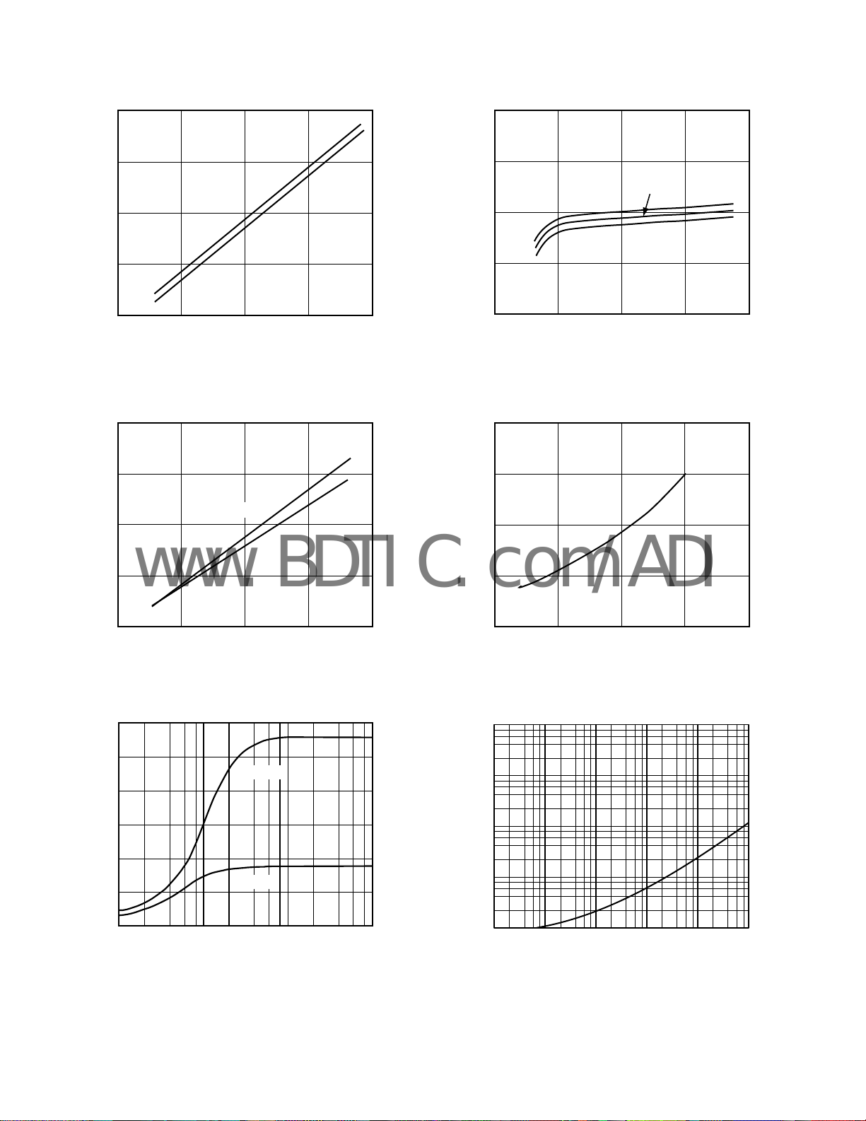
TPC 1. Common-Mode Voltage Range vs. Supply
Voltage
20
15
RL = 500
10
RL = 150
5
OUTPUT VOLTAGE SWING – V
7.7
7.2
+85C
6.7
–40C
6.2
QUIESCENT SUPPLY CURRENT PER AMP – mA
5.7
020
5
SUPPLY VOLTAGE – V
10
+25C
15
TPC 4. Quiescent Supply Current per Amp vs. Supply
Voltage for Various Temperatures
500
450
400
SLEW RATE – V/s
350
0
020
5
SUPPLY VOLTAGE – V
10
15
TPC 2. Output Voltage Swing vs. Supply Voltage
30
25
20
15
10
OUTPUT VOLTAGE SWING – V p-p
5
0
10
100
Vs = 15V
Vs = 5V
1k
LOAD RESISTANCE –
10k
TPC 3. Output Voltage Swing vs. Load Resistance
300
TPC 5. Slew Rate vs. Supply Voltage
100
10
1
0.1
CLOSED-LOOP OUTPUT IMPEDANCE –
0.01
1k 100M10k
TPC 6. Closed-Loop Output Impedance vs. Frequency
SUPPLY VOLTAGE – V
100k 1M
FREQUENCY – Hz
20501510
10M
REV. C–4–
 Loading...