High Common-Mode Voltage, Single Supply
–IN
GND
A1
A2
+IN
NC
+V
S
OUT
AD8200
5V
OUTPUT
INDUCTIVE
LOAD
4 TERM
SHUNT
CLAMP
DIODE
BATTERY 14V
POWER
DEVICE
COMMON NC = NO CONNECT
a
FEATURES
High Common-Mode Voltage Range –2 V to +24 V at a
5 V Supply Voltage
Operating Temperature Range
Die: –40C to +150C
8-Lead SOIC: –40C to +125C
Supply Voltage Range: 4.7 V to 12 V
Low-Pass Filter (One Pole or Two Pole)
EXCELLENT AC AND DC PERFORMANCE
15 V/C Max Offset Drift
20 ppm/C Max Gain Drift
80 dB CMRR Min DC to 10 kHz
PLATFORMS
Transmission Control
Diesel Injection Control
Engine Management
Semi-Active Suspension Control
Vehicle Dynamics Control
+IN
–IN
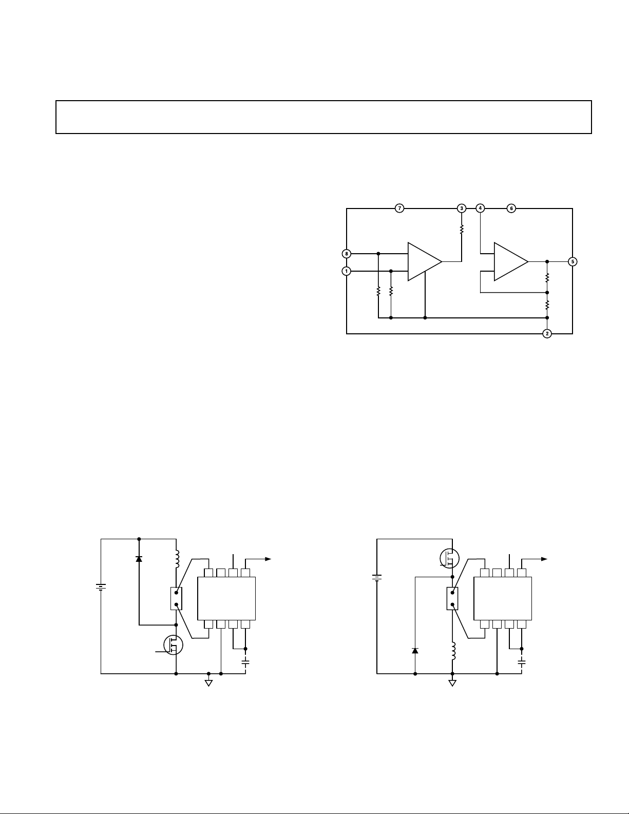
FUNCTIONAL BLOCK DIAGRAM
NC A1 A2
200k200k
NC = NO CONNECT
Difference Amplifier
AD8200
SOIC (R) Package
DIE Form
+V
S
AD8200
10k
10k
GND
G = X10
+IN
A1
–IN
100k
G = X2
+IN
A2
–IN
OUT
GENERAL DESCRIPTION
The AD8200 is a single-supply difference amplifier for amplifying
and low-pass filtering small differential voltages in the presence
of a large common-mode voltage. The input CMV range extends
from –2 V to +24 V at a typical supply voltage of 5 V.
The AD8200 is offered in die and packaged form. Both package
options are specified over wide temperature ranges, making the
AD8200 well suited for use in many automotive platforms. The
SOIC package is specified over a temperature range of –40°C to
+125°C. The die is specified from –40°C to +150°C.
BATTERY
INDUCTIVE
CLAMP
DIODE
14V
4 TERM
SHUNT
POWER
DEVICE
COMMON NC = NO CONNECT
LOAD
+IN
AD8200
–IN
NC
GND
5V
+V
OUT
S
A1
OUTPUT
A2
Figure 1. High-Line Current Sensor
REV. 0
Information furnished by Analog Devices is believed to be accurate and
reliable. However, no responsibility is assumed by Analog Devices for its
use, nor for any infringements of patents or other rights of third parties
which may result from its use. No license is granted by implication or
otherwise under any patent or patent rights of Analog Devices.
Automotive platforms demand precision components for better
system control. The AD8200 provides excellent ac and dc performance that keeps errors to a minimum in the user’s system.
Typical offset and gain drift in the SOIC package are 6 µV/°C
and 10 ppm/°C, respectively. The device also delivers a minimum CMRR of 80 dB from dc to 10 kHz.
The AD8200 features an externally accessible 100 kΩ resistor at
the output of the preamp A1, which can be used for low-pass
filter applications, and for establishing gains other than 20.
Figure 2. Low-Line Current Sensor
One Technology Way, P.O. Box 9106, Norwood, MA 02062-9106, U.S.A.
Tel: 781/329-4700 World Wide Web Site: http://www.analog.com
Fax: 781/326-8703 © Analog Devices, Inc., 2000

AD8200–SPECIFICATIONS
SINGLE SUPPLY
(TA = 25C, VS = 5 V, VCM = 0 V, RL = 10 k, Pin 5 to ground, unless otherwise noted.)
AD8200 SOIC AD8200 DIE
Parameter Condition Min Typ Max Min Typ Max Unit
SYSTEM GAIN
Initial 20 20
Error V
≥ 0.1 V dc –1 +1 –1 +1 %
O
vs. Temperature 10 20 25 30 ppm/°C
OFFSET VOLTAGE
Offset Voltage (RTI) VCM = 0.15 V –1 +1 –1 +1 mV
vs. Temperature 6 15 12 25 µV/°C
INPUT
Input Impedance
Differential 320 400 480 320 400 480 kΩ
Common-Mode 160 200 240 160 200 240 kΩ
CMV Continuous –2 +24 –2 +24 V
Common-Mode Rejection
1
VCM = 10 V
f = 1 kHz 80 80 dB
f = 10 kHz
2
80 80 dB
PREAMPLIFIER
Gain 10 10
Gain Error –1 +1 –1 +1 %
Output Voltage Range 0.02 4.8 0.02 4.8 V
Output Resistance 97 100 103 97 100 103 kΩ
OUTPUT BUFFER
Gain 2 2
Gain Error –1 +1 –1 +1 %
Output Voltage Range 0.02 4.8 0.02 4.8 V
Output Resistance 2 2 Ω
DYNAMIC RESPONSE
3 dB Bandwidth 30 50 30 50 kHz
Slew Rate 0.22 0.22 V/µs
NOISE
0.1 Hz to 10 Hz 10 10 µV p-p
Spectral Density, 1 kHz, RTI 300 300 nV/√Hz
POWER SUPPLY
Operating Range 4.7 12 4.7 12 V
Quiescent Current vs. Temp V
= 0.1 V dc 0.25 1 0.25 1 mA
O
PSRR VS = 4.7 V to 12 V 75 80 75 80 dB
TEMPERATURE RANGE
For Specified Performance –40 +125 –40 +150 °C
NOTES
1
Source Imbalance < 2 Ω.
2
The AD8200 preamplifier exceeds 80 dB CMRR at 10 kHz. However, since the signal is available only by way of a 100 k Ω resistor, even the small amounts of pinto-pin capacitance between Pins 1, 8 and 3, 4 may couple an input common-mode signal larger than the greatly attenuated preamplifier output. The effect of pin-topin coupling may be neglected in all applications using filter capacitors at Node 3.
Specifications subject to change without notice.
–2–
REV. 0

AD8200
ABSOLUTE MAXIMUM RATINGS*
PIN CONFIGURATION
Supply Voltage . . . . . . . . . . . . . . . . . . . . . . . . . . . . . . . 12.5 V
Transient Input Voltage (300 ms) . . . . . . . . . . . . . . . . . . 44 V
Continuous Input Voltage . . . . . . . . . . . . . . . . . . . . . . . . 35 V
Reversed Supply Voltage Protection . . . . . . . . . . . . . . . 0.3 V
Operating Temperature . . . . . . . . . . . (Die) – 40°C to +150°C
. . . . . . . . . (SOIC) –40°C to +125°C
Storage Temperature . . . . . . . . . . . . . . . . . . –65°C to +150°C
Output Short Circuit Duration . . . . . . . . . . . . . . . . Indefinite
1
–IN
2
GND
3
A1
(Not to Scale)
A2
4
NC = NO CONNECT
AD8200
TOP VIEW
Lead Temperature Range (Soldering 60 sec) . . . . . . . . 300°C
*Stresses beyond those listed under Absolute Maximum Ratings may cause
permanent damage to the device. This is a stress rating only; the functional
operation of the device at these or any other conditions above those indicated in
the operational sections of this specification is not implied. Exposure to absolute
maximum rating conditions for extended periods may affect device reliability.
ORDERING GUIDE
Model Temperature Range Package Description Package Option
AD8200R –40°C to +125°C Plastic SOIC SO-8
AD8200CHIPS –40°C to +150°C DIE Form
CAUTION
ESD (electrostatic discharge) sensitive device. Electrostatic charges as high as 4000 V readily
accumulate on the human body and test equipment and can discharge without detection. Although
the AD8200 features proprietary ESD protection circuitry, permanent damage may occur on
devices subjected to high-energy electrostatic discharges. Therefore, proper ESD precautions are
recommended to avoid performance degradation or loss of functionality.
8
+IN
7
NC
6
+V
S
5
OUT
WARNING!
ESD SENSITIVE DEVICE
+IN
–IN 1
METALLIZATION PHOTOGRAPH
+V
S
6
8
2
GND
3
A1
OUT5
A24
REV. 0
–3–
 Loading...