ANALOG DEVICES AD8194 Service Manual

Buffered 2:1 TMDS Switch
A
VCCAV
FEATURES
2 inputs, 1 output HDMI/DVI high speed signal switch
Pin-to-pin compatible with the AD8193
Enables HDMI 1.3-compliant receiver
4 TMDS channels per input/output
Supports 250 Mbps to 2.25 Gbps data rates
Supports 25 MHz to 225 MHz pixel clocks
Fully buffered unidirectional inputs/outputs
Equalized inputs for operation with long HDMI cables
(20 m at 2.25 Gbps)
Matched 50 Ω input and output on-chip terminations
Low added jitter
Single-supply operation (3.3 V)
Standards compliant: HDMI receiver, DVI
32-lead, 5 mm × 5 mm, RoHS-compliant LFCSP
APPLICATIONS
Advanced television (HDTV) sets
Multiple input displays
Projectors
A/V receivers
Set-top boxes
S_SEL
VTTI
IP_A[3:0]
IN_A[3:0]
IP_B[3:0]
IN_B[3:0]
VTTI
SET-TOP BOX
with Equalization
AD8194
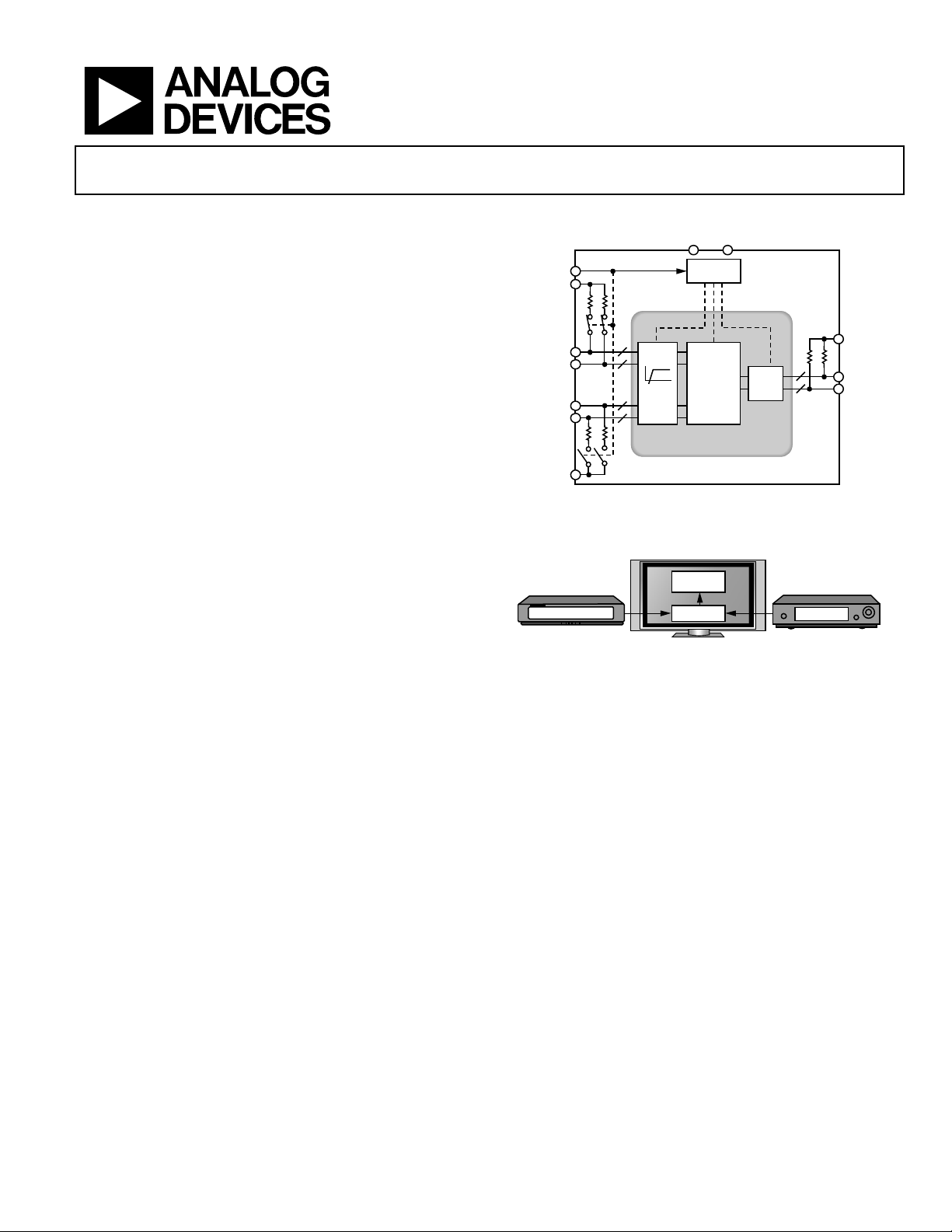
FUNCTIONAL BLOCK DIAGRAM
EE
CONTROL
LOGIC
+4
4
–
+
4
4
–
HIGH SPEED BUFFERED
EQ
SWITCH
CORE
Figure 1.
TYPICAL APPLICATION
HDTV SET
HDMI
RECEIVER
AD8194
Figure 2. Typical AD8194 Application for HDTV Sets
AD8194
Tx
4
4
DVD PLAYER
+
–
VTTO
OP[3:0]
ON[3:0]
07004-001
07004-002
GENERAL DESCRIPTION
The AD8194 is a low cost quad 2:1 TMDS® switch for high
speed HDMI™/DVI video applications. The AD8194 features
equalized inputs, ideal for systems with long cable runs. Its
primary function is to switch the high speed signals from one
of two single-link (HDMI or DVI) sources to the single-link
output. The AD8194 is a fully buffered switch solution with 50 Ω
input and output terminations, providing full-swing output
signal recovery and minimizing reflections for improved system
signal integrity.
The AD8194 is provided in a space-saving, 32-lead, LFCSP,
surface-mount, RoHS-compliant, plastic package and is specified
to operate over the −40°C to +85°C temperature range.
Rev. 0
Information furnished by Analog Devices is believed to be accurate and reliable. However, no
responsibility is assumed by Anal og Devices for its use, nor for any infringements of patents or ot her
rights of third parties that may result from its use. Specifications subject to change without notice. No
license is granted by implication or otherwise under any patent or patent rights of Analog Devices.
Trademarks and registered trademarks are the property of their respective owners.
PRODUCT HIGHLIGHTS
1. Data supports rates up to 2.25 Gbps, enabling greater than
1080p deep color (12-bit color) HDMI formats and greater
than UXGA (1600 × 2300) DVI resolutions.
2. Fully buffered inputs and outputs.
3. Input cable equalizer enables use of long cables at the
input. For a typical 24 AWG cable, the AD8194 compensates for more than 20 m at data rates up to 2.25 Gbps.
4. Matched 50 Ω on-chip input and output terminations
improve system signal integrity.
5. Single-pin source select bit.
6. Low added jitter.
One Technology Way, P.O. Box 9106, Norwood, MA 02062-9106, U.S.A.
Tel: 781.329.4700 www.analog.com
Fax: 781.461.3113 ©2007 Analog Devices, Inc. All rights reserved.

AD8194
TABLE OF CONTENTS
Features.............................................................................................. 1
Applications....................................................................................... 1
Functional Block Diagram .............................................................. 1
Typical Application........................................................................... 1
General Description ......................................................................... 1
Product Highlights ........................................................................... 1
Revision History ............................................................................... 2
Specifications..................................................................................... 3
Absolute Maximum Ratings............................................................ 4
Thermal Resistance ...................................................................... 4
Maximum Power Dissipation..................................................... 4
ESD Caution.................................................................................. 4
Pin Configuration and Function Descriptions............................. 5
REVISION HISTORY
11/07—Revision 0: Initial Version
Typical Performance Characteristics..............................................6
Theory of Operation .........................................................................9
Introduction...................................................................................9
Input Channels ..............................................................................9
Output Channels...........................................................................9
Switching Mode.......................................................................... 10
Application Notes........................................................................... 11
Switching High Speed Signals................................................... 11
Switching Low Speed Signals.................................................... 11
PCB Layout Guidelines.............................................................. 11
Outline Dimensions....................................................................... 16
Ordering Guide .......................................................................... 16
Rev. 0 | Page 2 of 16

AD8194
SPECIFICATIONS
TA = 27°C, AVCC = 3.3 V, VTTI = 3.3 V, VTTO = 3.3 V, AVEE = 0 V, differential input swing = 1000 mV, pattern = PRBS 27 − 1,
data rate = 2.25 Gbps, TMDS outputs terminated with external 50 Ω resistors to 3.3 V, unless otherwise noted.
Table 1.
Parameter Conditions/Comments Min Typ Max Unit
DYNAMIC PERFORMANCE
Maximum Data Rate (DR) per Channel NRZ 2.25 Gbps
Bit Error Rate (BER) 10−9
Added Deterministic Jitter 10 ps (p-p)
Added Random Jitter 1 ps (rms)
Differential Intrapair Skew At output 1 ps
Differential Interpair Skew
EQUALIZATION PERFORMANCE
Receiver Boost frequency = 1.125 GHz 12 dB
INPUT CHARACTERISTICS
Input Voltage Swing Differential 150 1200 mV
Input Common-Mode Voltage (V
OUTPUT CHARACTERISTICS
High Voltage Level Single-ended high speed channel AVCC mV
Low Voltage Level Single-ended high speed channel AVCC − 600 AVCC − 400 mV
Rise/Fall Time (20% to 80%) 75 178 ps
TERMINATION
Input Resistance Single-ended 50 Ω
Output Resistance Single-ended 50 Ω
POWER SUPPLY
AVCC Operating range 3 3.3 3.6 V
QUIESCENT CURRENT
AVCC 50 70 mA
VTTI 40 54 mA
VTTO 40 65 mA
POWER DISSIPATION
3
SOURCE SELECT INTERFACE
Input High Voltage (VIH) S_SEL 2 V
Input Low Voltage (VIL) S_SEL 0.8 V
1
Differential interpair skew is measured between the TMDS pairs of a single link.
2
Typical value assumes only the selected HDMI/DVI link is active with nominal signal swings and that the unselected HDMI/DVI link is deactivated. Minimum and
maximum limits are measured at the respective extremes of input termination resistance and input voltage swing.
3
The total power dissipation excludes power dissipated in the 50 Ω off-chip loads.
1
ICM
2
At output 30 ps
) AVCC − 800 AVCC mV
429 mW
Rev. 0 | Page 3 of 16

AD8194
ABSOLUTE MAXIMUM RATINGS
Table 2.
Parameter Rating
AVCC to AVEE 3.7 V
VTTI AVCC + 0.6 V
VTTO AVCC + 0.6 V
Internal Power Dissipation 1.2 W
High Speed Input Voltage AVCC − 1.4 V < VIN < AVCC + 0.6 V
High Speed Differential
Input Voltage
Source Select (S_SEL) AVEE − 0.3 V < VIN < AVCC + 0.6 V
Storage Temperature Range −65°C to +125°C
Operating Temperature
Range
Junction Temperature 150°C
2.0 V
−40°C to +85°C
Stresses above those listed under Absolute Maximum Ratings
may cause permanent damage to the device. This is a stress
rating only; functional operation of the device at these or any
other conditions above those indicated in the operational
section of this specification is not implied. Exposure to absolute
maximum rating conditions for extended periods may affect
device reliability.
THERMAL RESISTANCE
θJA is specified for the worst-case conditions: a device soldered
in a 4-layer JEDEC circuit board for surface-mount packages.
is specified for the exposed pad soldered to the circuit board
θ
JC
with no airflow.
Table 3. Thermal Resistance
θ
Package Type
32-Lead LFCSP 47 6.8 °C/W
θJC
JA
Unit
MAXIMUM POWER DISSIPATION
The maximum power that can be safely dissipated by the
AD8194 is limited by the associated rise in junction temperature. The maximum safe junction temperature for plastic
encapsulated devices is determined by the glass transition
temperature of the plastic, approximately 150°C. Temporarily
exceeding this limit may cause a shift in parametric performance
due to a change in the stresses exerted on the die by the package.
Exceeding a junction temperature of 175°C for an extended
period can result in device failure. To ensure proper operation,
it is necessary to observe the maximum power derating as
determined by the coefficients in
Tabl e 3.
ESD CAUTION
Rev. 0 | Page 4 of 16

AD8194
PIN CONFIGURATION AND FUNCTION DESCRIPTIONS
IP_A1
IN_A1
S_SEL
IP_A0
IN_A0
AVEE
IP_B3
32313029282726
PIN 1
IN_A2
IP_A2
VTTI
IN_A3
IP_A3
AVCC
OP3
ON3
NOTES
1. THE AD8194 LF CSP HAS AN EXPOSED PADDLE (ePAD) ON THE UNDERSIDE
OF THE PACKAG E, WHICH AI DS IN HEAT DI SSIPATI ON. THE ePAD MUST BE
ELECTRICAL LY CONNECTED TO THE AVEE SUPPLY PL ANE TO MEET
THERMAL SPECIFICATIONS.
INDICATO R
1
2
3
4
5
6
7
8
AD8194
TOP VIEW
(Not to Scale)
9
10111213141516
OP2
OP1
ON2
AVEE
Figure 3. Pin Configuration
IN_B3
25
24
IP_B2
23
IN_B2
22
AVCC
21
IP_B1
20
IN_B1
19
VTTI
18
IP_B0
17
IN_B0
OP0
ON1
ON0
VTTO
07004-003
Table 4. Pin Function Descriptions
Pin No. Mnemonic Type
1
Description
1 IN_A2 HS I High Speed Input Complement.
2 IP_A2 HS I High Speed Input.
3, 19 VTTI Power Input Termination Supply. Nominally connected to AVCC.
4 IN_A3 HS I High Speed Input Complement.
5 IP_A3 HS I High Speed Input.
6, 22 AVCC Power Positive Power Supply. 3.3 V nominal.
7 OP3 HS O High Speed Output.
8 ON3 HS O High Speed Output Complement.
9 OP2 HS O High Speed Output.
10 ON2 HS O High Speed Output Complement.
11, 27, ePAD AVEE Power Negative Power Supply. 0 V nominal.
12 OP1 HS O High Speed Output.
13 ON1 HS O High Speed Output Complement.
14 VTTO Power Output Termination Supply. Nominally connected to AVCC.
15 OP0 HS O High Speed Output.
16 ON0 HS O High Speed Output Complement.
17 IN_B0 HS I High Speed Input Complement.
18 IP_B0 HS I High Speed Input.
20 IN_B1 HS I High Speed Input Complement.
21 IP_B1 HS I High Speed Input.
23 IN_B2 HS I High Speed Input Complement.
24 IP_B2 HS I High Speed Input.
25 IN_B3 HS I High Speed Input Complement.
26 IP_B3 HS I High Speed Input.
28 IN_A0 HS I High Speed Input Complement.
29 IP_A0 HS I High Speed Input.
30 S_SEL Control Source Selector Pin.
31 IN_A1 HS I High Speed Input Complement.
32 IP_A1 HS I High Speed Input.
1
HS = high speed, I = input, O = output.
Rev. 0 | Page 5 of 16
 Loading...