Analog Devices AD8116JST, AD8116-EB Datasheet
200 MHz, 16 ⴛ 16 Buffered
a
FEATURES
Large 16 ⴛ 16 High Speed Nonblocking Switch Array
Switch Array Controllable via an 80-Bit Serial Word
Serial Data Out Allows “Daisy Chaining” of Multiple
AD8116s to Create Large Switch Arrays Over 256 ⴛ 256
Complete Solution
Buffered Inputs
16 Individual Output Amplifiers
Drives 150 ⍀ Loads
Excellent Video Performance
60 MHz 0.1 dB Gain Flatness
0.01% Differential Gain Error (R
0.01ⴗ Differential Phase Error (R
Excellent AC Performance
200 MHz –3 dB Bandwidth
300 V/s Slew Rate
Low Power of 900 mW (3.5 mW per Point)
Low All Hostile Crosstalk of –70 dB @ 5 MHz
Output Disable Allows Direct Connection of Multiple
Device Outputs
Chip Enable Allows Selection of Individual AD8116s in
Large Arrays (or Parallel Programming of AD8116s)
Reset Pin Allows Disabling of All Outputs (Connected
Through a Capacitor to Ground Provides “Power-
On” Reset Capability)
128-Lead LQFP Package (14 mm ⴛ 14 mm)
APPLICATIONS
Routing of High Speed Signals Including:
Composite Video (NTSC, PAL, S, SECAM, etc.)
Component Video (YUV, RGB, etc.)
3-Level Digital (HDB3)
Video on Demand
Ultrasound
Communication Satellites
PRODUCT DESCRIPTION
The AD8116 is a high speed 16 × 16 video crosspoint switch
matrix. It offers a –3 dB signal bandwidth greater than 200 MHz
and channel switch times of 60 ns with 0.1% settling. With –70 dB
of crosstalk and –105 dB of isolation (@ 5 MHz), the AD8116
is useful in many high speed applications. The differential gain
and differential phase errors of better than 0.01% and 0.01°,
respectively, along with 0.1 dB flatness out to 60 MHz make the
AD8116 ideal for video signal switching.
The AD8116 includes output buffers that can be placed into a
high impedance state for paralleling crosspoint outputs so that
off channels do not load the output bus. It operates on voltage
*Patent Pending.
REV. B
Information furnished by Analog Devices is believed to be accurate and
reliable. However, no responsibility is assumed by Analog Devices for its
use, nor for any infringements of patents or other rights of third parties that
may result from its use. No license is granted by implication or otherwise
under any patent or patent rights of Analog Devices.
= 150 ⍀)
L
= 150 ⍀)
L
Video Crosspoint Switch
AD8116*
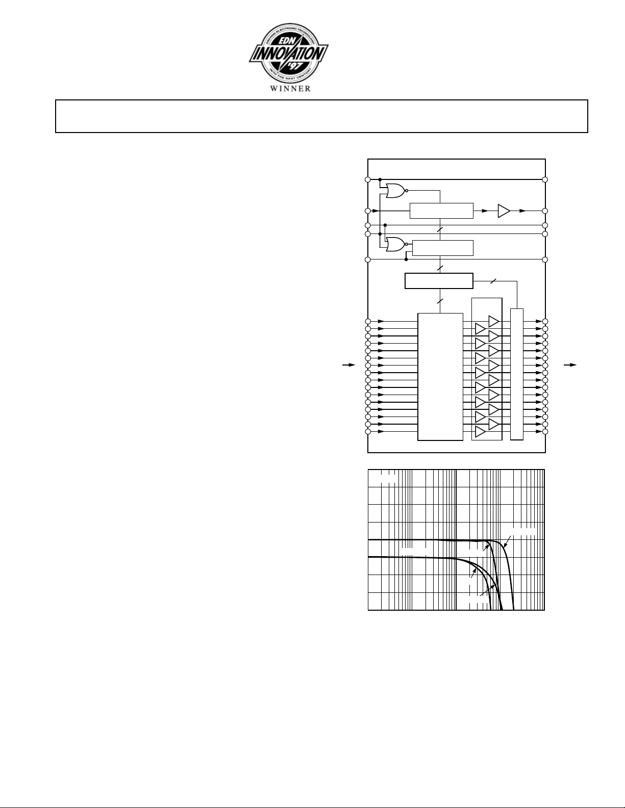
FUNCTIONAL BLOCK DIAGRAM
AD8116
CLK
DATA IN
UPDATE
CE
RESET
16 INPUTS
4
RL = 50⍀
3
2
1
0
–1
MAGNITUDE – dB
–2
–3
–4
100k
80-BIT SHIFT REG.
80
PARALLEL LATCH
80
DECODE
16 ⴛ 5:16 DECODERS
256
SWITCH
MATRIX
FLATNESS
FREQUENCY – Hz
16
OUTPUT
BUFFER
+1
+1
+1
+1
+1
+1
+1
+1
+1
+1
+1
+1
+1
+1
+1
+1
2V p-p
2V p-p
200mV p-p
10M 100M
ENABLE/DISABLE
200mV p-p
Figure 1. Frequency Response
supplies of ±5 V while consuming only 90 mA of idle current.
The channel switching is performed via a serial digital control
that can accommodate “daisy chaining” of several devices.
The AD8116 is packaged in a 128-lead LQFP package occupying only 0.36 square inches, and is specified over the commercial temperature range of 0°C to 70°C.
One Technology Way, P.O. Box 9106, Norwood, MA 02062-9106, U.S.A.
Tel: 781/329-4700 www.analog.com
Fax: 781/326-8703 © Analog Devices, Inc., 2001
CLK
DATA OUT
UPDATE
CE
RESET
SET INDIVIDUAL OR
RESET ALL OUTPUTS
TO "OFF"
16 OUTPUTS
0.5
0.4
0.3
0.2
0.1
0
0.1dB FLATNESS – dB
–0.1
–0.2
–0.3
1G1M

AD8116–SPECIFICATIONS
(VS = ⴞ5 V, TA = 25ⴗC, RL = 1 k⍀ unless otherwise noted.)
Limit Reference
Parameter Conditions Min Typ Max Unit Figure
DYNAMIC PERFORMANCE
–3 dB Bandwidth 200 mV p-p, R
1 V p-p, R
2 V p-p, R
Slew Rate 2 V Step, R
Settling Time 0.1%, 2 V Step, R
Gain Flatness 0.05 dB, 200 mV p-p, R
0.05 dB, 2 V p-p, R
0.1 dB, 200 mV p-p, R
= 150 Ω 200 MHz 1
L
= 150 Ω 120 MHz –
L
= 150 Ω 80 MHz 1
L
= 150 Ω 300 V/µs5
L
= 150 Ω 60 ns 6
L
= 150 Ω 25 MHz 1
L
= 150 Ω 20 MHz 1
L
= 150 Ω 60 MHz 1
L
0.1 dB, 2 V p-p, RL = 150 Ω 45 MHz 1
NOISE/DISTORTION PERFORMANCE
Differential Gain Error NTSC or PAL, RL = 1 kΩ 0.01 % –
NTSC or PAL, R
Differential Phase Error NTSC or PAL, R
NTSC or PAL, R
= 150 Ω 0.01 % –
L
= 1 kΩ 0.01 Degrees –
L
= 150 Ω 0.01 Degrees –
L
Crosstalk, All Hostile ƒ = 5 MHz –70 dB 2
ƒ = 10 MHz –60 dB 2
Off Isolation, Input-Output ƒ = 10 MHz, R
= 150 Ω, One Channel –105 dB 11
L
Input Voltage Noise 0.01 MHz to 50 MHz 15 nV/√Hz 8
DC PERFORMANCE
Gain No Load 0.995 0.999 1.000 V/V –
R
= 1 kΩ 0.992 0.999 1.000 V/V –
L
Gain Matching No Load, Ch-Ch 0.15 % –
RL = 1 kΩ, Ch-Ch 0.5 % –
OUTPUT CHARACTERISTICS
Output Offset Voltage Worst-Case All Switch Configurations 15 45 mV 17
Output Impedance DC, Enabled 0.2 Ω 12
Disabled 1 10 MΩ 9
Output Disable Capacitance 3 pF 9
Output Leakage Current Disabled 1 µA–
Output Voltage Range ±2.5 ±3V–
Output Current 20 40 mA –
Short Circuit Current 65 mA –
INPUT CHARACTERISTICS
Input Voltage Range ±2.5 ±3V–
Input Capacitance Any Switch Configuration 5 pF 13
Input Resistance 1 10 MΩ 13
Input Bias Current 25µA–
SWITCHING CHARACTERISTICS
Enable On Time 60 ns –
Switching Time 50% UPDATE to 1% Output Settling, 50 ns 16
2 V Step
Switching Transient (Glitch) 15 mV p-p 10
POWER SUPPLIES
Supply Current AVCC, Outputs Enabled, No Load 75 95 mA –
AVCC, Outputs Disabled 25 mA –
AVEE, Outputs Enabled, No Load 70 95 mA –
AVEE, Outputs Disabled 22.5 mA –
DVCC, Outputs Enabled, No Load 25 35 mA –
DVEE, Outputs Enabled, No Load 10 15 mA –
Supply Voltage Range ±4.5 to ±5.5 V –
PSRR ƒ = 100 kHz 60 dB 7
ƒ = 1 MHz 40 dB 7
OPERATING TEMPERATURE RANGE
Temperature Range Operating (Still Air) 0 to 70 °C–
θ
JA
Specifications subject to change without notice.
Operating (Still Air) 37 °C/W –
–2–
REV. B
AD8116
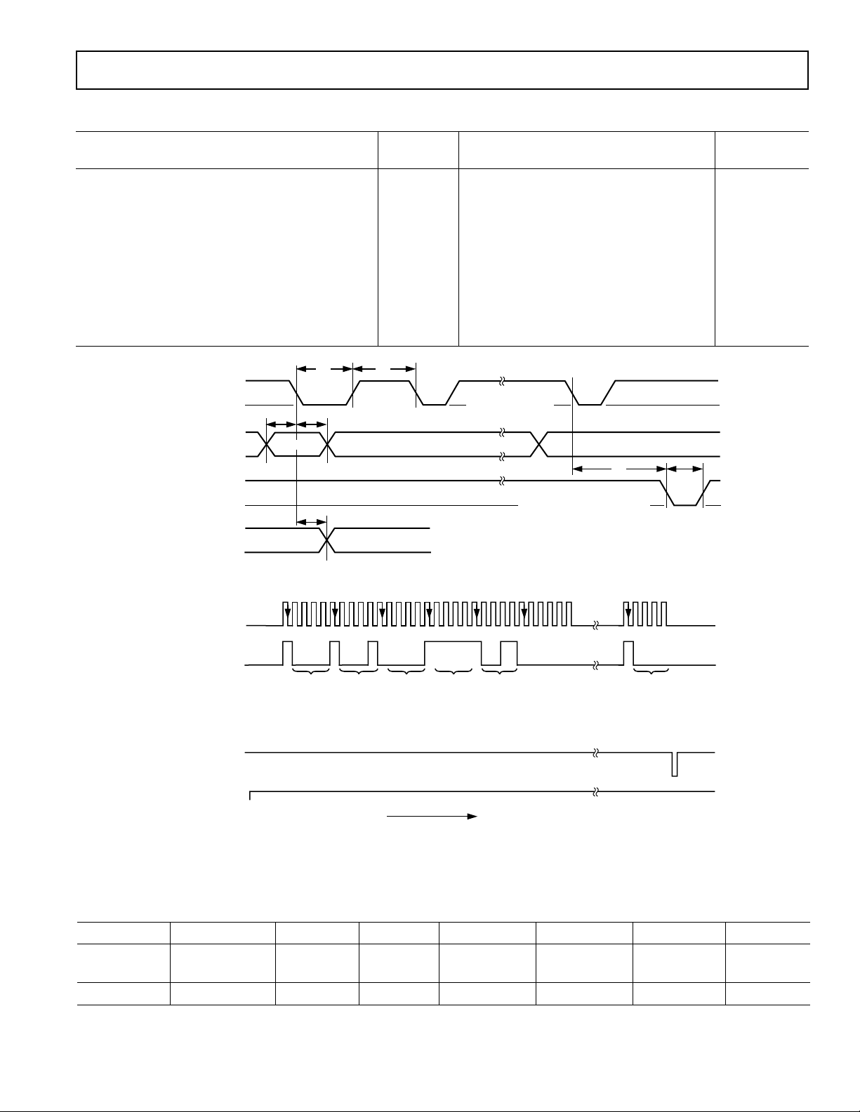
TIMING CHARACTERISTICS
Limit
Parameter Symbol Min Typ Max Unit
Data Setup Time t
CLK Pulsewidth t
Data Hold Time t
CLK Pulse Separation t
CLK to UPDATE Delay t
UPDATE Pulsewidth t
CLK to DATA OUT Valid t
1
2
3
4
5
6
7
Propagation Delay, UPDATE to Switch On or Off – 50 ns
Data Load Time, CLK = 5 MHz – 16 µs
CLK, UPDATE Rise and Fall Times – 100 ns
RESET Time – 200 ns
20 ns
100 ns
20 ns
100 ns
0ns
50 ns
200 ns
CLK
DATA IN
1 = LATCHED
UPDATE
0 = TRANSPARENT
DATA OUT
CLOCK
DATA IN
UPDATE
t
1
0
t1t
1
OUT15 (D4) OUT15 (D3) OUT00 (D0)
0
2
3
t
7
12 34 5 67 8910 15 20 25 75 79
0
NPUT 00
CONNECT TO
ENABLE OUTPUT 15
t
4
INPUT 01
CONNECT TO
ENABLE OUTPUT 14
DISABLE OUTPUT 13
DON’T CARE
ENABLE OUTPUT 12
LOAD DATA INTO
SERIAL REGISTER
ON FALLING EDGE
INPUT 15
CONNECT TO
CONNECT TO
ENABLE OUTPUT 11
TRANSFER DATA FROM SERIAL
REGISTER TO PARALLEL
LATCHES DURING LOW LEVEL
INPUT 03
t
5
CONNECT TO
ENABLE OUTPUT 00
INPUT 00
t
6
T = 0
INCREASING TIME
Figure 2. Timing Diagram and Programming Example
Table I. Logic Levels
V
IH
CLK, DATA IN, CLK, DATA IN, DATA OUT DATA OUT CLK, DATA IN, CLK, DATA IN, DATA OUT DATA OUT
CE, UPDATE CE, UPDATE CE, UPDATE CE, UPDATE
2.0 V min 0.8 V max 2.7 V min 0.5 V max 20 µA max –400 µA min –400 µA max 3.0 mA min
REV. B
V
IL
V
OH
V
OL
I
IH
I
IL
I
OH
I
OL
–3–
AD8116
ABSOLUTE MAXIMUM RATINGS
Supply Voltage . . . . . . . . . . . . . . . . . . . . . . . . . . . . . . . .12.0 V
Internal Power Dissipation
2
1
AD8116 128-Lead Plastic LQFP (ST) . . . . . . . . . . . . 3.5 W
Input Voltage . . . . . . . . . . . . . . . . . . . . . . . . . . . . . . . . . . ⫾V
S
Output Short Circuit Duration
. . . . . . . . . . . . . . . . . . . . Observe Power Derating Curves
Storage Temperature Range . . . . . . . . . . . . –65°C to +125°C
Lead Temperature Range (Soldering 10 sec) . . . . . . . . . 300°C
NOTES
1
Stresses above those listed under Absolute Maximum Ratings may cause perma-
nent damage to the device. This is a stress rating only; functional operation of the
device at these or any other conditions above those indicated in the operational
section of this specification is not implied. Exposure to absolute maximum rating
conditions for extended periods may affect device reliability.
2
Specification is for device in free air (TA = 25°C):
128-lead plastic LQFP (ST): θJA = 37°C/W.
ORDERING GUIDE
Temperature Package Package
Model Range Description Option
AD8116JST 0°C to 70°C 128-Lead Plastic LQFP ST-128A
(14 mm × 14 mm)
AD8116-EB Evaluation Board
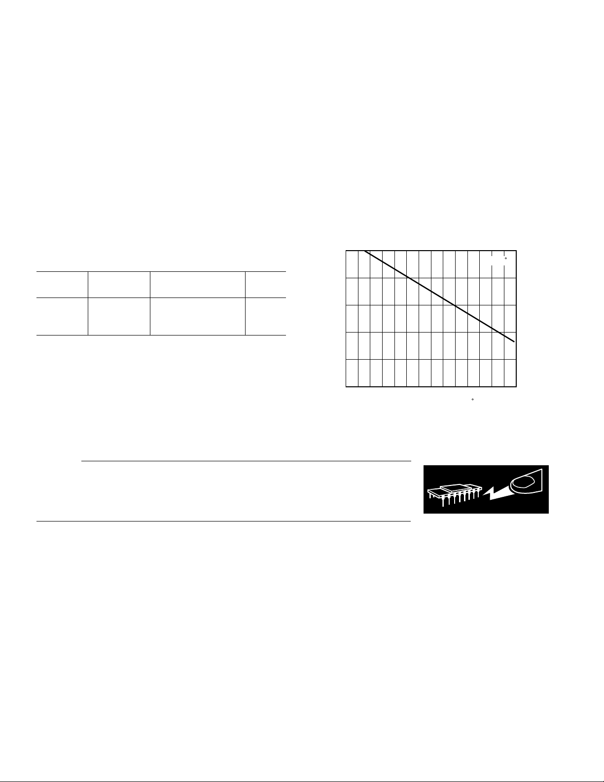
MAXIMUM POWER DISSIPATION
The maximum power that can be safely dissipated by the
AD8116 is limited by the associated rise in junction temperature. The maximum safe junction temperature for plastic
encapsulated devices is determined by the glass transition
temperature of the plastic, approximately 150°C. Temporarily
exceeding this limit may cause a shift in parametric performance
due to a change in the stresses exerted on the die by the package.
Exceeding a junction temperature of 175°C for an extended
period can result in device failure.
While the AD8116 is internally short circuit protected, this may
not be sufficient to guarantee that the maximum junction temperature (150°C) is not exceeded under all conditions. To
ensure proper operation, it is necessary to observe the maximum
power derating curves shown in Figure 3.
5.0
TJ = 150 C
4.0
3.0
2.0
1.0
MAXIMUM POWER DISSIPATION – Watts
0
–50 80–40 –30 –20 –10 0 10203040506070
AMBIENT TEMPERATURE – C
Figure 3. Maximum Power Dissipation vs. Temperature
CAUTION
ESD (electrostatic discharge) sensitive device. Electrostatic charges as high as 4000 V readily
accumulate on the human body and test equipment and can discharge without detection.
Although the AD8116 features proprietary ESD protection circuitry, permanent damage may
occur on devices subjected to high-energy electrostatic discharges. Therefore, proper ESD
precautions are recommended to avoid performance degradation or loss of functionality.
90
WARNING!
ESD SENSITIVE DEVICE
–4–
REV. B
AD8116
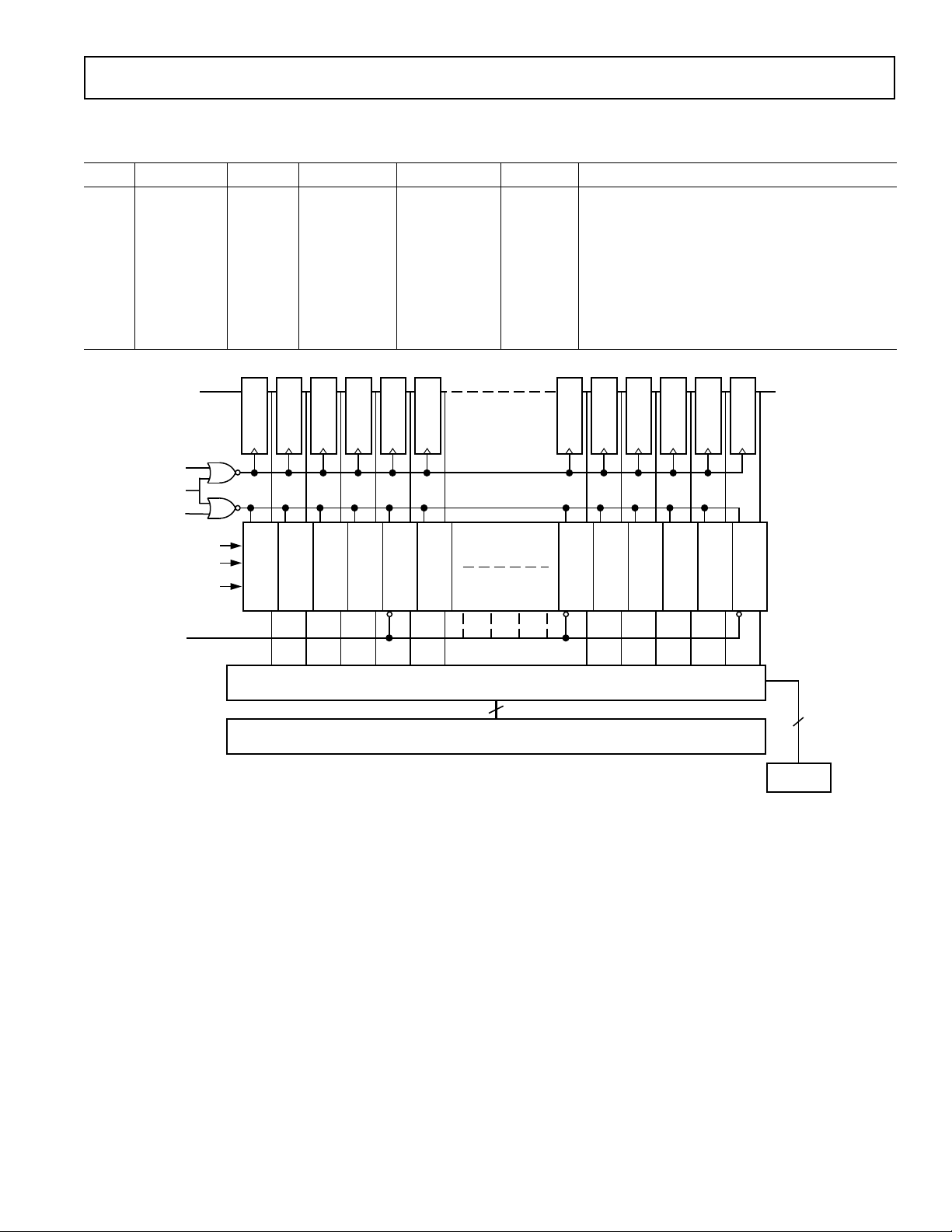
Table II. Operation Truth Table
Control Lines
CE UPDATE CLK DATA IN DATA OUT RESET Operation/Comment
1 X X X X 1 No change in logic.
01 f Data
i
0 0 X X X 1 Data in the serial shift register transfers into the
X X X X X 0 Asynchronous operation. All outputs are disabled.
Data
i-80
1 The data on the DATA IN line is loaded into the
serial register. The first bit clocked into the serial
register appears at DATA OUT 80 clocks later.
parallel latches that control the switch array.
Latches are transparent.
Remainder of logic is unchanged.
DATA IN
CLK
CE
UPDATE
OUTPUT CH
CH BIT #
SERIAL BIT #
RESET
DDDDDDQQQQQQ
CLK CLK CLK CLK CLK CLK
0
12 3EN
LSB
MSB
0
Figure 4. Logic Diagram
DECODE
256
SWITCH MATRIX
DDDDDDQQQQQQ
CLK CLK CLK CLK CLK CLK
LE D LE D LE D LE D LE D LE DLE D LE D LE D LE D LE D LE D
OUT14 OUT15 OUT15 OUT15 OUT15 OUT15OUT0 OUT0 OUT0 OUT0 OUT0 OUT1
EN 0
54 321 079 78 77 76 75 74
CLRQQQQQQCLRCLR Q QQQQQ
123EN
LSB
MSB
DATA OUT
16
OUTPUT
ENABLE
REV. B
–5–
AD8116
PIN FUNCTION DESCRIPTIONS
Pin Name Pin Numbers Pin Description
INxx 2, 4, 6, 8, 10, 12, 14, 16, 18, Analog Inputs; xx = Channel No. 00 thru 15.
20, 22, 24, 26, 28, 30, 32
DATA IN 37, 126 Serial Data Input, TTL Compatible.
CLK 36, 125 Serial Clock, TTL Compatible. Falling edge triggered.
DATA OUT 35, 124 Serial Data Out, TTL Compatible.
UPDATE 38, 123 Enable (Transparent) “Low.” Allows serial register to connect directly to switch
matrix. Data latched when “high.”
RESET 39, 122 Disable Outputs, Enable “Low.”
CE 40, 121 Chip Enable, Enable “Low.” Must be “low” to clock in & latch data.
OUTyy 65, 67, 69, 71, 73, 75, 77, 79, Analog Outputs yy = Channel Nos. 00 thru 15.
81, 83, 85, 87, 89, 91, 93, 95
AGND 1, 3, 5, 7, 9, 11, 13, 15, 17, 19, Analog Ground for inputs and switch matrix.
21, 23, 25, 27, 29, 31, 33, 128
DVCC 34, 127 +5 V for Digital Circuitry.
DGND 41, 120 Ground for Digital Circuitry.
DVEE 42, 119 –5 V for Digital Circuitry.
AVEE 43, 44, 45, 116, 117, 118 –5 V for Inputs and Switch Matrix.
AVCC 46, 47, 48, 113, 114, 115 +5 V for Inputs and Switch Matrix.
AGNDxx 56–63, 97–104 Ground for Output Amp, xx = Output Channel Nos. 00 thru 15. Must be connected.
AVCC00 96 +5 V for Output Channel 00. Must be connected.
AVCC15 64 +5 V for Output Channel 15. Must be connected.
AVCCxx/yy 68, 72, 76, 80, 84, 88, 92 +5 V for Output Amplifier that is shared by Channel Nos. xx and yy. Must be connected.
AVEExx/yy 66, 70, 74, 78, 82, 86, 90, 94 –5 V for Output Amplifier that is shared by Channel Nos. xx and yy. Must be connected.
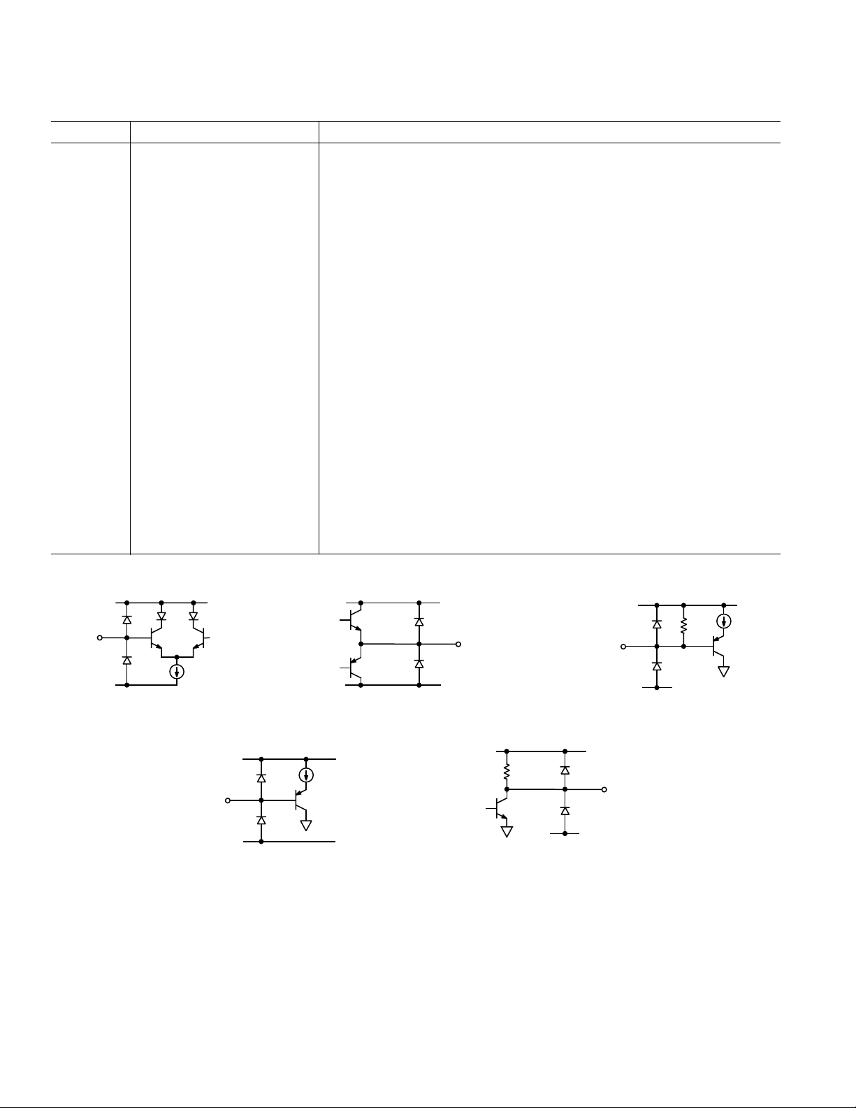
V
ESD
INPUT
ESD
V
a. Analog Input
V
CC
EE
V
CC
ESD
INPUT
ESD
V
EE
d. Logic Input
CC
ESD
ESD
V
EE
b. Analog Output
OUTPUT
V
CC
2k⍀
ESD
ESD
V
EE
e. Logic Output
V
CC
RESET
ESD
c. Reset Input
OUTPUT
ESD
20k⍀
Figure 5. I/O Pin Schematics
–6–
REV. B

AGND
128
1
AGND
2
IN00
3
AGND
4
IN01
5
AGND
6
IN02
7
AGND
8
IN03
9
AGND
10
IN04
11
AGND
12
IN05
13
AGND
14
IN06
15
AGND
16
IN07
17
AGND
18
IN08
19
AGND
20
IN09
21
AGND
22
IN10
23
AGND
24
IN11
25
AGND
26
IN12
27
AGND
28
IN13
29
AGND
30
IN14
31
AGND
32
IN15
33
AGND
NC = NO CONNECT
DVCC
DATA IN
126
127
PIN 1
IDENTIFIER
343536
DVCC
DATA OUT
CLK
DATA OUT
124
125
37
CLK
DATA IN
RESET
UPDATE
122
123
39
38
RESET
UPDATE
CE
121
40
CE
PIN CONFIGURATION
DGND
DVEE
AVEE
AVEE
AVEE
AVCC
AVCC
AVCCNCNCNCNC
117
116
115
114
AD8116
128L LQFP
(14mm x 14mm)
TOP VIEW
(Not to Scale)
47
46
AVEE
AVCC
AVCC
113
4849505152
AVCC
120
119
41
42
DVEE
DGND
118
434445
AVEE
AVEE
111
112
110
NCNCNC
NCNCNCNCAGND00
108
109
107
106
105
53
54
56
55
NCNCNC
NC
AGND15
AGND01
104
103
58
57
AGND14
AGND13
AGND02
AGND03
101
102
59
60
AGND12
AGND11
AGND04
AGND05
999897
100
61
62
AGND10
AGND09
AGND06
AGND07
64
63
AVCC15
AGND08
96
AVCC00
95
OUT00
94
AVEE00/01
93
OUT01
92
AVCC01/02
91
OUT02
90
AVEE02/03
89
OUT03
88
AVCC03/04
87
OUT04
86
AVEE04/05
85
OUT05
AVCC05/06
84
83
OUT06
AVEE06/07
82
OUT07
81
AVCC07/08
80
OUT08
79
AVEE08/09
78
OUT09
77
AVCC09/10
76
OUT10
75
AVEE10/11
74
OUT11
73
AVCC11/12
72
OUT12
71
AVEE12/13
70
OUT13
69
AVCC13/14
68
OUT14
67
AVEE14/15
66
OUT15
65
AD8116
REV. B
–7–
AD8116
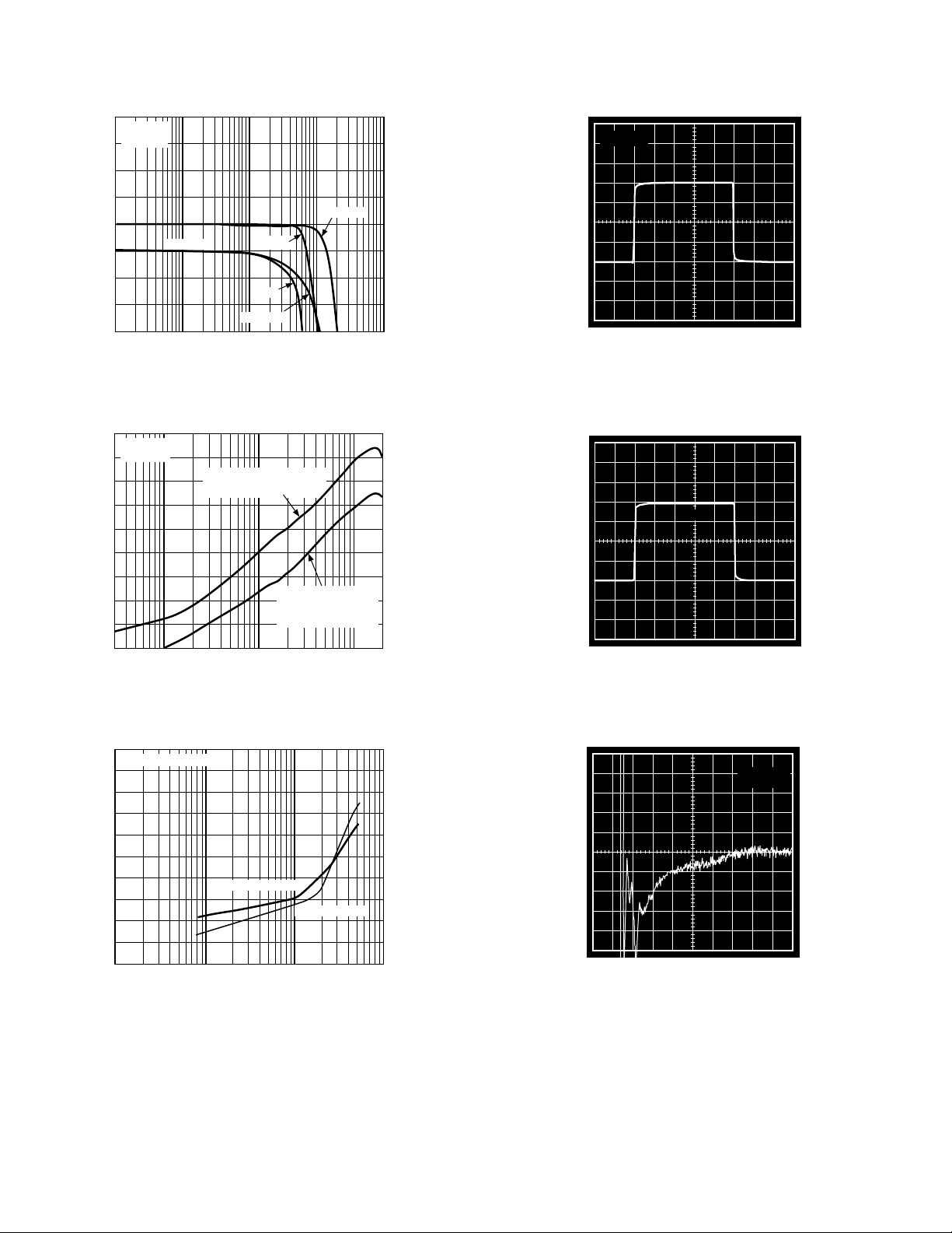
–Typical Performance Characteristics
4
RL = 150⍀
= 0pF
C
3
L
2
1
0
2V p-p
2V p-p
200mV p-p
10M 100M
–1
MAGNITUDE – dB
–2
–3
–4
100k 1G1M
FLATNESS
FREQUENCY – Hz
TPC 1. Frequency Response
–10
RL = 1k⍀
R
= 37.5⍀
–20
S
–30
–40
–50
–60
–70
CROSSTALK – dB
–80
–90
–100
300k 200M1M 10M 100M
ALL HOSTILE CROSSTALK
V
= 632mV p-p
IN
FREQUENCY – Hz
200mV p-p
ADJACENT CHANNEL
CROSSTALK
V
= 632mV p-p
IN
0.5
0.4
0.3
0.2
0.1
0
–0.1
–0.2
–0.3
100mV p-p
25mV/DIV
FLATNESS – dB
100ns/DIV
TPC 4. Step Response, 100 mV Step
2V p-p
500mV/DIV
100ns/DIV
TPC 2. Crosstalk vs. Frequency
0
VIN = 2V p-p, RL = 150⍀
–10
–20
–30
–40
–50
–60
–70
HARMONIC DISTORTION – dB
–80
–90
–100
100k 1M 10M 100M
2ND HARMONIC
3RD HARMONIC
FREQUENCY – Hz
TPC 3. Total Harmonic Distortion
TPC 5. Step Response, 2 V Step
2mV/DIV
= 0.1%/DIV
0 20 40 60 80 100 120 140 160 180
20ns/DIV
TPC 6. Settling Time
2V STEP
= 150⍀
R
L
–8–
REV. B
–20
Typical Performance Characteristics–
AD8116
–30
–40
–50
–60
POWER SUPPLY REJECTION – dB
–70
10k 10M100k 1M
FREQUENCY – Hz
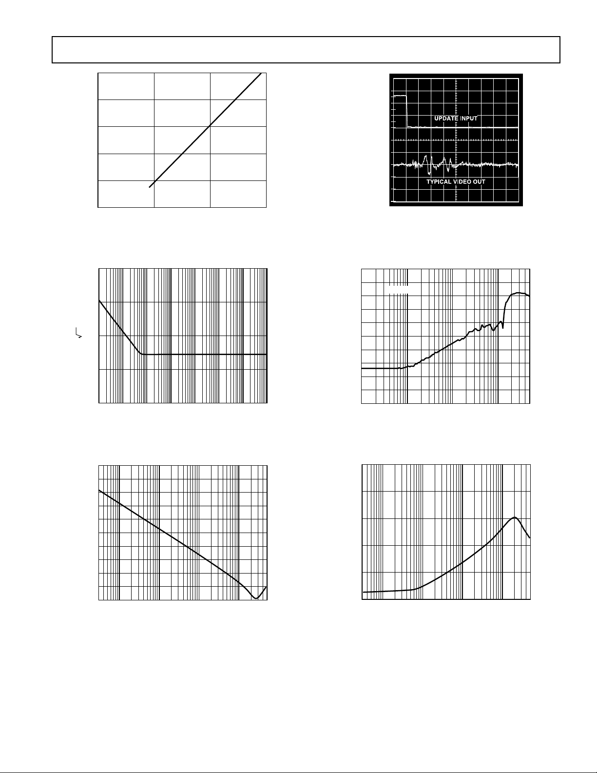
TPC 7. PSRR vs. Frequency
316
100
31.6
nV/ Hz
10
3.16
10 100M100
1k 10k 100k 1M 10M
FREQUENCY – Hz
5
4
3
1V/DIV
2
1
0
20
10
10mV/DIV
0
–10
–20
50ns/DIV
TPC 10. Switching Transient (Glitch)
–50
–60
–70
–80
–90
–100
–110
–120
OFF ISOLATION – dB
–130
–140
–150
100k 500M1M 10M 100M
VIN = 2V p-p
FREQUENCY – Hz
TPC 8. Voltage Noise vs. Frequency
10M
1M
100k
10k
OUTPUT IMPEDANCE – ⍀
1k
100
100k 500M1M 10M 100M
FREQUENCY – Hz
TPC 9. Output Impedance, Disabled
TPC 11. Off Isolation, Input-Output
10,000
1000
100
10
OUTPUT IMPEDANCE – ⍀
1
0.1
100k 500M1M 10M 100M
FREQUENCY – Hz
TPC 12. Output Impedance, Enabled
REV. B
–9–
 Loading...