Analog Devices AD8115, AD8114 Datasheet
Low Cost 225 MHz
a
FEATURES
16 ⴛ 16 High Speed Nonblocking Switch Arrays
AD8114; G = +1
AD8115; G = +2
Serial or Parallel Programming of Switch Array
Serial Data Out Allows “Daisy Chaining” of Multiple
16 ⴛ 16s to Create Larger Switch Arrays
High Impedance Output Disable Allows Connection of
Multiple Devices Without Loading the Output Bus
For Smaller Arrays See Our AD8108/AD8109 (8 ⴛ 8) or
AD8110/AD8111 (16 ⴛ 8) Switch Arrays
Complete Solution
Buffered Inputs
Programmable High Impedance Outputs
16 Output Amplifiers, AD8114 (G = +1), AD8115 (G = +2)
Drives 150 ⍀ Loads
Excellent Video Performance
25 MHz, 0.1 dB Gain Flatness
0.05%/0.05ⴗ Differential Gain/Differential Phase Error
= 150 ⍀)
(R
L
Excellent AC Performance
–3 dB Bandwidth: 225 MHz
Slew Rate: 375 V/s
Low Power of 700 mW (2.75 mW per Point)
Low All Hostile Crosstalk of –70 dB @ 5 MHz
Reset Pin Allows Disabling of All Outputs (Connected
Through a Capacitor to Ground Provides “Power-On”
Reset Capability)
100-Lead LQFP Package (14 mm ⴛ 14 mm)
APPLICATIONS
Routing of High Speed Signals Including:
Video (NTSC, PAL, S, SECAM, YUV, RGB)
Compressed Video (MPEG, Wavelet)
3-Level Digital Video (HDB3)
Datacomms
Telecomms
PRODUCT DESCRIPTION
The AD8114/AD8115 are high speed 16 × 16 video crosspoint
switch matrices. They offer a –3 dB signal bandwidth greater
than 200 MHz and channel switch times of less than 50 ns with
1% settling. With –70 dB of crosstalk and –90 dB isolation (@
5 MHz), the AD8114/AD8115 are useful in many high speed
applications. The differential gain and differential phase of
better than 0.05% and 0.05° respectively, along with 0.1 dB
flatness out to 25 MHz while driving a 75 Ω back-terminated
load, make the AD8114/AD8115 ideal for all types of signal
switching.
*Patent Pending.
16 ⴛ 16 Crosspoint Switches
AD8114/AD8115*
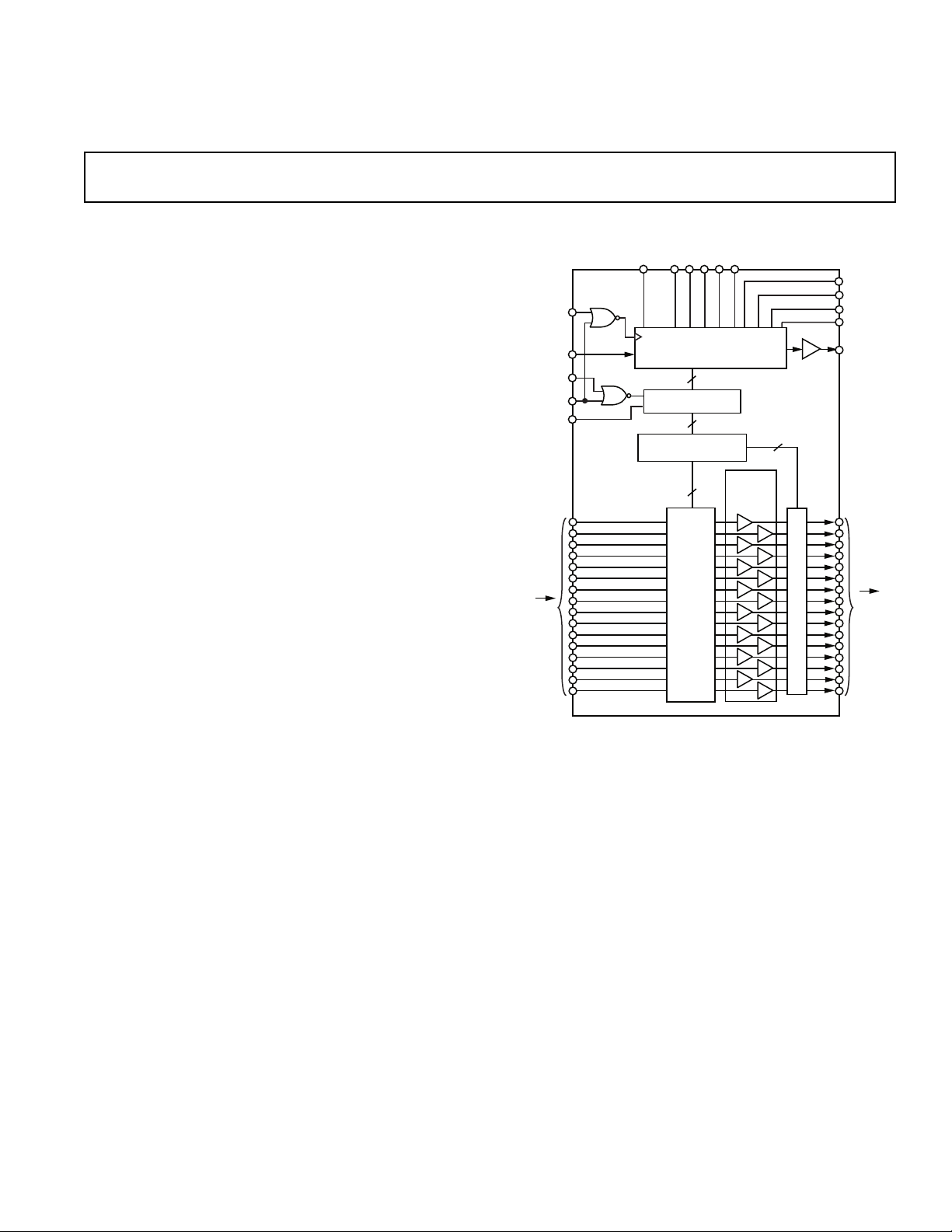
FUNCTIONAL BLOCK DIAGRAM
SER/PAR
CLK
DATA IN
UPDATE
CE
RESET
AD8114/AD8115
16 INPUTS
The AD8114 /AD8115 include 16 independent output buffers
that can be placed into a high impedance state for paralleling
crosspoint outputs so that off channels do not load the output
bus. The AD8114 has a gain of +1, while the AD8115 offers
a gain of +2. They operate on voltage supplies of ±5 V while
consuming only 70 mA of idle current. The channel switching
is performed via a serial digital control (which can accommodate “daisy chaining” of several devices) or via a parallel control
allowing updating of an individual output without reprogramming the entire array.
The AD8114/AD8115 is packaged in 100-lead LQFP package
and is available over the extended industrial temperature range
of –40°C to +85°C.
D0 D1 D2 D3
80-BIT SHIFT REGISTER
PARALLEL LOADING
PARALLEL LATCH
DECODE
16 3 5:16 DECODERS
SWITCH
MATRIX
D4
WITH 5-BIT
80
80
256
OUTPUT
BUFFER
G = +1,
G = +2
16
ENABLE/DISABLE
A0
A1
A2
A3
DATA
OUT
TO "OFF"
SET INDIVIDUAL OR
RESET ALL OUTPUTS
16
OUTPUTS
REV. 0
Information furnished by Analog Devices is believed to be accurate and
reliable. However, no responsibility is assumed by Analog Devices for its
use, nor for any infringements of patents or other rights of third parties
which may result from its use. No license is granted by implication or
otherwise under any patent or patent rights of Analog Devices.
One Technology Way, P.O. Box 9106, Norwood, MA 02062-9106, U.S.A.
Tel: 781/329-4700 World Wide Web Site: http://www.analog.com
Fax: 781/326-8703 © Analog Devices, Inc., 1998

AD8114/AD8115–SPECIFICATIONS
(VS = ⴞ5 V, TA = +25ⴗC, RL = 1 k⍀ unless otherwise noted)
AD8114 /AD8115
Parameter Conditions Min Typ Max Units
DYNAMIC PERFORMANCE
–3 dB Bandwidth 200 mV p-p, R
2 V p-p, R
Gain Flatness 0.1 dB, 200 mV p-p, R
0.1 dB, 2 V p-p, R
Propagation Delay 2 V p-p, R
Settling Time 0.1%, 2 V Step, R
Slew Rate 2 V Step, R
= 150 Ω 150/125 225/200 MHz
L
= 150 Ω 100/125 MHz
L
= 150 Ω 5ns
L
= 150 Ω 375/450 V/µs
L
= 150 Ω 25/40 MHz
L
= 150 Ω 20/40 MHz
L
= 150 Ω 40 ns
L
NOISE/DISTORTION PERFORMANCE
Differential Gain Error NTSC or PAL, R
NTSC or PAL, R
Differential Phase Error NTSC or PAL, R
NTSC or PAL, R
= 1 kΩ 0.05 %
L
= 150 Ω 0.05 %
L
= 1 kΩ 0.05 Degrees
L
= 150 Ω 0.05 Degrees
L
Crosstalk, All Hostile f = 5 MHz –70/–64 dB
f = 10 MHz –60/–52 dB
Off Isolation, Input-Output f = 10 MHz, R
= 150 Ω, One Channel –90 dB
L
Input Voltage Noise 0.01 MHz to 50 MHz 16/18 nV/√Hz
DC PERFORMANCE
Gain Error No Load 0.05/0.2 0.08/0.6 %
R
= 1 kΩ 0.05/0.2 %
L
R
= 150 Ω 0.2/0.35 %
L
Gain Matching No Load, Channel-Channel 0.01/0.5 0.04/1 %
R
= 1 kΩ, Channel-Channel 0.01/0.5 %
L
Gain Temperature Coefficient 0.75/1.5 ppm/°C
OUTPUT CHARACTERISTICS
Output Impedance DC, Enabled 0.2 Ω
Disabled 10 MΩ
Output Disable Capacitance Disabled 5 pF
Output Leakage Current Disabled 1 µA
Output Voltage Range No Load ±3.0 ±3.3 V
Voltage Range I
= 20 mA ±2.5 ±3V
OUT
Short Circuit Current 65 mA
INPUT CHARACTERISTICS
Input Offset Voltage Worst Case (All Configurations) 3 15 mV
Temperature Coefficient 10 µV/°C
Input Voltage Range No Load ±3/±1.5 ±3.5 V
Input Capacitance Any Switch Configuration 5 pF
Input Resistance 110 MΩ
Input Bias Current Per Output Selected 2 5 µA
SWITCHING CHARACTERISTICS
Enable On Time 60 ns
Switching Time, 2 V Step 50% UPDATE to 1% Settling 50 ns
Switching Transient (Glitch) 20/30 mV p-p
POWER SUPPLIES
Supply Current AVCC, Outputs Enabled, No Load 70/80 mA
AVCC, Outputs Disabled 27/30 mA
AVEE, Outputs Enabled, No Load 70/80 mA
AVEE, Outputs Disabled 27/30 mA
DVCC, Outputs Enabled, No Load 16 mA
Supply Voltage Range ±4.5 to ±5.5 V
PSRR DC 64 80 dB
f = 100 kHz 66 dB
f = 1 MHz 46 dB
OPERATING TEMPERATURE RANGE
Temperature Range Operating (Still Air) –40 to +85 °C
θ
JA
Specifications subject to change without notice.
Operating (Still Air) 40 °C/W
–2–
REV. 0
AD8114/AD8115
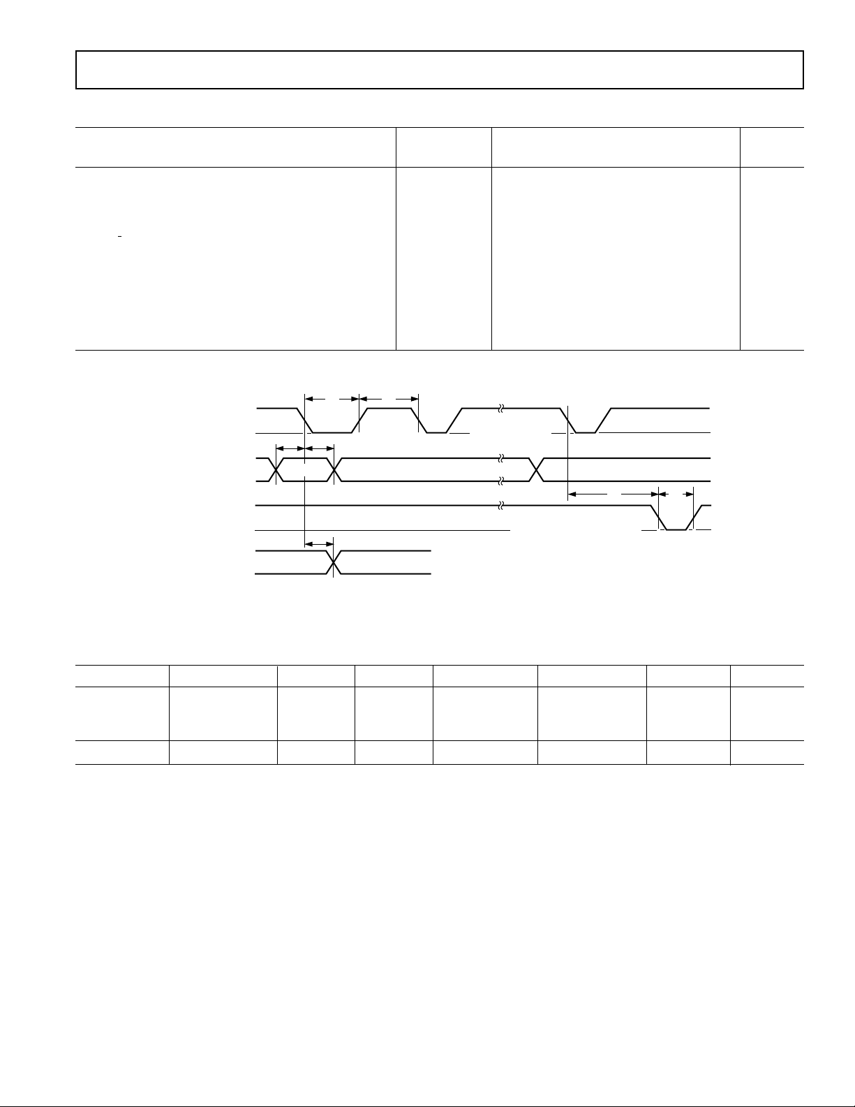
TIMING CHARACTERISTICS (Serial)
␣ Limit
Parameter Symbol Min Typ Max Units
Serial Data Setup Time t
CLK Pulsewidth t
Serial Data Hold Time t
CLK Pulse Separation, Serial Mode t
CLK to UPDATE Delay t
UPDATE Pulsewidth t
CLK to DATA OUT Valid, Serial Mode t
1
2
3
4
5
6
7
20 ns
100 ns
20 ns
100 ns
0ns
50 ns
200 ns
Propagation Delay, UPDATE to Switch On or Off – 50 ns
Data Load Time, CLK = 5 MHz, Serial Mode – 16 µs
CLK, UPDATE Rise and Fall Times – 100 ns
RESET Time – 200 ns
CLK
DATA IN
1 = LATCHED
UPDATE
0 = TRANSPARENT
DATA OUT
t
1
0
t1t
1
OUT7 (D4) OUT7 (D3) OUT00 (D0)
0
2
3
t
7
t
4
LOAD DATA INTO
SERIAL REGISTER
ON FALLING EDGE
t
5
TRANSFER DATA FROM SERIAL
REGISTER TO PARALLEL
LATCHES DURING LOW LEVEL
t
6
Figure 1. Timing Diagram, Serial Mode
Table I. Logic Levels
V
IH
RESET, SER/PAR RESET, SER/PAR RESET, SER/PAR RESET, SER/PAR
CLK, DATA IN, CLK, DATA IN, CLK, DATA IN, CLK, DATA IN,
CE, UPDATE CE, UPDATE DATA OUT DATA OUT CE, UPDATE CE, UPDATE DATA OUT DATA OUT
2.0 V min 0.8 V max 2.7 V min 0.5 V max 20 µA max –400 µA min –400 µA max 3.0 mA min
V
IL
V
OH
V
OL
I
IH
I
IL
I
OH
I
OL
–3–REV. 0
AD8114/AD8115
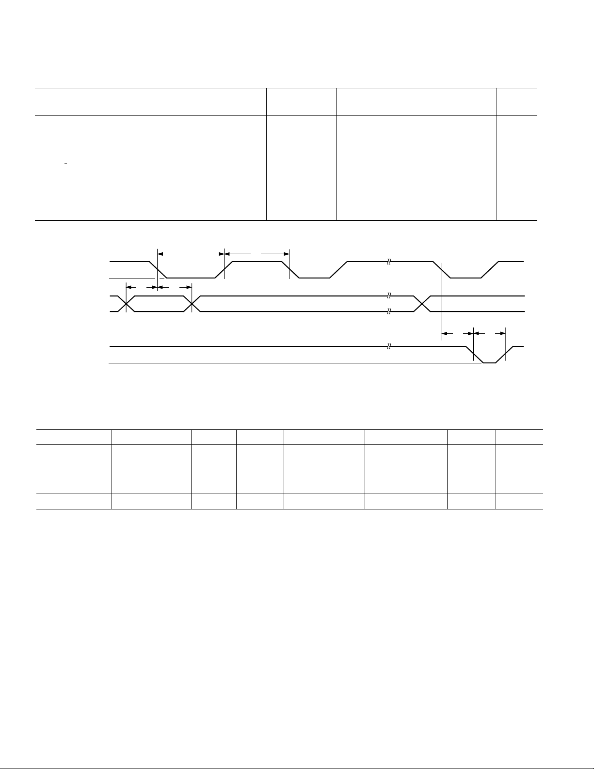
TIMING CHARACTERISTICS (Parallel)
␣ Limit
Parameter Symbol Min Max Units
Data Setup Time t
CLK Pulsewidth t
Data Hold Time t
CLK Pulse Separation t
CLK to UPDATE Delay t
UPDATE Pulsewidth t
1
2
3
4
5
6
20 ns
100 ns
20 ns
100 ns
0ns
50 ns
Propagation Delay, UPDATE to Switch On or Off – 50 ns
CLK, UPDATE Rise and Fall Times – 100 ns
RESET Time – 200 ns
t
4
t
5
t
6
CLK
D0–D4
A0–A2
1 = LATCHED
UPDATE
0 = TRANSPARENT
t
1
0
1
0
t
1
2
t
3
Figure 2. Timing Diagram, Parallel Mode
Table II.␣ Logic Levels
V
IH
RESET, SER/PAR RESET, SER/PAR RESET, SER/PAR RESET, SER/PAR
CLK, D0, D1, D2, D3, CLK, D0, D1, D2, D3, CLK, D0, D1, D2, D3, CLK, D0, D1, D2, D3,
D4, A0, A1, A2, A3 D4, A0, A1, A2, A3 D4, A0, A1, A2, A3 D4, A0, A1, A2, A3
CE, UPDATE CE, UPDATE DATA OUT DATA OUT CE, UPDATE CE, UPDATE DATA OUT DATA OUT
2.0 V min 0.8 V max 2.7 V min 0.5 V max 20 µA max –400 µA min –400 µA max 3.0 mA min
V
IL
V
OH
V
OL
I
IH
I
IL
I
OH
I
OL
–4–
REV. 0
AD8114/AD8115
WARNING!
ESD SENSITIVE DEVICE
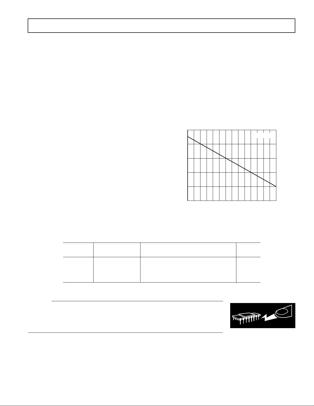
AMBIENT TEMPERATURE – 8C
5.0
MAXIMUM POWER DISSIPATION – Watts
4.0
0
–50 80–40 –30 –20 –10 0 10 20 30 40 50 60 70
3.0
2.0
1.0
TJ = +1508C
90
ABSOLUTE MAXIMUM RATINGS
Supply Voltage . . . . . . . . . . . . . . . . . . . . . . . . . . . . . . . .12.0 V
Internal Power Dissipation
2
1
AD8114/AD8115 100-Lead Plastic LQFP (ST) . . . . 2.6 W
Input Voltage . . . . . . . . . . . . . . . . . . . . . . . . . . . . . . . . . . .±V
S
Output Short Circuit Duration
. . . . . . . . . . . . . . . . . . . . . . Observe Power Derating Curves
Storage Temperature Range . . . . . . . . . . . . –65°C to +125°C
Lead Temperature Range (Soldering 10 sec) . . . . . . . .+300°C
NOTES
1
Stresses above those listed under Absolute Maximum Ratings may cause perma-
nent damage to the device. This is a stress rating only; functional operation of the
device at these or any other conditions above those indicated in the operational
section of this specification is not implied. Exposure to absolute maximum rating
conditions for extended periods may affect device reliability.
2
Specification is for device in free air (T
100-lead plastic LQFP (ST): θJA = 40°C/W.
= +25°C):
A
MAXIMUM POWER DISSIPATION
The maximum power that can be safely dissipated by the
AD8114/AD8115 is limited by the associated rise in junction
temperature. The maximum safe junction temperature for plastic encapsulated devices is determined by the glass transition
temperature of the plastic, approximately +150°C. Temporarily
exceeding this limit may cause a shift in parametric performance
due to a change in the stresses exerted on the die by the pack-
age. Exceeding a junction temperature of +175°C for an ex-
tended period can result in device failure.
While the AD8114/AD8115 is internally short circuit protected,
this may not be sufficient to guarantee that the maximum junc-
tion temperature (+150°C) is not exceeded under all conditions.
To ensure proper operation, it is necessary to observe the maximum power derating curves shown in Figure 3.
Figure 3. Maximum Power Dissipation vs. Temperature
ORDERING GUIDE
Temperature Package Package
Model Range Description Option
AD8114AST –40°C to +85°C 100-Lead Plastic LQFP (14 mm × 14 mm) ST-100
AD8115AST –40°C to +85°C 100-Lead Plastic LQFP (14 mm × 14 mm) ST-100
AD8114-EB Evaluation Board
AD8115-EB Evaluation Board
CAUTION
ESD (electrostatic discharge) sensitive device. Electrostatic charges as high as 4000 V readily
accumulate on the human body and test equipment and can discharge without detection.
Although the AD8114/AD8115 features proprietary ESD protection circuitry, permanent damage may occur on devices subjected to high energy electrostatic discharges. Therefore, proper
ESD precautions are recommended to avoid performance degradation or loss of functionality.
–5–REV. 0
AD8114/AD8115
Table III. Operation Truth Table
SER/
CE UPDATE CLK DATA IN DATA OUT RESET PAR Operation/Comment
1 X X X X X X No change in logic.
01 f Data
i
01 f D0 . . . D4, NA in Parallel 1 1 The data on the parallel data lines, D0–D4, are
A0...A3 Mode loaded into the 80-bit serial shift register loca-
0 0 X X X 1 X Data in the 80-bit shift register transfers into the
X X X X X 0 X Asynchronous operation. All outputs are disabled.
Data
i-80
1 0 The data on the serial DATA IN line is loaded
into serial register. The first bit clocked into
the serial register appears at DATA OUT 80
clocks later.
tion addressed by A0–A3.
parallel latches that control the switch array.
Latches are transparent.
Remainder of logic is unchanged.
PARALLEL
DATA
(OUTPUT
ENABLE)
SER/PAR
DATA IN
(SERIAL)
CLK
CE
UPDATE
OUTPUT
ADDRESS
A0
A1
A2
A3
4 TO 16 DECODER
D0
D1
D2
D3
D4
OUT0 EN
OUT1 EN
OUT2 EN
OUT3 EN
OUT4 EN
OUT5 EN
OUT6 EN
OUT7 EN
OUT8 EN
OUT9 EN
OUT10 EN
OUT11 EN
OUT12 EN
OUT13 EN
OUT14 EN
OUT15 EN
D
CLK
S
D1
Q
Q
D0
S
D1
Q
D0
DQ
CLK
S
D1
Q
D0
DQ
CLK
S
D1
Q
D0
DQ
CLK
S
D1
Q
D0
DQ
CLK
S
D1
DQ
Q
D0
CLK
S
D1
Q
D0
DQ
CLK
S
D1
Q
D0
DQ
CLK
S
D1
Q
D0
DQ
CLK
S
D1
Q
D0
DQ
CLK
S
D1
Q
D0
DQ
CLK
S
D1
D0
DATA
Q
D
Q
OUT
CLK
(OUTPUT ENABLE)
RESET
OUT0
B0
DLE
Q
OUT0
B1
DLE
Q
OUT0
B2
DLE
Q
OUT0
B3
DLE
Q
OUT0
EN
DLE
QCLR
OUT1
B0
DLE
Q
OUT14
EN
DLE
QCLR
OUT15
B0
DLE
Q
OUT15
B1
DLE
Q
OUT15
B2
DLE
Q
OUT15
B3
DLE
Q
OUT15
EN
DLE
QCLR
DECODE
256
16
OUTPUT ENABLESWITCH MATRIX
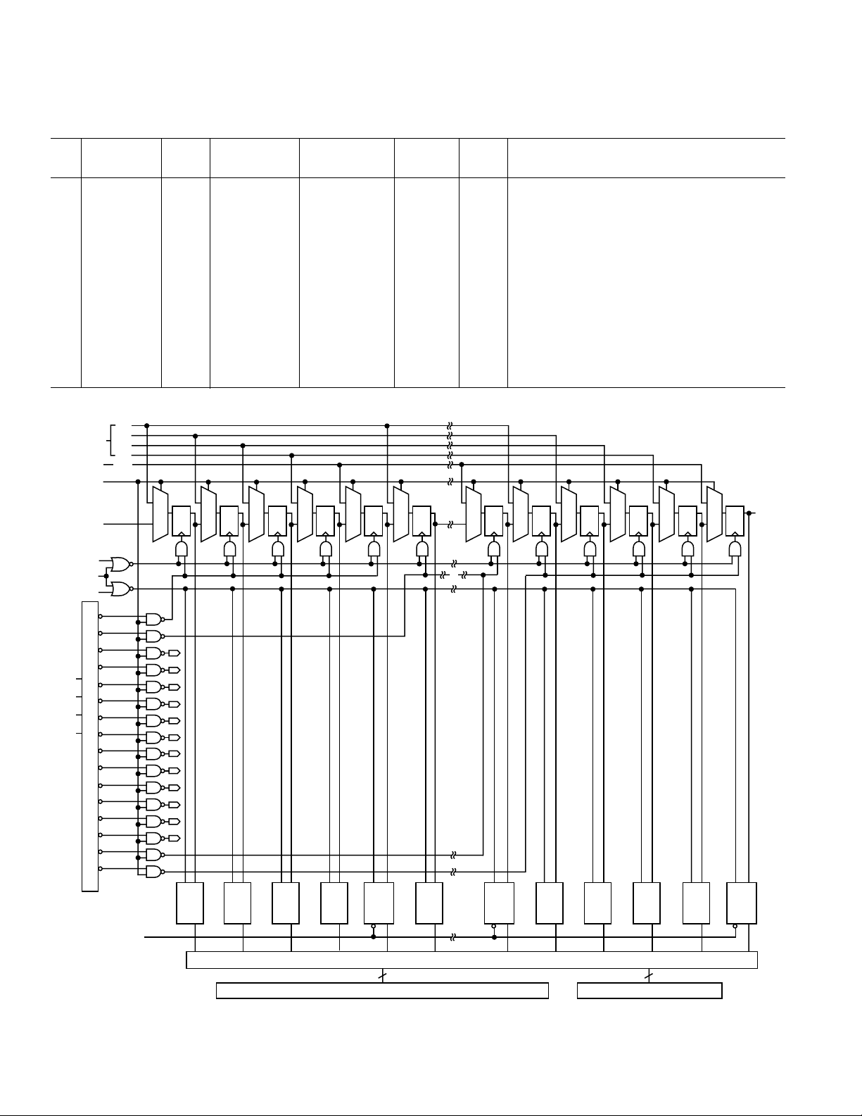
Figure 4. Logic Diagram
–6–
REV. 0
AD8114/AD8115
PIN FUNCTION DESCRIPTIONS
Pin Name Pin Numbers Pin Description
INxx 58, 60, 62, 64, 66, 68, 70, 72, Analog Inputs; xx = Channel Numbers 00 Through 15.
4, 6, 8, 10, 12, 14, 16, 18
DATA IN 96 Serial Data Input, TTL Compatible.
CLK 97 Clock, TTL Compatible. Falling Edge Triggered.
DATA OUT 98 Serial Data Out, TTL Compatible.
UPDATE 95 Enable (Transparent) “Low.” Allows serial register to connect directly to switch matrix.
Data latched when “High.”
RESET 100 Disable Outputs, Active “Low.”
CE 99 Chip Enable, Enable “Low.” Must be “low” to clock in and latch data.
SER/PAR 94 Selects Serial Data Mode, “Low” or Parallel Data Mode, “High.” Must be connected.
OUTyy 53, 51, 49, 47, 45, 43, 41, 39, Analog Outputs yy = Channel Numbers 00 Through 15.
37, 35, 33, 31, 29, 27, 25, 23
AGND 3, 5, 7, 9, 11, 13, 15, 17, 19, 57, Analog Ground for Inputs and Switch Matrix. Must be connected.
59, 61, 63, 65, 67, 69, 71, 73
DVCC 1, 75 +5 V for Digital Circuitry.
DGND 2, 74 Ground for Digital Circuitry.
AVEE 20, 56 –5 V for Inputs and Switch Matrix.
AVCC 21, 55 +5 V for Inputs and Switch Matrix.
AVCCxx/yy 54, 50, 46, 42, 38, 34, 30, 26, 22 +5 V for Output Amplifier that is shared by Channel Numbers xx and yy. Must be connected.
AVEExx/yy 52, 48, 44, 40, 36, 32, 28, 24 –5 V for Output Amplifier that is shared by Channel Numbers xx and yy. Must be connected.
A0 84 Parallel Data Input, TTL Compatible (Output Select LSB).
A1 83 Parallel Data Input, TTL Compatible (Output Select).
A2 82 Parallel Data Input, TTL Compatible (Output Select).
A3 81 Parallel Data Input, TTL Compatible (Output Select MSB).
D0 80 Parallel Data Input, TTL Compatible (Input Select LSB).
D1 79 Parallel Data Input, TTL Compatible (Input Select).
D2 78 Parallel Data Input, TTL Compatible (Input Select).
D3 77 Parallel Data Input, TTL Compatible (Input Select MSB).
D4 76 Parallel Data Input, TTL Compatible (Output Enable).
NC 85–93 No Connect.
V
CC
ESD
INPUT
ESD
AV
EE
a. Analog Input c. Reset Input
V
CC
ESD
INPUT
ESD
DGND
V
CC
ESD
ESD
AV
EE
b. Analog Output
OUTPUT
2kV
V
CC
ESD
RESET
ESD
V
CC
ESD
OUTPUT
ESD
DGND
d. Logic Input e. Logic Output
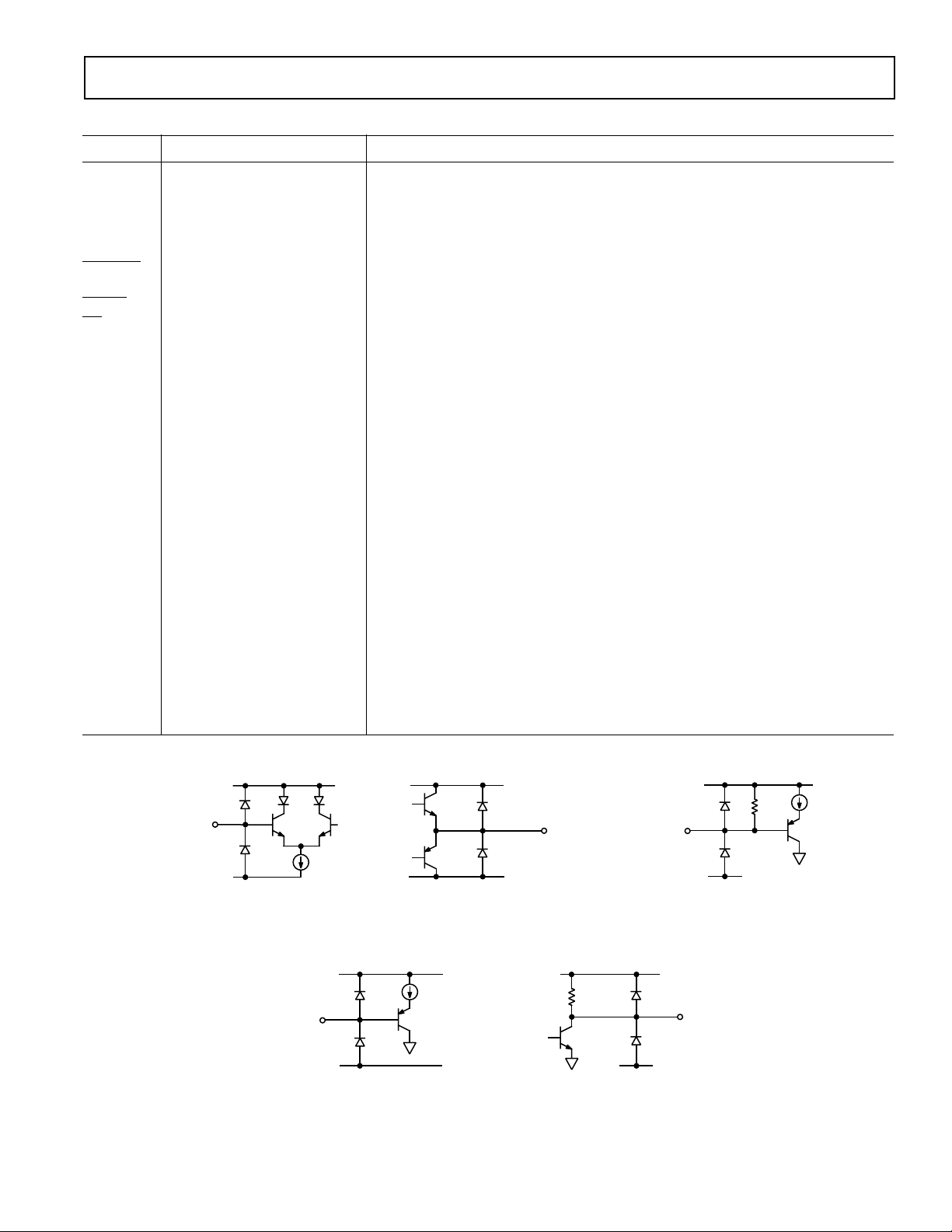
Figure 5. I/O Schematics
–7–REV. 0
20kV
DGND

AD8114/AD8115
PIN CONFIGURATION
DVCC
DGND
AGND
IN08
AGND
IN09
AGND
IN10
AGND
IN11
AGND
IN12
AGND
IN13
AGND
IN14
AGND
IN15
AGND
AVEE
AVCC
AVCC15
OUT15
AVEE14/15
OUT14
CE
RESET
100
1
PIN 1
2
IDENTIFIER
3
4
5
6
7
8
9
10
11
12
13
14
15
16
17
18
19
20
21
22
23
24
25
26
DATA IN
CLK
DATA OUT
9998979695
28
27
29
30
NC
NC
SER/PAR
UPDATE
9493929190
AD8114/AD8115
33
31
32
34
NC
NC
NC
8988878685
TOP VIEW
(Not to Scale)
35
36
37
NC
NC
NC
NC
8483828180
39
40
41
38
42
A3
A2
A1
A0
D0
43
44
45
46
D2
D1
797877
48
47
D4
D3
76
75
DVCC
74
DGND
73
AGND
72
IN07
71
AGND
70
IN06
69
AGND
68
IN05
67
AGND
66
IN04
65
AGND
64
IN03
63
AGND
62
IN02
61
AGND
60
IN01
59
AGND
58
IN00
57
AGND
56
AVEE
55
AVCC
54
AVCC00
53
OUT00
52
AVEE00/01
51
OUT01
50
49
OUT13
OUT12
AVEE12/13
AVCC13/14
NC = NO CONNECT
OUT11
AVEE10/11
AVCC11/12
OUT10
AVCC09/10
OUT09
AVEE08/09
OUT08
AVCC07/08
OUT07
AVEE06/07
OUT06
AVCC05/06
OUT05
AVEE04/05
OUT04
AVCC03/04
OUT03
AVEE02/03
OUT02
AVCC01/02
–8–
REV. 0
 Loading...