ANALOG DEVICES AD8113 Service Manual
Audio/Video 60 MHz
www.BDTIC.com/ADI
a
FEATURES
16 ⴛ 16 High Speed Nonblocking Switch Array
Serial or Parallel Programming of Switch Array
Serial Data Out Allows Daisy Chaining Control of
Multiple 16 ⴛ 16s to Create Larger Switch Arrays
Output Disable Allows Connection of Multiple Devices
without Loading the Output Bus
Complete Solution
Buffered Inputs
16 Output Amplifiers
Operates on ⴞ5 V or ⴞ12 V Supplies
Low Supply Current of 54 mA
=
Excellent Audio Performance V
ⴞ10 V Output Swing
0.002% THD @ 20 kHz Max. 20 V p-p (R
Excellent Video Performance V
10 MHz 0.1 dB Gain Flatness
0.1% Differential Gain Error (R
0.1ⴗ Differential Phase Error (R
Excellent AC Performance
–3 dB Bandwidth 60 MHz
Low All Hostile Crosstalk of
–83
dB @ 20 kHz
Reset Pin Allows Disabling of All Outputs (Connected
to a Capacitor to Ground Provides Power-On
Reset Capability)
100-Lead LQFP (14 mm ⴛ 14 mm)
APPLICATIONS
Analog/Digital Audio Routers
Video Routers (NTSC, PAL, S-VIDEO, SECAM)
Multimedia Systems
Video Conferencing
CCTV Surveillance
S
S
=
= 1 k
L
L
ⴞ12 V
ⴞ5 V
⍀)
= 1 k⍀)
= 600
L
⍀)
16 ⴛ 16, G = ⴙ2 Crosspoint Switch
AD8113
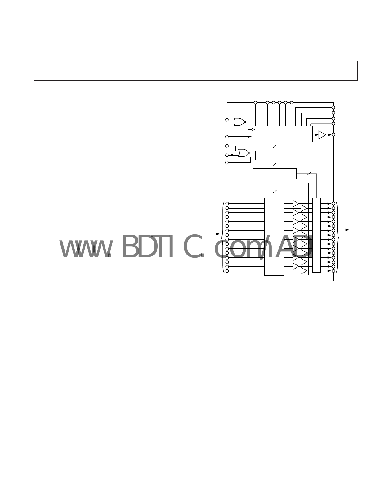
FUNCTIONAL BLOCK DIAGRAM
DATA IN
UPDATE
RESET
16 INPUTS
CLK
CE
SER/PAR
16 ⴛ 5:16 DECODERS
AD8113
D0 D1 D2 D3
80-BIT SHIFT REGISTER
PARALLEL LOADING
PARALLEL LATCH
DECODE
SWITCH
MATRIX
WITH 5-BIT
80
80
256
D4
OUTPUT
BUFFER
G = +2
16
ENABLE/DISABLE
A0
A1
A2
A3
DATA
OUT
TO "OFF"
SET INDIVIDUAL OR
RESET ALL OUTPUTS
16
OUTPUTS
PRODUCT DESCRIPTION
The AD8113 is a fully buffered crosspoint switch matrix that
operates on ±12 V for audio applications and ±5 V for video
applications. It offers a –3 dB signal bandwidth greater than
60 MHz and channel switch times of less than 60 ns with 0.1%
settling for use in both analog and digital audio. The AD8113
operated at 20 kHz has crosstalk performance of –83 dB and
isolation of 90 dB. In addition, ground/power pins surround all
inputs and outputs to provide extra shielding for operation in
the most demanding audio routing applications. The differential
gain and differential phase of better than 0.1% and 0.1°, respectively, along with 0.1 dB flatness out to 10 MHz, make the
AD8113 suitable for many video applications.
The AD8113 includes 16 independent output buffers that can
be placed into a disabled state for paralleling crosspoint outputs
so that off channel loading is minimized. The AD8113 has a
gain of +2. It operates on voltage supplies of ±5 V or ±12 V
while consuming only 34 mA or 31 mA of current, respectively.
The channel switching is performed via a serial digital control
(which can accommodate daisy-chaining of several devices) or
via a parallel control, allowing updating of an individual output
without reprogramming the entire array.
The AD8113 is packaged in a 100-lead LQFP and is available
over the commercial temperature range of 0°C to 70°C.
REV. A
Information furnished by Analog Devices is believed to be accurate and
reliable. However, no responsibility is assumed by Analog Devices for its
use, nor for any infringements of patents or other rights of third parties that
may result from its use. No license is granted by implication or otherwise
under any patent or patent rights of Analog Devices. Trademarks and
registered trademarks are the property of their respective companies.
One Technology Way, P.O. Box 9106, Norwood, MA 02062-9106, U.S.A.
Tel: 781/329-4700 www.analog.com
Fax: 781/326-8703 © 2003 Analog Devices, Inc. All rights reserved.

AD8113–SPECIFICATIONS
www.BDTIC.com/ADI
Parameter Conditions Min Typ Max Unit
DYNAMIC PERFORMANCE
–3 dB Bandwidth V
V
V
V
Gain Flatness 0.1 dB, V
Propagation Delay V
Settling Time 0.1%, 2 V Step, R
Slew Rate 2 V Step, R
20 V Step, RL =600 Ω, VS = ±12 V 120 V/µs
NOISE/DISTORTION PERFORMANCE
Differential Gain Error NTSC, RL = 1 kΩ, VS = ±5 V 0.1 %
Differential Phase Error NTSC, RL = 1 kΩ, VS = ±5 V 0.1 Degrees
Total Harmonic Distortion 20 kHz, RL = 600 Ω, 20 V p-p 0.002 %
Crosstalk, All Hostile f = 5 MHz, R
f = 20 kHz –83 dB
Off Isolation f = 5 MHz, R
f = 20 kHz, One Channel –83 dB
Input Voltage Noise 20 kHz 14 nV/√Hz
0.1 MHz–10 MHz 12 nV/√Hz
DC PERFORMANCE
Gain Error No Load, VS = ±12 V, V
RL = 600 Ω, VS = ±12 V 0.5 %
RL = 150 Ω, VS = ±5 V 0.5 %
Gain Matching No Load, Channel-to-Channel 0.7 3.5 %
RL = 600 Ω, Channel-to-Channel 0.7 %
RL = 150 Ω, Channel-to-Channel 0.7 %
Gain Temperature Coefficient 20 ppm/°C
OUTPUT CHARACTERISTICS
Output Resistance Enabled 0.3 Ω
Disabled 3.4 4 kΩ
Output Capacitance Disabled 5 pF
Output Voltage Swing VS = ±5 V, No Load ±3.2 ±3.5 V
VS = ±12 V, No Load ± 10.3 ±10.5 V
I
OUT
I
Short Circuit Current RL = 0 Ω 55 mA
INPUT CHARACTERISTICS
Input Offset Voltage All Configurations ± 4.5 ±8.5 mV
Input Voltage Range No Load, VS = ±5 V ±1.5 V
Input Capacitance Any Switch Configuration 4 pF
Input Resistance 50 MΩ
Input Bias Current Any Number of Enabled Inputs 1 ±1.6 µA
SWITCHING CHARACTERISTICS
Enable On Time 80 ns
Switching Time, 2 V Step 50% Update to 1% Settling 50 ns
Switching Transient (Glitch) 20 mV p-p
POWER SUPPLIES
Supply Current AVCC Outputs Enabled, No Load, VS = ±12 V 50 54mA
OUT
Temperature Coefficient 10 µV/°C
VS = ±12 V ±5.0 V
AVCC Outputs Disabled, VS = ±12 V 34 38mA
AVCC Outputs Enabled, No Load, VS = ±5 V 45 50mA
AVCC Outputs Disabled, VS = ±5 V 31 35mA
AVEE Outputs Enabled, No Load, VS = ± 12 V 50 54mA
AVEE Outputs Disabled, VS = ±12 V 34 38mA
AVEE Outputs Enabled, No Load, VS = ±5 V 45 50mA
AVEE Outputs Disabled, VS = ±5 V 31 35mA
DVCC Outputs Enabled, No Load 8 13 mA
(TA = 25ⴗC, VS = ⴞ12 V, RL = 600 ⍀, unless otherwise noted.)
= 200 mV p-p, RL = 600 Ω, VS = ±12 V 46 60 MHz
OUT
= 200 mV p-p, RL = 150 Ω, VS = ±5 V 41 60 MHz
OUT
= 8 V p-p, RL = 600 Ω, VS = ±12 V 10 MHz
OUT
= 2 V p-p, RL = 150 Ω, VS = ±5 V 25 MHz
OUT
OUT
= 20 mA, VS = ±5 V ± 2.7 ± 3V
= 20 mA, VS = ±12 V ±9.8 ±10 V
= 200 mV p-p, RL =150 Ω, VS = ±5 V 10 MHz
OUT
= 2 V p-p, RL = 150 Ω 20 ns
=150 Ω, VS = ±5 V 23 ns
L
=150 Ω, VS = ±5 V 100 V/µs
L
=150 Ω, VS = ±5 V –67 dB
L
=150 Ω, VS = ±5 V, One Channel –100 dB
L
= ±8V 0.3 2.5 %
OUT
–2–
REV. A
AD8113
www.BDTIC.com/ADI
Parameter Conditions Min Typ Max Unit
DYNAMIC PERFORMANCE
Supply Voltage Range AV
AV
DV
CC
EE
CC
4.5 12.6 V
–12.6 –4.5 V
4.5 5.5 V
PSRR DC 75 80 dB
f = 100 kHz 60 dB
f = 1 MHz 40 dB
OPERATING TEMPERATURE RANGE
Temperature Range Operating (Still Air) 0 to 70 °C
θ
JA
Specifications subject to change without notice.
Operating (Still Air) 40 °C/W
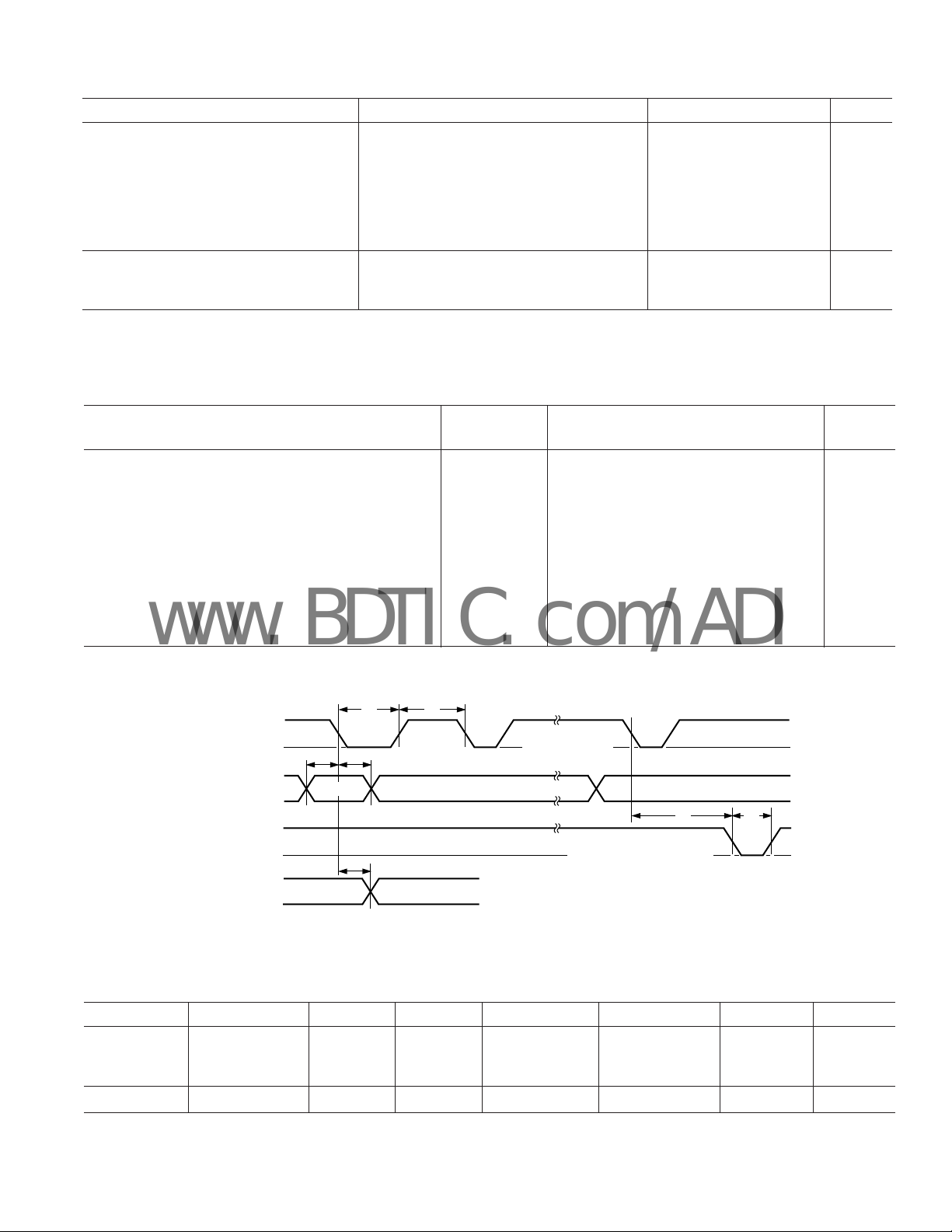
TIMING CHARACTERISTICS (Serial)
Limit
Parameter Symbol Min Typ Max Unit
Serial Data Setup Time t
CLK Pulsewidth t
Serial Data Hold Time t
CLK Pulse Separation, Serial Mode t
CLK to UPDATE Delay t
UPDATE Pulsewidth t
CLK to DATA OUT Valid, Serial Mode t
1
2
3
4
5
6
7
20 ns
100 ns
20 ns
100 ns
0ns
50 ns
200 ns
Propagation Delay, UPDATE to Switch On or Off 50 ns
Data Load Time, CLK = 5 MHz, Serial Mode 16 µs
CLK, UPDATE Rise and Fall Times 100 ns
RESET Time 200 ns
Specifications subject to change without notice.
CLK
DATA IN
1 = LATCHED
UPDATE
0 = TRANSPARENT
DATA OUT
t
1
0
t1t
1
OUT7 (D4) OUT7 (D3) OUT00 (D0)
0
2
3
t
7
t
4
LOAD DATA INTO
SERIAL REGISTER
ON FALLING EDGE
t
5
TRANSFER DATA FROM SERIAL
REGISTER TO PARALLEL
LATCHES DURING LOW LEVEL
t
6
Figure 1. Timing Diagram, Serial Mode
Table I. Logic Levels
V
IH
RESET, SER/PAR RESET, SER/PAR RESET, SER/PAR RESET, SER/PAR
CLK, DATA IN, CLK, DATA IN, CLK, DATA IN, CLK, DATA IN,
CE, UPDATE CE, UPDATE DATA OUT DATA OUT CE, UPDATE CE, UPDATE DATA OUT DATA OUT
2.0 V min 0.8 V max 2.7 V min 0.5 V max 20 µA max –400 µA min –400 µA max 3.0 mA min
REV. A
V
IL
V
OH
V
OL
I
IH
I
IL
–3–
I
OH
I
OL
AD8113
www.BDTIC.com/ADI
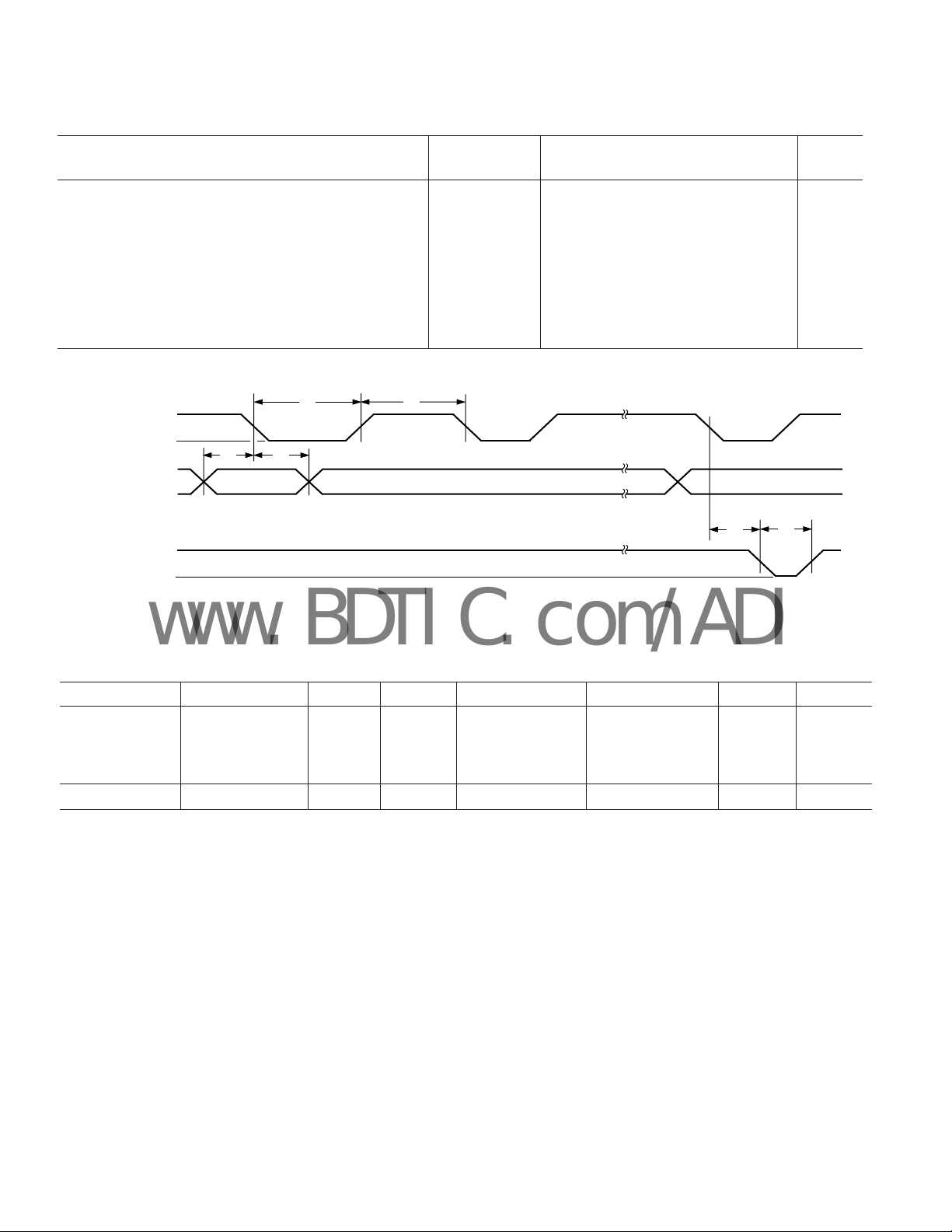
TIMING CHARACTERISTICS (Parallel)
Limit
Parameter Symbol Min Max Unit
Data Setup Time t
CLK Pulsewidth t
Data Hold Time t
CLK Pulse Separation t
CLK to UPDATE Delay t
UPDATE Pulsewidth t
1
2
3
4
5
6
20 ns
100 ns
20 ns
100 ns
0ns
50 ns
Propagation Delay, UPDATE to Switch On or Off 50 ns
CLK, UPDATE Rise and Fall Times 100 ns
RESET Time 200 ns
Specifications subject to change without notice.
t
4
t
t
5
6
CLK
D0–D4
A0–A2
1 = LATCHED
UPDATE
0 = TRANSPARENT
t
1
0
1
0
t
1
2
t
3
Figure 2. Timing Diagram, Parallel Mode
Table II. Logic Levels
V
IH
RESET, SER/PAR RESET, SER/PAR RESET, SER/PAR RESET, SER/PAR
CLK, D0, D1, D2, D3, CLK, D0, D1, D2, D3, CLK, D0, D1, D2, D3, CLK, D0, D1, D2, D3,
D4, A0, A1, A2, A3 D4, A0, A1, A2, A3 D4, A0, A1, A2, A3 D4, A0, A1, A2, A3
CE, UPDATE CE, UPDATE DATA OUT DATA OUT CE, UPDATE CE, UPDATE DATA OUT DATA OUT
2.0 V min 0.8 V max 2.7 V min 0.5 V max 20 µA max –400 µA min –400 µA max 3.0 mA min
V
IL
V
OH
V
OL
I
IH
I
IL
I
OH
I
OL
–4–
REV. A
AD8113
www.BDTIC.com/ADI
ABSOLUTE MAXIMUM RATINGS
Analog Supply Voltage (AV
Digital Supply Voltage (DV
Ground Potential Difference (AGND – DGND) . . . . . ±0.5 V
Internal Power Dissipation
Analog Input Voltage
CC
CC
2
3
. . . . . . . . . . . . . . . . . . . . . 3.1 W
. . . . . . . . . . . Maintain Linear Output
Digital Input Voltage . . . . . . . . . . . . . . . . . . . . . . . . . . DV
1
– AVEE) . . . . . . . . . . . . 26.0 V
– DGND) . . . . . . . . . . . . . . 6 V
CC
Output Voltage (Disabled Output)
. . . . . . . . . . . . . . . . . . . . (AV
– 1.5 V) to (AVEE + 1.5 V)
CC
Output Short-Circuit Duration . . . . . . . . . . . . . . Momentary
Storage Temperature Range . . . . . . . . . . . . –65°C to +125°C
Lead Temperature Range (Soldering 10 sec) . . . . . . . . 300°C
NOTES
1
Stresses above those listed under Absolute Maximum Ratings may cause perma-
nent damage to the device. This is a stress rating only; functional operation of the
device at these or any other conditions above those indicated in the operational
section of this specification is not implied. Exposure to absolute maximum rating
conditions for extended periods may affect device reliability.
2
Specification is for device in free air (TA = 25°C):
100-lead plastic LQFP (ST): θJA = 40°C/W.
3
To avoid differential input breakdown, in no case should one-half the output
voltage (1/2 V
tial. See output voltage swing specification for linear output range.
) and any input voltage be greater than 10 V potential differen-
OUT
POWER DISSIPATION
The AD8113 is operated with ±5 V to ± 12 V supplies and
can drive loads down to 150 Ω (± 5 V) or 600 Ω (±12 V),
resulting in a large range of possible power dissipations. For
this reason, extra care must be taken derating the operating
conditions based on ambient temperature.
Packaged in a 100-lead LQFP, the AD8113 junction-to-ambient
thermal impedance (θ
) is 40°C/W. For long-term reliability,
JA
the maximum allowed junction temperature of the plasticencapsulated die should not exceed 150°C. Temporarily exceeding
this limit may cause a shift in parametric performance due to a
change in the stresses exerted on the die by the package. Exceeding
a junction temperature of 175°C for an extended period can result
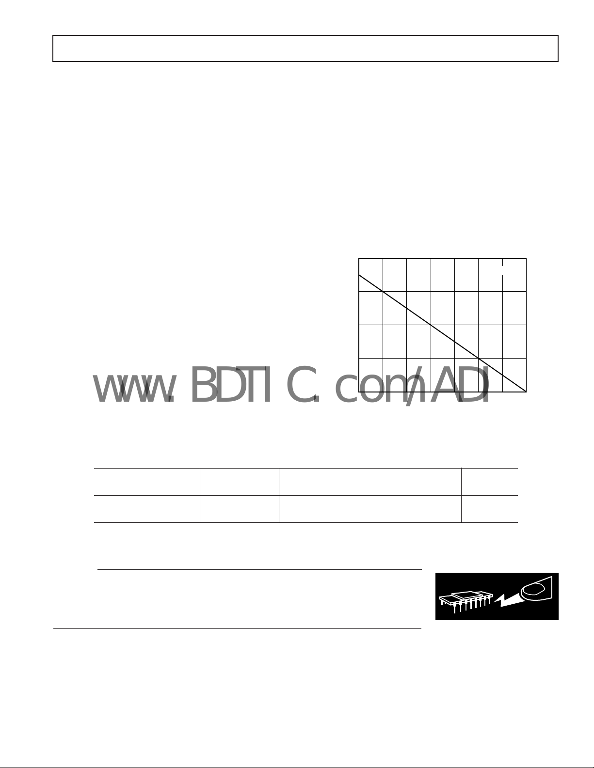
in device failure. The following curve shows the range of allowed
power dissipations that meet these conditions over the commercial
range of ambient temperatures.
4.0
TJ = 150ⴗC
3.5
3.0
2.5
MAXIMUM POWER – Watts
2.0
05010 20 30 40
AMBIENT TEMPERATURE – ⴗC
Figure 3. Maximum Power Dissipation vs. Ambient
Temperature
ORDERING GUIDE
Temperature Package Package
Model Range Description Option
AD8113JST 0°C to 70°C 100-Lead Plastic LQFP (14 mm × 14 mm) ST-100
AD8113-EVAL Evaluation Board
CAUTION
ESD (electrostatic discharge) sensitive device. Electrostatic charges as high as 4000 V readily
accumulate on the human body and test equipment and can discharge without detection.
Although the AD8113 features proprietary ESD protection circuitry, permanent damage may
occur on devices subjected to high energy electrostatic discharges. Therefore, proper ESD
precautions are recommended to avoid performance degradation or loss of functionality.
7060
WARNING!
ESD SENSITIVE DEVICE
REV. A
–5–
AD8113
www.BDTIC.com/ADI
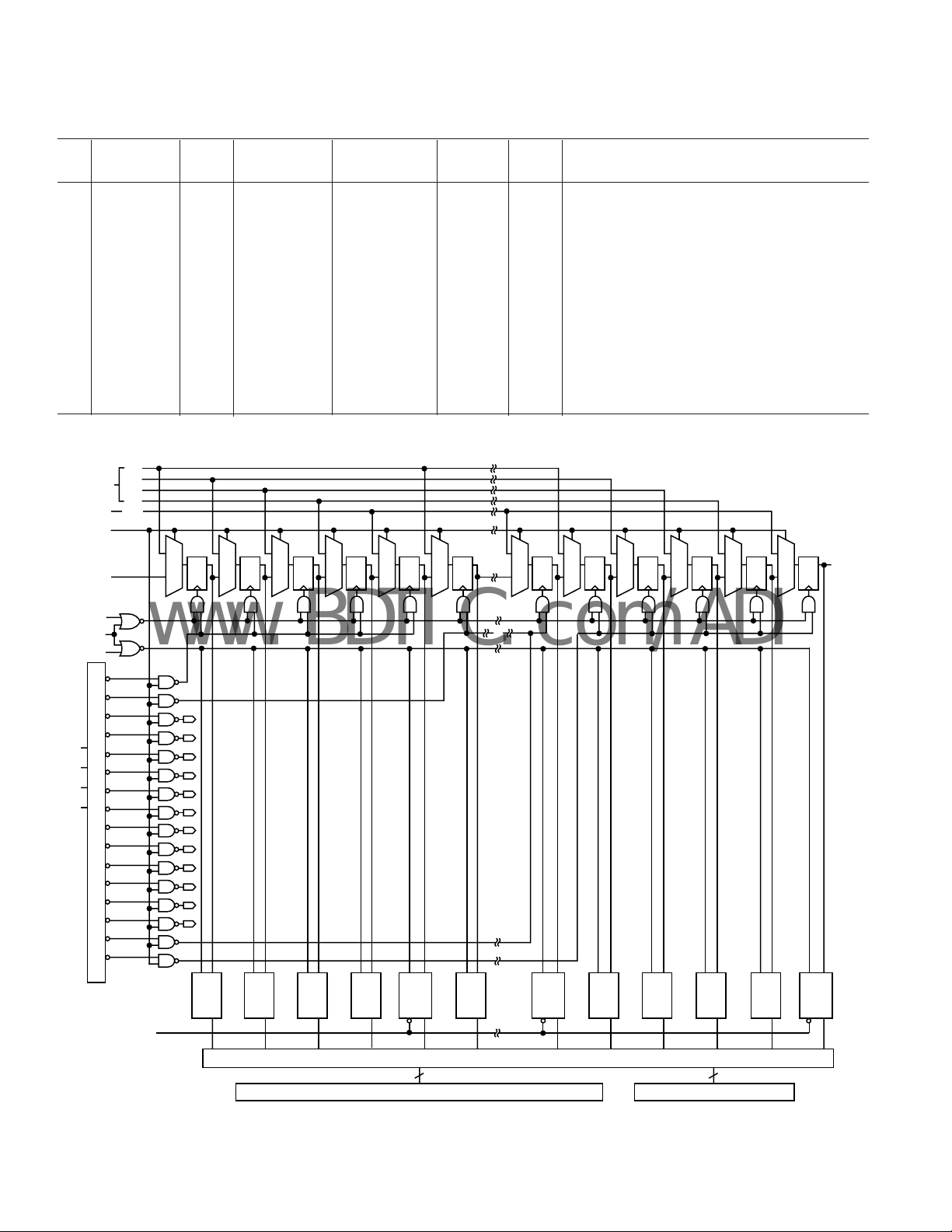
Table III. Operation Truth Table
SER/
CE UPDATE CLK DATA IN DATA OUT RESET PAR Operation/Comment
1X XX XXXNo change in logic.
01 f Data
i
Data
i-80
01 f D0 . ..D4, NA in Parallel 1 1 The data on the parallel data lines, D0–D4, are
A0 ...A3 Mode loaded into the 80-bit serial shift register loca-
00 XX X1XData in the 80-bit shift register transfers into the
XX XX X0XAsynchronous operation. All outputs are disabled.
10The data on the serial DATA IN line is loaded
into serial register. The first bit clocked into
the serial register appears at DATA OUT 80
clocks later.
tion addressed by A0–A3.
parallel latches that control the switch array.
Latches are transparent.
Remainder of logic is unchanged.
PARALLEL
DATA
(OUTPUT
ENABLE)
SER/PAR
DATA IN
(SERIAL)
CLK
CE
UPDATE
OUTPUT
ADDRESS
A0
A1
A2
A3
D0
D1
D2
D3
D4
S
D1
D0
OUT0 EN
OUT1 EN
OUT2 EN
OUT3 EN
OUT4 EN
OUT5 EN
OUT6 EN
OUT7 EN
OUT8 EN
OUT9 EN
OUT10 EN
4 TO 16 DECODER
OUT11 EN
OUT12 EN
OUT13 EN
OUT14 EN
OUT15 EN
S
D1
D
Q
CLK
Q
D0
Q
DQ
CLK
S
D1
Q
D0
DQ
CLK
S
D1
Q
D0
DQ
CLK
S
D1
Q
D0
DQ
CLK
S
D1
DQ
Q
D0
CLK
S
D1
Q
D0
DQ
CLK
S
D1
Q
D0
DQ
CLK
S
D1
Q
D0
DQ
CLK
S
D1
Q
D0
DQ
CLK
S
D1
Q
D0
DQ
CLK
S
D1
D0
DATA
Q
D
Q
OUT
CLK
OUT0
EN
DLE
QCLR
OUT1
B0
DLE
Q
OUT14
EN
DLE
QCLR
OUT15
B0
DLE
OUT15
Q
(OUTPUT ENABLE)
RESET
OUT0
B0
DLE
Q
OUT0
B1
DLE
Q
OUT0
B2
DLE
Q
OUT0
B3
DLE
Q
DECODE
256
Figure 4. Logic Diagram
–6–
DLE
B1
Q
OUT15
B2
DLE
Q
OUT15
B3
DLE
Q
OUT15
EN
DLE
QCLR
16
OUTPUT ENABLESWITCH MATRIX
REV. A
AD8113
ESD
ESD
RESET
V
CC
20k⍀
DGND
ESD
ESD
OUTPUT
V
CC
2k⍀
DGND
www.BDTIC.com/ADI
PIN FUNCTION DESCRIPTIONS
Mnemonic Pin Numbers Pin Description
INxx 58, 60, 62, 64, 66, 68, 70, 72, Analog Inputs; xx = Channel Numbers 00 through 15.
4, 6, 8, 10, 12, 14, 16, 18
DATA IN 96 Serial Data Input, TTL Compatible.
CLK 97 Clock, TTL Compatible. Falling Edge Triggered.
DATA OUT 98 Serial Data Out, TTL Compatible.
UPDATE 95 Enable (Transparent) Low. Allows serial register to connect directly to switch matrix.
Data latched when High.
RESET 100 Disable Outputs, Active Low.
CE 99 Chip Enable, Enable Low. Must be low to clock in and latch data.
SER/PAR 94 Selects Serial Data Mode, Low or Parallel Data Mode, High. Must be connected.
OUTyy 53, 51, 49, 47, 45, 43, 41, 39, Analog Outputs yy = Channel Numbers 00 Through 15.
37, 35, 33, 31, 29, 27, 25, 23
AGND 3, 5, 7, 9, 11, 13, 15, 17, 19, 57, Analog Ground for Inputs and Switch Matrix. Must be connected.
59, 61, 63, 65, 67, 69, 71, 73
DV
CC
DGND 2, 74 Ground for Digital Circuitry.
AV
EE
AV
CC
xx/yy 54, 50, 46, 42, 38, 34, 30, 26, 22 5 V for Output Amplifier that is shared by Channel Numbers xx and yy. Must be connected.
AV
CC
AV
xx/yy 52, 48, 44, 40, 36, 32, 28, 24 –5 V for Output Amplifier that is shared by Channel Numbers xx and yy. Must be connected.
EE
A0 84 Parallel Data Input, TTL Compatible (Output Select LSB).
A1 83 Parallel Data Input, TTL Compatible (Output Select).
A2 82 Parallel Data Input, TTL Compatible (Output Select).
A3 81 Parallel Data Input, TTL Compatible (Output Select MSB).
D0 80 Parallel Data Input, TTL Compatible (Input Select LSB).
D1 79 Parallel Data Input, TTL Compatible (Input Select).
D2 78 Parallel Data Input, TTL Compatible (Input Select).
D3 77 Parallel Data Input, TTL Compatible (Input Select MSB).
D4 76 Parallel Data Input, TTL Compatible (Output Enable).
NC 85–93 No Connect.
1, 75 5 V for Digital Circuitry.
20, 56 –5 V for Inputs and Switch Matrix.
21, 55 5 V for Inputs and Switch Matrix.
V
CC
ESD
INPUT
ESD
AV
EE
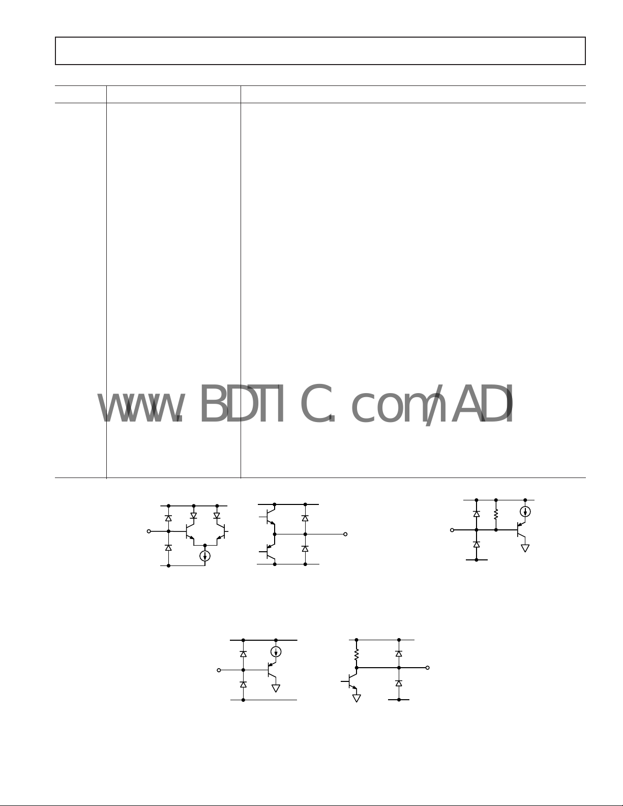
a. Analog Input
V
ESD
INPUT
ESD
DGND
REV. A
d. Logic Input
V
CC
ESD
ESD
AV
EE
b. Analog Output
CC
Figure 5. I/O Schematics
–7–
OUTPUT
e. Logic Output
c. Reset Input

AD8113
www.BDTIC.com/ADI
PIN CONFIGURATION
AV
DV
DGND
AGND
IN08
AGND
IN09
AGND
IN10
AGND
IN11
AGND
IN12
AGND
IN13
AGND
IN14
AGND
IN15
AGND
AV
AV
AVCC15
OUT15
14/15
EE
OUT14
CE
RESET
9998979695
100
1
CC
EE
CC
PIN 1
2
IDENTIFIER
3
4
5
6
7
8
9
10
11
12
13
14
15
16
17
18
19
20
21
22
23
24
25
27
26
DATA IN
CLK
DATA OUT
28
29
30
NC
SER/PAR
UPDATE
9493929190
33
31
32
NC
34
NC
35
NC
NC
NC
8988878685
AD8113
TOP VIEW
(Not to Scale)
38
36
37
NC
39
NC
NC
8483828180
40
41
42
D0
46
D2
D1
797877
48
47
D3
76
75
DV
CC
74
DGND
73
AGND
72
IN07
AGND
71
IN06
70
AGND
69
IN05
68
AGND
67
IN04
66
AGND
65
64
IN03
AGND
63
62
IN02
AGND
61
60
IN01
AGND
59
IN00
58
57
AGND
AV
56
EE
AV
55
CC
54
AVCC00
OUT00
53
52
00/01
AV
EE
OUT01
51
50
49
A3
A2
A1
A0
43
44
45
D4
13/14
12/13
OUT13
OUT12
EE
CC
AV
AV
NC = NO CONNECT
11/12
CC
AV
10/11
OUT11
AV
EE
09/10
OUT10
AV
CC
08/09
OUT09
EE
AV
07/08
OUT08
CC
AV
06/07
OUT07
AV
EE
05/06
OUT06
AV
CC
04/05
OUT05
EE
AV
03/04
OUT04
CC
AV
02/03
OUT03
EE
AV
01/02
OUT02
CC
AV
–8–
REV. A
Typical Performance Characteristics–
www.BDTIC.com/ADI
AD8113
3.0
0.0
GAIN – dB
–3.0
–6.0
0.01 1001010.1
FREQUENCY – MHz
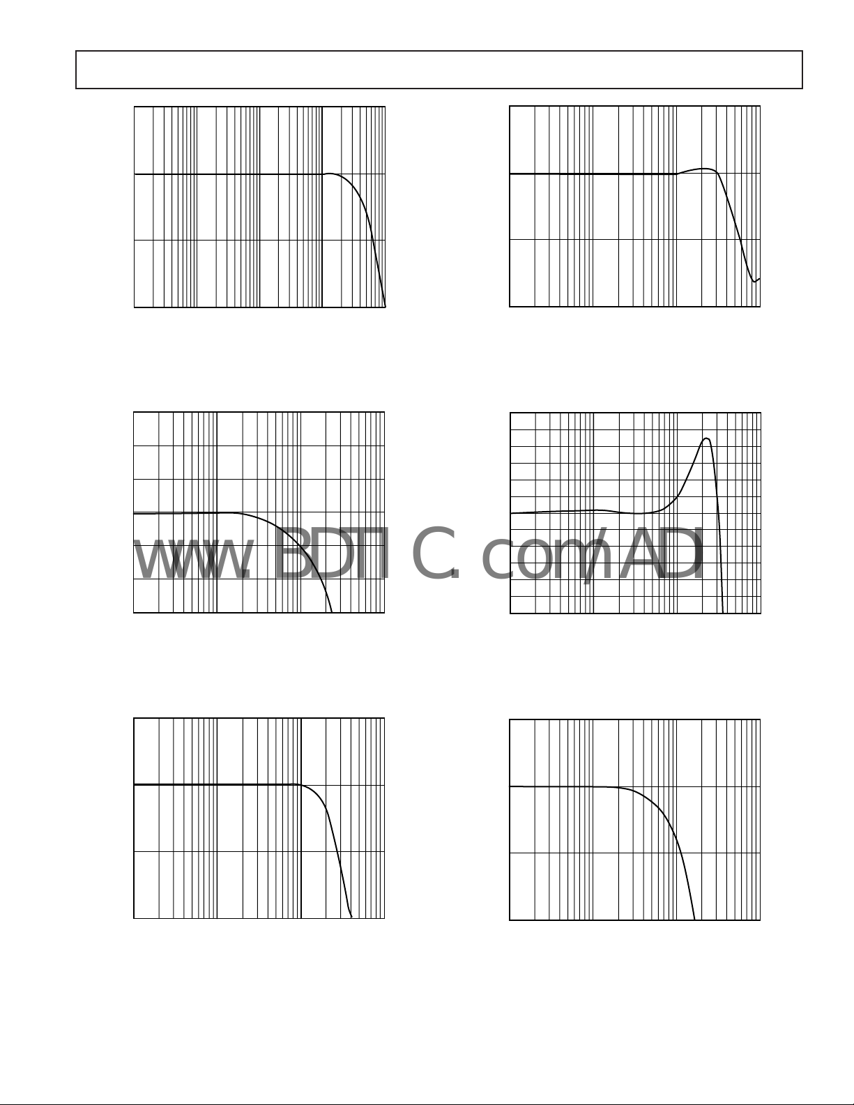
TPC 1. Small Signal Bandwidth, VS = ±5 V, RL = 150Ω,
V
= 200 mV p-p
OUT
0.3
0.2
0.1
3.0
0.0
GAIN – dB
–3.0
–6.0
0.1
FREQUENCY – MHz
100101
TPC 4. Small Signal Bandwidth, VS = ±12 V, RL = 600 Ω,
V
= 200 mV p-p
OUT
0.3
0.2
0.1
0.0
–0.1
GAIN FLATNESS – dB
–0.2
–0.3
0.1
FREQUENCY – MHz
100101
TPC 2. Small Signal Gain Flatness, VS = ±5 V, RL = 150Ω,
V
= 200 mV p-p
OUT
3.0
0.0
GAIN – dB
–3.0
0.0
–0.1
GAIN FLATNESS – dB
–0.2
–0.3
0.1
FREQUENCY – MHz
100101
TPC 5. Small Signal Gain Flatness, VS = ±12 V, RL = 600 Ω,
= 200 mV p-p
V
OUT
3.0
0.0
GAIN – dB
–3.0
–6.0
0.1
FREQUENCY – MHz
100101
TPC 3. Large Signal Bandwidth, VS = ±5 V, RL = 150Ω,
= 2 V p-p
V
OUT
REV. A
–9–
–6.0
0.1
TPC 6. Large Signal Bandwidth, VS = ±12 V, RL = 600 Ω,
V
= 8 V p-p
OUT
FREQUENCY – MHz
100101
 Loading...