Audio/Video, 60 MHz, 16 × 8,
www.BDTIC.com/ADI
FEATURES
Low cost, 16 × 8, high speed, nonblocking switch array
Pin-compatible 16 × 16 version available (AD8113)
Serial or parallel programming of switch array
Serial data out allows daisy chaining control of multiple
16 ×
8 arrays to create larger switch arrays
Output disable allows connection of multiple devices
without loadin
Complete solution
Buffered inputs
8 output amplifiers
Operates on ±5 V or ±12 V supplies
Low supply current of 54 mA
Excellent audio performance V
±10 V output swing
0.002% THD at 20 kHz maximum 20 V p-p (R
Excellent video performance V
0.1 dB gain flatness of 10 MHz
0.1% differential gain error (R
0.1° differential phase error (R
Excellent ac performance
−3 dB bandwidth 60 MHz
Low all-hostile crosstalk of −83 dB at 20 kHz
Reset pin allows disabling of all outputs (connected to a
c
apacitor to ground provides power-on reset capability)
100-lead LQFP (14 mm × 14 mm)
APPLICATIONS
CCTV sur veillance/DVR
Analog/digital audio routers
Video routers (NTSC, PAL, S-Video, SECAM)
Multimedia systems
Video conferencing
g the output bus
= ±12 V
S
= ±5 V
S
L
= 1 kΩ)
= 1 kΩ)
L
= 600 Ω)
L
Gain of +2 Crosspoint Switch
AD8112
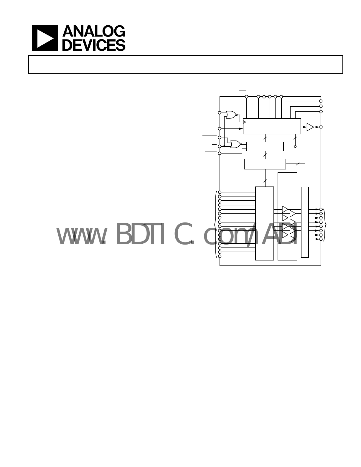
FUNCTIONAL BLOCK DIAGRAM
D0 D1 D2 D3 D4
SER/PAR
A0
A1
CLK
DATA IN
UPDATE
RESET
CE
80-BIT SHIFT REGISTER
WITH 5-BIT
PARALLEL L OADING
40 40
PARALLEL L ATCH
40
DECODE
8 × 5:16 DECODERS
AD8112
16 INPUTS
SWITCH
MATRIX
Figure 1.
128
CONNECT
OUTPUT
BUFFER
G = +2
NO
8
A2
DATA
OUT
TO OFF
SET INDIVIDUAL OR
RESET ALL OUTPUTS
ENABLE/DISABL E
8 OUTPUTS
06523-001
GENERAL DESCRIPTION
The AD8112 is a low cost, fully buffered crosspoint switch matrix
that operates on ±12 V for audio applications and ±5 V for
video applications. It offers a −3 dB signal bandwidth greater
than 60 MHz and channel switch times of less than 60 ns with
0.1% settling for use in both analog and digital audio. The
AD8112 operated at 20 kHz has a crosstalk performance of
−83 dB and isolation of 90 dB. In addition, ground/power pins
surround all inputs and outputs to provide extra shielding for
operation in the most demanding audio routing applications.
With a differential gain and differential phase better than 0.1%
and 0.1°, respectively, and a 0.1 dB flatness output of up to 10 MHz,
The AD8112 includes eight independen
be placed into a disabled state for paralleling crosspoint outputs
so that off channel loading is minimized. The AD8112 has a gain
of +2. It operates on voltage supplies of ±5 V or ±12 V while
consuming only 34 mA or 31 mA of current, respectively. The
channel switching is performed via a serial digital control (which
can accommodate the daisy chaining of several devices) or via
a parallel control, allowing updating of an individual output
without reprogramming the entire array.
The AD8112 is packaged in a 100-lead LQFP and is available
ver the commercial temperature range of 0°C to 70°C.
o
the AD8112 is suitable for many video applications.
Rev. 0
Information furnished by Analog Devices is believed to be accurate and reliable. However, no
responsibility is assumed by Anal og Devices for its use, nor for any infringements of patents or ot her
rights of third parties that may result from its use. Specifications subject to change without notice. No
license is granted by implication or otherwise under any patent or patent rights of Analog Devices.
Trademarks and registered trademarks are the property of their respective owners.
One Technology Way, P.O. Box 9106, Norwood, MA 02062-9106, U.S.A.
Tel: 781.329.4700 www.analog.com
Fax: 781.461.3113 ©2007 Analog Devices, Inc. All rights reserved.
t output buffers that can

AD8112
www.BDTIC.com/ADI
TABLE OF CONTENTS
Features.............................................................................................. 1
Calculation of Power Dissipation............................................. 17
Applications....................................................................................... 1
Functional Block Diagram .............................................................. 1
General Description ......................................................................... 1
Revision History ............................................................................... 2
Specifications..................................................................................... 3
Timing Characteristics (Serial) .................................................. 5
Timing Characteristics (Parallel) ............................................... 6
Absolute Maximum Ratings............................................................ 7
ESD Caution.................................................................................. 7
Power Dissipation......................................................................... 7
Pin Configuration and Function Descriptions............................. 9
I/O Schematics............................................................................ 11
Typical Performance Characteristics ........................................... 12
Theory of Operation ...................................................................... 17
Short-Circuit Output Conditions............................................. 18
Application Notes........................................................................... 19
Serial Programming................................................................... 19
Parallel Programming................................................................ 19
Power-On Reset.......................................................................... 20
Specifying Audio Levels ............................................................ 20
Creating Unity-Gain Channels................................................. 20
Video Signals............................................................................... 20
Creating Larger Crosspoint Arrays.......................................... 21
Multichannel Video and Audio................................................ 23
Crosstalk...................................................................................... 23
PCB Layout...................................................................................... 26
Outline Dimensions....................................................................... 28
Ordering Guide .......................................................................... 28
REVISION HISTORY
2/07—Revision 0: Initial Version
Rev. 0 | Page 2 of 28

AD8112
www.BDTIC.com/ADI
SPECIFICATIONS
TA = 25°C, VS = ±12 V, RL = 600 Ω, unless otherwise noted.
Table 1.
Parameter Conditions Min Typ Max Unit
DYNAMIC PERFORMANCE
−3 dB Bandwidth V
V
V
V
Gain Flatness 0.1 dB, V
Propagation Delay V
Settling Time 0.1%, 2 V Step, RL = 150 Ω, VS = ±5 V 23 ns
Slew Rate 2 V step, RL = 150 Ω, VS = ±5 V 100 V/μs
20 V step, RL = 600 Ω, VS = ±12 V 120 V/μs
NOISE/DISTORTION PERFORMANCE
Differential Gain Error NTSC, RL = 1 kΩ, VS = ±5 V 0.1 %
Differential Phase Error NTSC, RL = 1 kΩ, VS = ±5 V 0.1 Degrees
Total Harmonic Distortion 20 kHz, RL = 600 Ω, 20 V p-p 0.002 %
Crosstalk, All Hostile f = 5 MHz, RL = 150 Ω, VS = ±5 V −67 dB
f = 20 kHz −83 dB
Off Isolation f = 5 MHz, RL = 150 Ω, VS = ±5 V, one channel −100 dB
f = 20 kHz, one channel −83 dB
Input Voltage Noise 20 kHz 14 nV/√Hz
0.1 MHz to 10 MHz 12 nV/√Hz
DC PERFORMANCE
Gain Error No load, VS = ±12 V, V
R
R
Gain Matching No load, channel-to-channel 0.7 3.5 %
R
R
Gain Temperature Coefficient 20 ppm/°C
OUTPUT CHARACTERISTICS
Output Resistance Enabled 0.3 Ω
Disabled 3.4 4 kΩ
Output Capacitance Disabled 5 pF
Output Voltage Swing VS = ±5 V, no load ±3.2 ±3.5 V
V
I
I
Short-Circuit Current RL = 0 Ω 55 mA
INPUT CHARACTERISTICS
Input Offset Voltage All configurations ±4.5 ±8.5 mV
Temperature coefficient 10 μV/°C
Input Voltage Range No load, VS = ±5 V ±1.5 V
V
Input Capacitance Any switch configuration 4 pF
Input Resistance 50 MΩ
Input Bias Current Any number of enabled inputs +1 ±1.6 μA
= 200 mV p-p, RL = 600 Ω, VS = ±12 V 46 60 MHz
OUT
= 200 mV p-p, RL = 150 Ω, VS = ±5 V 41 60 MHz
OUT
= 8 V p-p, RL = 600 Ω, VS = ±12 V 10 MHz
OUT
= 2 V p-p, RL = 150 Ω, VS = ±5 V 25 MHz
OUT
= 200 mV p-p, RL = 150 Ω, VS = ±5 V 10 MHz
OUT
= 2 V p-p, RL = 150 Ω 20 ns
OUT
= ±8 V 0.3 2.5 %
OUT
= 600 Ω, VS = ±12 V 0.5 %
L
= 150 Ω, VS = ±5 V 0.5 %
L
= 600 Ω, channel-to-channel 0.7 %
L
= 150 Ω, channel-to-channel 0.7 %
L
= ±12 V, no load ±10.3 ±10.5 V
S
= 20 mA, VS = ±5 V ±2.7 ±3 V
OUT
= 20 mA, VS = ±12 V ±9.8 ±10 V
OUT
= ±12 V ±5.0 V
S
Rev. 0 | Page 3 of 28

AD8112
www.BDTIC.com/ADI
Parameter Conditions Min Typ Max Unit
SWITCHING CHARACTERISTICS
Enable On Time 80 ns
Switching Time, 2 V Step 50% update to 1% settling 50 ns
Switching Transient (Glitch) 20 mV p-p
POWER SUPPLIES
Supply Current AVCC outputs enabled, no load, VS = ±12 V 50 54 mA
AVCC outputs disabled, VS = ±12 V 34 38 mA
AVCC outputs enabled, no load, VS = ±5 V 45 50 mA
AVCC outputs disabled, VS = ±5 V 31 35 mA
AVEE outputs enabled, no load, VS = ±12 V 50 54 mA
AVEE outputs disabled, VS = ±12 V 34 38 mA
AVEE outputs enabled, no load, VS = ±5 V 45 50 mA
AVEE outputs disabled, VS = ±5 V 31 35 mA
DVCC outputs enabled, no load 8 13 mA
DYNAMIC PERFORMANCE
Supply Voltage Range AVCC 4.5 12.6 V
AVEE −12.6 −4.5 V
DVCC 4.5 5.5 V
PSRR DC 75 80 dB
f = 100 kHz 60 dB
f = 1 MHz 40 dB
OPERATING TEMPERATURE RANGE
Temperature Range Operating (still air) 0 to 70 °C
θJA Operating (still air) 40 °C/W
Rev. 0 | Page 4 of 28
AD8112
www.BDTIC.com/ADI
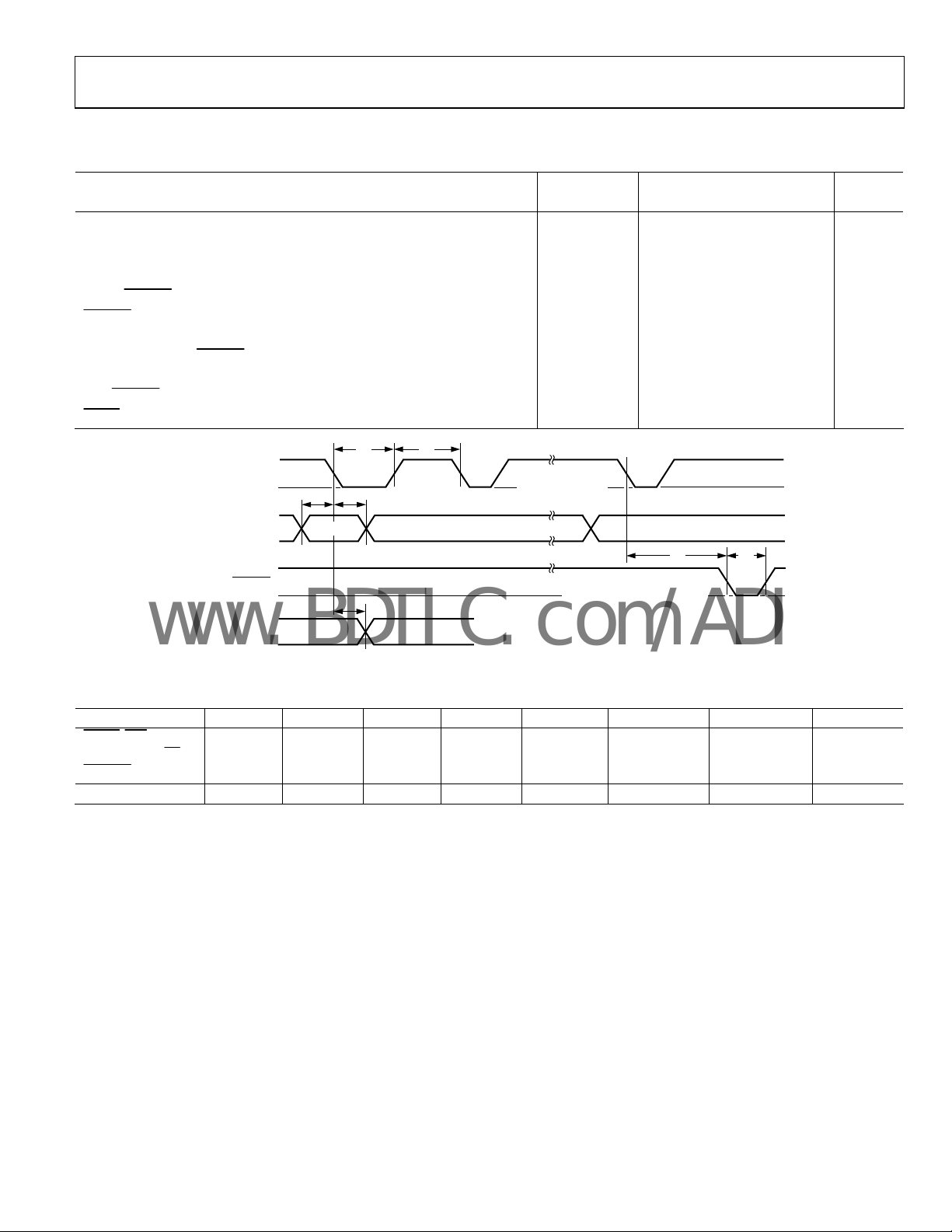
TIMING CHARACTERISTICS (SERIAL)
Table 2.
Limit
Parameter Symbol Min Typ Max Unit
Serial Data Setup Time t1 20 ns
CLK Pulse Width t2 100 ns
Serial Data Hold Time t3 20 ns
CLK Pulse Separation, Serial Mode t4 100 ns
t
CLK to UPDATE Delay
UPDATE Pulse Width
CLK to DATA OUT Valid, Serial Mode t7 200 ns
Propagation Delay, UPDATE to Switch On or Off
Data Load Time, CLK = 5 MHz, Serial Mode 16 μs
CLK, UPDATE Rise and Fall Times
RESET Time
0 ns
5
t
50 ns
6
50 ns
100 ns
200 ns
CLK
DATA IN
1 = LATCHED
UPDATE
0 = TRANSPARENT
DATA OUT
t
1
0
t1t
1
0
2
3
t
7
t
4
LOAD DATA INTO
SERIAL REGISTER
ON FALLING EDGE
TRANSFER DATA FROM SERIAL
LATCHES DURING LOW LEVEL
Figure 2. Timing Diagram, Serial Mode
OUT00 (D0)OUT07 (D3)OUT07 (D4)
t
5
REGISTER TO PARALLEL
t
6
6523-002
Table 3. Logic Levels
Pins VIH V
RESET, SER/PAR,
CLK, DATA IN, CE
2.0 V min 0.8 V max 20 μA max −400 μA min
,
VOH VOL IIH IIL IOH IOL
IL
UPDATE
DATA OUT 2.7 V min 0.5 V max −400 μA max 3.0 mA min
Rev. 0 | Page 5 of 28
AD8112
0
www.BDTIC.com/ADI
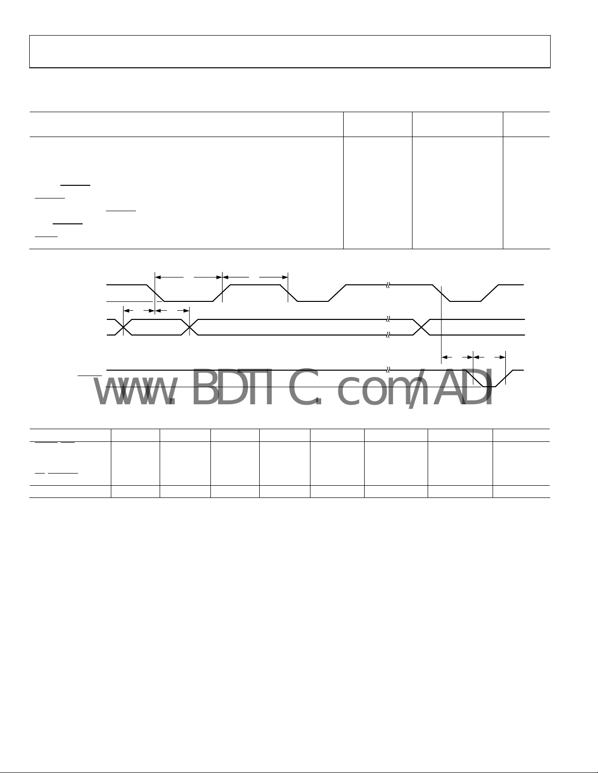
TIMING CHARACTERISTICS (PARALLEL)
Table 4.
Limit
Parameter Symbol Min Max Unit
Data Setup Time t1 20 ns
CLK Pulse Width t2 100 ns
Data Hold Time t3 20 ns
CLK Pulse Separation t4 100 ns
t
CLK to UPDATE Delay
UPDATE Pulse Width
Propagation Delay, UPDATE to Switch On or Off
CLK, UPDATE Rise and Fall Times
RESET Time
0 ns
5
t
50 ns
6
50 ns
100 ns
200 ns
t
4
Figure 3. Timing Diagram, Parallel Mode
t
5
t
6
6523-003
CLK
D0 TO D4
A0 TO A2
1=LATCHED
UPDATE
= TRANSPARENT
t
1
0
1
0
t
1
2
t
3
Table 5. Logic Levels
Pins VIH V
RESET, SER/PAR,
2.0 V min 0.8 V max 20 μA max −400 μA min
VOH VOL IIH IIL IOH IOL
IL
CLK, D0, D1, D2,
D3, D4, A0, A1, A2,
CE, UPDATE
DATA OUT 2.7 V min 0.5 V max −400 μA max 3.0 mA min
Rev. 0 | Page 6 of 28
AD8112
www.BDTIC.com/ADI
ABSOLUTE MAXIMUM RATINGS
Table 6.
Parameter Rating
Analog Supply Voltage (AVCC to AVEE) 26.0 V
Digital Supply Voltage (DVCC to DGND) 6 V
Ground Potential Difference (AGND to DGND) ±0.5 V
Internal Power Dissipation
Analog Input Voltage
Digital Input Voltage DVCC
Output Voltage (Disabled Output) (AVCC − 1.5 V) to
Output Short-Circuit Duration Momentary
Storage Temperature Range −65°C to +125°C
Lead Temperature (Soldering 10 sec) 300°C
1
Specification is for device in free air (TA = 25°C):
100-lead plastic LQFP (ST): θJA = 40°C/W.
2
To avoid differential input breakdown, ensure that one-half the output
voltage (1/2 V
differential. See Output Voltage Swing specification for linear output range.
) and any input voltage is less than 10 V of the potential
OUT
1
2
3.1 W
Maintain linear output
+ 1.5 V)
(AV
EE
Stresses above those listed under Absolute Maximum Ratings
may cause permanent damage to the device. This is a stress
rating only; functional operation of the device at these or any
other conditions above those indicated in the operational
section of this specification is not implied. Exposure to absolute
maximum rating conditions for extended periods may affect
device reliability.
POWER DISSIPATION
The AD8112 is operated with ±5 V to ±12 V supplies and can
drive loads down to 150 Ω (±5 V) or 600 Ω (±12 V), resulting
in a large range of possible power dissipations. For this reason,
extra care must be taken when derating the operating conditions
based on ambient temperature.
Packaged in a 100-lead LQFP, the AD8112 junction-to-ambient
hermal impedance (θ
t
the maximum allowed junction temperature of the plastic encapsulated die should not exceed 150°C. Temporarily exceeding
this limit may cause a shift in parametric performance due
to a change in the stresses exerted on the die by the package.
Exceeding a junction temperature of 175°C for an extended
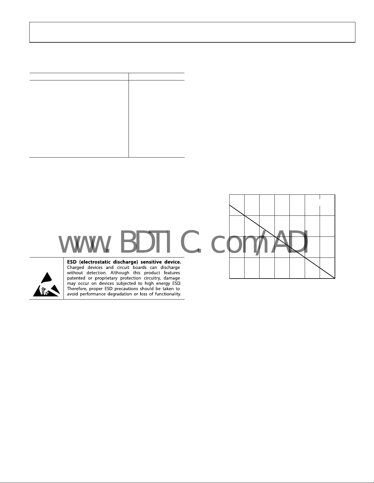
period can result in device failure. The curve in
he range of allowed power dissipations that meet these conditions
t
over the commercial range of ambient temperatures.
4.0
3.5
3.0
) is 40°C/W. For long-term reliability,
JA
Figure 4 shows
TJ= 150°C
ESD CAUTION
MAXIMUM POWER (W)
2.5
2.0
0 1020304050607
Figure 4. Maximum Power Dissipation vs. Ambient Temperature
AMBIENT T EMPERATURE (°C)
06523-004
0
Rev. 0 | Page 7 of 28
AD8112
www.BDTIC.com/ADI
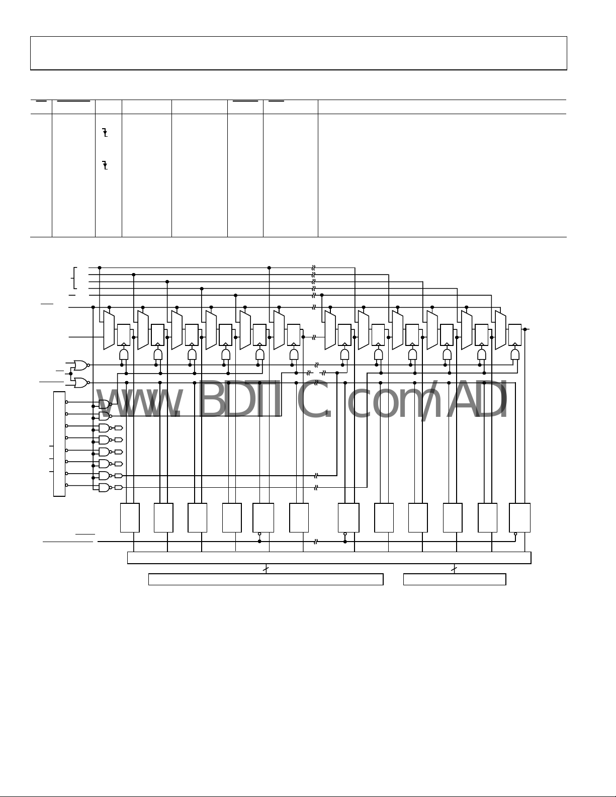
Table 7. Operation Truth Table
CE
UPDATE
CLK DATA IN DATA OUT
RESET
1 X X X X X X No change in logic.
0 1
0 1
Data
Data
i
D0 ... D4,
A0 ... A2
1 0
i-80
N/A in
Parallel
1 1
Mode
0 0 X X X 1 X
X X X X X 0 X
D0
DATA
D1
D2
D3
D4
D
CLK
S
D1
Q
Q
D0
S
D1
Q
D0
S
D1
D
QDQDQDQDQ DQ DQ DQ DQDQDQ
Q
D0
CLK
S
D1
Q
D0
CLK CLK CLK
S
D1
Q
D0
PARALLEL
(OUTPUT
ENABLE)
SER/PAR
DATA IN
(SERIAL)
SER
D1
D0
/PAR
S
Q
CLK
Operation/Comment
The data on the serial DATA IN line is loaded into serial register.
he first bit clocked into the serial register appears at DATA OUT
T
80 clocks later.
The data on the parallel data lines, D0 to D4, is loaded into the
80-bit serial shift register location addressed by A0 to A2.
Data in the 80-bit shift register transf
ers into the parallel
latches that control the switch array. Latches are transparent.
Asynchronous operation. All out
puts are disabled. Remainder
of logic is unchanged.
CLK
S
D1
Q
D0
S
D1
Q
D0
S
D1
Q
D0
CLK CLK CLK CLK
S
D1
Q
D0
S
D1
Q
D0
CLK
S
D1
Q
D0
DATA OUT
CLK
CE
UPDATE
OUT00 EN
OUT01 EN
OUT02 EN
OUTPUT
ADDRESS
OUT03 EN
OUT04 EN
A0
OUT05 EN
A1
3-TO- 16 DECODE R
OUT06 EN
A2
OUT07 EN
(OUTPUT ENABLE)
RESET
OUT00
B0
DLE
Q
OUT00
B1
DLE
Q
OUT00
B2
DLE
Q
OUT00
B3
DLE
Q
DLE
OUT00
EN
QCLR
128
SWITCH MATRIX
OUT01
B0
DLE
Q
DECODE
OUT06
EN
DLE
QCLR
OUT07
B0
DLE
Q
DLE
OUT07
B1
Q
OUTPUT ENABLE
OUT07
B2
DLE
Q
8
OUT07
B3
DLE
Q
OUT07
EN
DLE
QCLR
06523-005
Figure 5. Logic Diagram
Rev. 0 | Page 8 of 28
AD8112
www.BDTIC.com/ADI
PIN CONFIGURATION AND FUNCTION DESCRIPTIONS
RESETCEDATA OUT
CLK
DATA IN
UPDATE
100
SER/PARNCNCNCNCNCNCNCNCNCA0A1A2
99
97
98
93
95
96
929190
94
8988878685
84
83
82
DGNDD0D1D2D3
797877
81
80
D4
76
1
DV
CC
2
DGND
3
AGND
4
IN08
5
AGND
6
IN09
7
AGND
8
IN10
9
AGND
10
IN11
11
AGND
12
IN12
13
AGND
14
IN13
15
AGND
16
IN14
17
AGND
18
IN15
19
AGND
20
AV
EE
21
AV
CC
22
AV
CC
23
NC
24
AV
EE
25
NC
NC = NO CO NNECT
PIN 1
26
CC
AV
75
DV
CC
74
DGND
73
AGND
72
IN07
71
AGND
70
IN06
69
AGND
68
IN05
67
AGND
66
IN04
65
AD8112
TOP VIEW
(Not to Scale)
45
48
03/04
AV
49
47
02/03
OUT03
OUT02
EE
CC
AV
27
28
NC
AV
29
30
EE
CC
NC
AV
31NC32
AV
34
33
EE
NC
AV
36
35
EE
CC
NC
AV
37NC38
AV
40
41
42
39
CC
06/07
05/06
OUT06
OUT07
EE
CC
AV
AV
46
43
44
04/05
OUT05
OUT04
EE
AV
AGND
64
IN03
63
AGND
62
IN02
61
AGND
60
IN01
59
AGND
58
IN00
57
AGND
56
AV
EE
55
AV
CC
54
AVCC00
53
OUT00
52
AVEE00/01
51
OUT01
50
01/02
CC
AV
06523-006
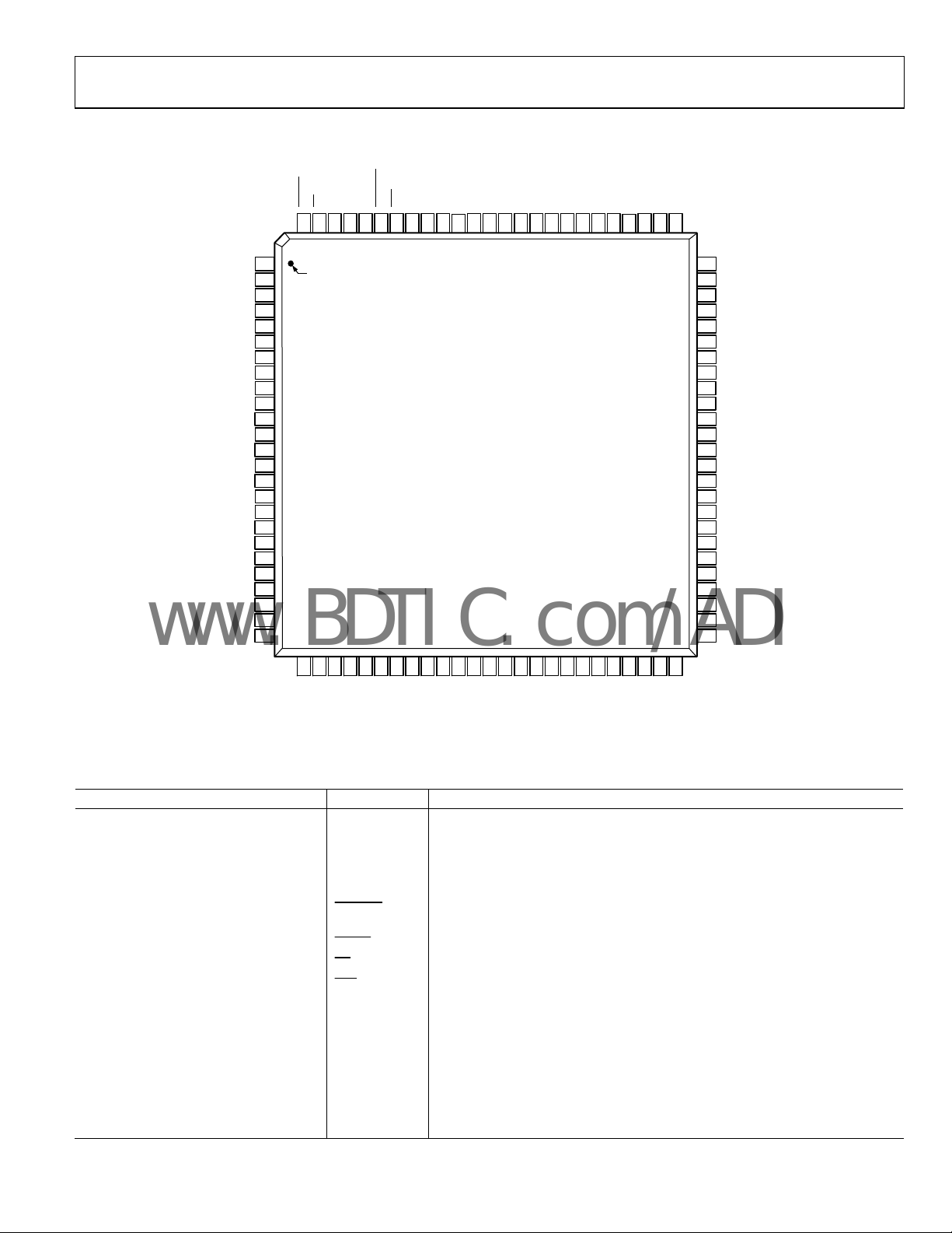
Figure 6. Pin Configuration
Table 8. Pin Function Descriptions
Pin No. Mnemonic Description
58, 60, 62, 64, 66, 68, 70, 72, 4, 6, 8, 10,
IN00 to IN15
1
Analog Inputs for Channel Numbers 00 through 15.
12, 14, 16, 18
96 DATA IN Serial Data Input, TTL-compatible.
97 CLK Clock, TTL-compatible. Falling edge triggered.
98 DATA OUT Serial Data Output, TTL-compatible.
95
UPDATE
Enable (Transparent) Low. Allows serial register to connect directly to switch
matrix. Data latched when high.
100
99
94
RESET
CE
/PAR Serial Data/Parallel Data. When low, this pin selects serial data mode; when
SER
Disable Outputs, Active Low.
Chip Enable, Enable Low. Must be low to clock in and latch data.
high, this pin selects parallel data mode, high. Must be connected.
53, 51, 49, 47, 45, 43, 41, 39
3, 5, 7, 9, 11, 13, 15, 17, 19, 57, 59, 61, 63,
OUT00 to
1
07
OUT
AGND Analog Ground for Inputs and S
Analog Outputs for Channel Numbers 00 Through 07.
witch Matrix. Must be connected.
65, 67, 69, 71, 73
1, 75 DVCC 5 V for Digital Circuitry.
2, 74, 81 DGND Ground for Digital Circuitry.
20, 24, 28, 32, 36, 56 AVEE −5 V for Inputs and Switch Matrix.
Rev. 0 | Page 9 of 28
 Loading...