Analog Devices AD8099 b Datasheet
Ultralow Distortion, High Speed
FEATURES
Ultralow noise: 0.95 nV/√Hz, 2.6 pA/√Hz
Ultralow distortion
nd
harmonic RL = 1 kΩ , G = +2
2
−92 dB @ 10 MHz
rd
3
harmonic RL = 1 kΩ , G = +2
−105 dB @ 10 MHz
High speed
GBWP: 3.8 GHz
–3 dB bandwidth:
700 MHz (G = +2)
550 MHz (G = +10)
Slew rate:
475 V/µs (G = +2)
1350 V/µs (G = +10)
New pinout
Custom external compensation, gain range –1, +2 to +10
Supply current: 15 mA
Offset voltage: 0.5 mV max
Wide supply voltage range: 5 V to 12 V
GENERAL DESCRIPTION
The AD8099 is an ultralow noise (0.95 nV/√Hz) and distortion
(–92 dBc @10 MHz) voltage feedback op amp, the combination
of which make it ideal for 16- and 18-bit systems. The AD8099
features a new, highly linear, low noise input stage that increases
the full power bandwidth (FPBW) at low gains with high slew
rates. ADI’s proprietary next generation XFCB process enables
such high performance amplifiers with relatively low power.
The AD8099 features external compensation, which lets the
user set the gain bandwidth product. External compensation
allows gains from +2 to +10 with minimal trade-off in bandwidth. The AD8099 also features an extremely high slew rate of
1350 V/µs, giving the designer flexibility to use the entire
dynamic range without trading off bandwidth or distortion.
The AD8099 settles to 0.1% in 18 ns and recovers from
overdrive in 50 ns.
The AD8099 drives 100 Ω loads at breakthrough performance
levels with only 15 mA of supply current. With the wide supply
voltage range (5 V to 12 V), low offset voltage (0.1 mV typ),
wide bandwidth (700 MHz for G = +2), and a GBWP up to
3.8 GHz, the AD8099 is designed to work in a wide variety of
applications.
0.95 nV/√Hz Voltage Noise Op Amp
AD8099
APPLICATIONS
Pre-amplifiers
Receivers
Instrumentation
Filters
IF and baseband amplifiers
A-to-D drivers
DAC buffers
Optical electronics
CONNECTION DIAGRAMS
–V
–IN
+IN
1
2
3
4
S
DISABLE
FEEDBACK
–IN
+IN
1
2
3
4
8
+V
S
7
V
OUT
6
C
C
5
–V
S
FEEDBACK
04511-0-001
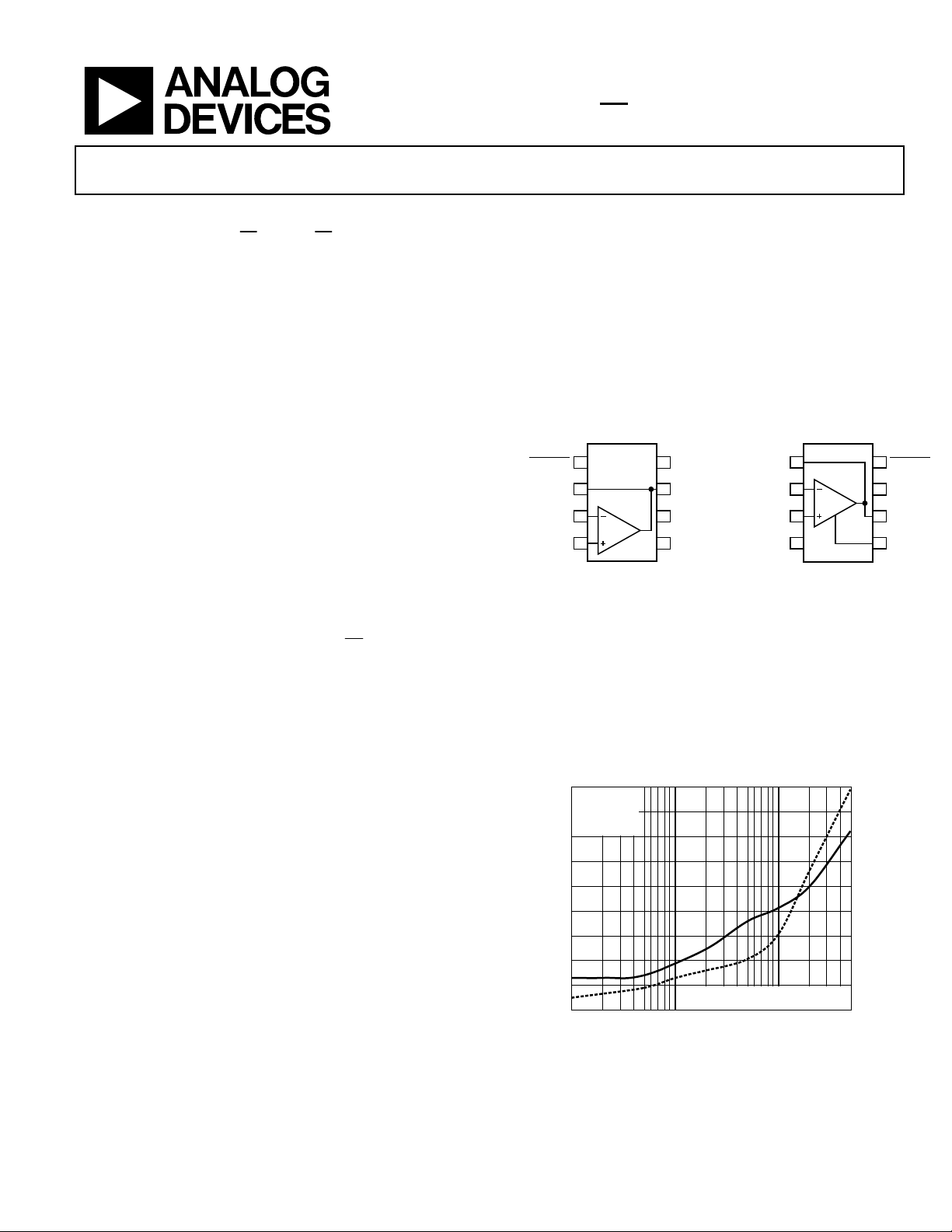
Figure 1. 8-Lead CSP (CP-8) Figure 2. 8-Lead SOIC-ED (RD-8)
The AD8099 is available in a 3 mm × 3 mm lead frame chip
scale package (LFCSP) with a new pinout that is specifically
optimized for high performance, high speed amplifiers. The
new LFCSP package and pinout enable the breakthrough
performance that previously was not achievable with amplifiers.
The AD8099 is rated to work over the extended industrial
temperature range, −40°C to +125°C.
–40
G = +2
= 2V p-p
V
OUT
–50
V
= ±5V
S
R
= 1kΩ
L
–60
–70
–80
–90
–100
–110
HARMONIC DISTORTION (dBc)
–120
–130
0.1 1.0 10.0
Figure 3 . Harmonic Distortion vs. Frequency and Gain (SOIC)
SOLID LINE – SECOND HARMONIC
DOTTED LINE – THIRD HARMONIC
FREQUENCY (MHz)
8
DISABLE
7
+V
6
V
5
C
04511-A-013
S
OUT
C
04511-0-002
Rev. B
Information furnished by Analog Devices is believed to be accurate and reliable.
However, no responsibility is assumed by Analog Devices for its use, nor for any
infringements of patents or other rights of third parties that may result from its use.
Specifications subject to change without notice. No license is granted by implication
or otherwise under any patent or patent rights of Analog Devices. Trademarks and
registered trademarks are the property of their respective owners.
One Technology Way, P.O. Box 9106, Norwood, MA 02062-9106, U.S.A.
Tel: 781.329.4700
Fax: 781.326.8703 © 2004 Analog Devices, Inc. All rights reserved.
www.analog.com

AD8099
TABLE OF CONTENTS
Specifications..................................................................................... 3
Specifications with ±5 V Supply................................................. 3
Specifications with +5 V Supply................................................. 4
Absolute Maximum Ratings............................................................ 5
Maximum Power Dissipation .....................................................5
ESD Caution.................................................................................. 5
Typical Performance Characteristics............................................. 6
Theory of Operation ...................................................................... 15
Applications..................................................................................... 16
Using the AD8099...................................................................... 16
Circuit Components...................................................................16
REVISION HISTORY
6/04—Data Sheet changed from REV. A to REV. B
Change to General Description...................................................... 1
Changes to Maximum Power Dissipation section ...................... 5
Changes to Applications section .................................................. 16
Changes to Table 7.......................................................................... 24
Changes to Ordering Guide.......................................................... 26
1/04—Data Sheet changed from REV. 0 to REV. A
Recommended Values ............................................................... 17
Circuit Configurations .............................................................. 17
Performance vs. Component values........................................ 19
Total Output Noise Calculations and Design......................... 20
Input Bias Current and DC Offset ........................................... 21
DISABLE
16-Bit ADC Driver..................................................................... 22
Circuit Considerations .............................................................. 23
Design Tools and Technical Support....................................... 23
Outline Dimensions .......................................................................25
Ordering Guide............................................................................... 26
Pin and Input Bias Cancellation............................. 21
Inserted new Figure 3................................................................... 1
Changes to Specifications............................................................ 3
Inserted new Figures 22 to 34..................................................... 8
Inserted new Figures 51 to 55................................................... 14
Changes to Theory of Operation section ................................16
Changes to Circuit Components section................................. 17
Changes to Table 4...................................................................... 18
Changes to Figure 60.................................................................. 18
Changes to Total Output Noise Calculations and
Design section........................................................................ 21
Changes to Figure 60.................................................................. 22
Changes to Figure 62.................................................................. 23
Changes to 16-Bit ADC Driver section................................... 23
Changes to Table 6...................................................................... 23
Additions to PCB Layout section ............................................. 23
11/03—Revision 0: Initial Version
Rev. B | Page 2 of 28
AD8099
SPECIFICATIONS
SPECIFICATIONS WITH ±5 V SUPPLY
TA = 25°C, G = +2, RL = 1 kΩ to ground, unless otherwise noted. Refer to Figure 60 through Figure 66 for component values and
gain configurations .
Table 1.
Parameter Conditions Min Typ Max Unit
DYNAMIC PERFORMANCE
–3 dB Bandwidth G = +5, V
G = +5, V
Bandwidth for 0.1 dB Flatness (SOIC/CSP) G = +2, V
Slew Rate G = +10, V
G = +2, V
Settling Time to 0.1% G = +2, V
NOISE/DISTORTION PERFORMANCE
Harmonic Distortion (dBc) HD2/HD3 fC = 500 kHz, V
f
= 10 MHz, V
C
Input Voltage Noise f = 100 kHz 0.95
Input Current Noise
f = 100 kHz,
f = 100 kHz,
DC PERFORMANCE
Input Offset Voltage 0.1 0.5 mV
Input Offset Voltage Drift 2.3 µV/°C
Input Bias Current
DISABLE
DISABLE
Input Bias Current Drift 3 nA/°C
Input Bias Offset Current 0.06 1 µA
Open-Loop Gain 82 85 dB
INPUT CHARACTERISTICS
Input Resistance Differential mode 4 kΩ
Common mode 10 MΩ
Input Capacitance 2 pF
Input Common-Mode Voltage Range –3.7 to +3.7 V
Common-Mode Rejection Ratio VCM = ±2.5 V 98 105 dB
DISABLE
PIN
DISABLE
Input Voltage
Turn-Off Time
Turn-On Tim e
Enable Pin Leakage Current
DISABLE
Pin Leakage Current
Output disabled <2.4 V
50% of
= 0.5 V, G = +2
V
IN
50% of
= 0.5 V, G = +2
V
IN
DISABLE
DISABLE
OUTPUT CHARACTERISTICS
Output Overdrive Recovery Time (Rise/Fall) V
= -2.5 V to 2.5 V, G =+2 30/50 ns
IN
Output Voltage Swing RL = 100 Ω –3.4 to +3.5 –3.6 to +3.7 V
R
= 1 kΩ –3.7 to +3.7 –3.8 to +3.8 V
L
Short-Circuit Current Sinking and sourcing 131/178 mA
Off Isolation
f = 1 MHz,
POWER SUPPLY
Operating Range ±5 ±6 V
Quiescent Current 15 16 mA
Quiescent Current (Disabled)
DISABLE
Positive Power Supply Rejection Ratio +VS = 4 V to 6 V, –VS = –5 V (input referred) 85 91 dB
Negative Power Supply Rejection Ratio +VS = 5 V, –VS = –6 V to –4 V (input referred) 86 94 dB
= 0.2 V p-p 450 510 MHz
OUT
= 2 V p-p 205 235 MHz
OUT
= 0.2 V p-p 34/25 MHz
OUT
= 6 V Step 1120 1350 V/µs
OUT
= 2 V Step 435 470 V/µs
OUT
= 2 V Step 18 ns
OUT
= 2 V p-p, G = +10 –102/–111 dBc
OUT
= 2 V p-p, G = +10 –84/–92 dBc
OUT
DISABLE
DISABLE
pin floating
pin = +V
DISABLE
to < 10% of final V
pin floating
pin = +V
S
S
,
OUT
2.6
5.2
–6 –13 µA
–0.1 –2 µA
105 ns
DISABLE
=+5 V
= –5 V
DISABLE
= Low
to < 10% of final V
= low
OUT
,
39 ns
17 21 µA
35 44 µA
–61 dB
1.7 2 mA
Hz
nV/√
pA/√Hz
Hz
pA/√
Rev. B | Page 3 of 28
AD8099
SPECIFICATIONS WITH +5 V SUPPLY
VS = 5 V @ TA = 25°C, G = +2, RL = 1 kΩ to midsupply, unless otherwise noted. Refer to Figure 60 through Figure 66 for component
values and gain configurations .
Table 2.
Parameter Conditions Min Typ Max Unit
DYNAMIC PERFORMANCE
–3 dB Bandwidth G = +5, V
G = +5, V
Bandwidth for 0.1 dB Flatness (SOIC/CSP) G = +2, V
Slew Rate G = +10, V
G = +2, V
Settling Time to 0.1% G = +2, V
NOISE/DISTORTION PERFORMANCE
Harmonic Distortion (dBc) HD2/HD3 fC = 500 kHz, V
f
= 10 MHz, V
C
Input Voltage Noise f = 100 kHz 0.95
Input Current Noise
f = 100 kHz,
f = 100 kHz,
DC PERFORMANCE
Input Offset Voltage 0.1 0.5 mV
Input Offset Voltage Drift 2.5 µV/°C
Input Bias Current
DISABLE
DISABLE
Input Bias Offset Current 0.05 1 µA
Input Bias Offset Current Drift 2.4 nA/°C
Open-Loop Gain V
OUT
INPUT CHARACTERISTICS
Input Resistance Differential mode 4 kΩ
Common mode 10 MΩ
Input Capacitance 2 pF
Input Common-Mode Voltage Range 1.3 to 3.7 V
Common-Mode Rejection Ratio VCM = 2 V to 3 V 88 105 dB
DISABLE
PIN
DISABLE
Input Voltage
Turn-Off Time
Turn-On Tim e
Enable Pin Leakage Current
DISABLE
Pin Leakage Current
Output disabled <2.4 V
50% of
= 0.5 V, G = +2
V
IN
50% of
= 0.5 V, G = +2
V
IN
DISABLE
DISABLE
OUTPUT CHARACTERISTICS
Overdrive Recovery Time (Rise/Fall) VIN = 0 to 2.5 V, G = +2 50/70 ns
Output Voltage Swing RL = 100 Ω 1.5 to 3.5 1.2 to 3.8 V
R
= 1 kΩ 1.2 to 3.8 1.2 to 3.8 V
L
Short-Circuit Current Sinking and Sourcing 60/80 mA
Off Isolation
f = 1 MHz,
POWER SUPPLY
Operating Range ±5 ±6 V
Quiescent Current 14.5 15.4 mA
Quiescent Current (Disabled)
DISABLE
Positive Power Supply Rejection Ratio +VS = 4.5 V to 5.5 V, –VS = 0 V (input referred) 84 89 dB
Negative Power Supply Rejection Ratio +VS =5 V, -VS= –0.5 V to +0.5 V (input referred) 84 90 dB
= 0.2 V p-p 415 440 MHz
OUT
= 2 V p-p 165 210 MHz
OUT
= 0.2 V p-p 33/23 MHz
OUT
= 2 V Step 630 715 V/µs
OUT
= 2 V Step 340 365 V/µs
OUT
= 2 V Step 18 ns
OUT
= 1 V p-p, G = +10 –82/–94 dBc
OUT
= 1 V p-p, G = +10 –80/–75 dBc
OUT
nV/√
DISABLE
DISABLE
pin floating
pin = +V
S
pin floating
pin = +V
S
2.6
5.2
pA/√Hz
pA/√
–6.2 –13 µA
–0.2 –2 µA
= 1 V to 4 V 76 81 dB
DISABLE
DISABLE
= 5 V
= 0 V
DISABLE
= Low
to <10% of Final V
to <10% of Final V
= Low
OUT
OUT
,
,
105 ns
61 ns
16 21 µA
33 44 µA
–61 dB
1.4 1.7 mA
Hz
Hz
Rev. B | Page 4 of 28
AD8099
(
)
(
ABSOLUTE MAXIMUM RATINGS
Table 3.
Parameter Rating
Supply Voltage 12.6 V
Power Dissipation See Figure 4
Differential Input Voltage ±1.8 V
Differential Input Current ±10mA
Storage Temperature –65°C to +125°C
Operating Temperature Range –40°C to +125°C
Lead Temperature Range (Soldering 10 sec) 300°C
Junction Temperature 150°C
Stresses above those listed under Absolute Maximum Ratings
may cause permanent damage to the device. This is a stress
rating only; functional operation of the device at these or any
other conditions above those indicated in the operational
section of this specification is not implied. Exposure to absolute
maximum rating conditions for extended periods may affect
device reliability.
The difference between the total drive power and the load
power is the drive power dissipated in the package.
PD = Quiescent Power + (Total Drive Power – Load Power)
⎛
V
()
D
⎜
IVP
SS
⎜
⎝
2
⎞
V
OUTS
⎟
×+×=
⎟
R
L
⎠
RMS output voltages should be considered. If
V
–, as in single-supply operation, then the total drive power is
S
V
× I
. If the rms signal levels are indeterminate, consider the
S
OUT
V
worst case, when
()
D
In single-supply operation with
is
V
= VS/2.
OUT
= VS/4 for RL to midsupply:
OUT
2
)
4
/V
S
+×=
IVP
SS
R
L
R
L
2
V
OUT
–
R
L
R
is referenced to
L
referenced to VS–, worst case
MAXIMUM POWER DISSIPATION
The maximum safe power dissipation in the AD8099 package is
limited by the associated rise in junction temperature (TJ) on
the die. The plastic encapsulating the die will locally reach the
junction temperature. At approximately 150°C, which is the
glass transition temperature, the plastic will change its
properties. Even temporarily exceeding this temperature limit
may change the stresses that the package exerts on the die,
permanently shifting the parametric performance of the
AD8099. Exceeding a junction temperature of 150°C for an
extended period can result in changes in silicon devices,
potentially causing failure.
× I
OUT
),
JA
).
The still-air thermal properties of the package and PCB (θ
the ambient temperature (T
the package (P
) determine the junction temperature of the die.
D
), and the total power dissipated in
A
The junction temperature can be calculated as
θPTT ×+=
J
The power dissipated in the package (
D
A
JA
P
) is the sum of the
D
quiescent power dissipation and the power dissipated in the
package due to the load drive for all outputs. The quiescent
V
power is the voltage between the supply pins (
I
quiescent current (
midsupply, the total drive power is
). Assuming the load (RL) is referenced to
S
V
/2 × I
S
dissipated in the package and some in the load (
) times the
S
, some of which is
OUT
V
OUT
Airflow will increase heat dissipation, effectively reducing θ
.
JA
Also, more metal directly in contact with the package leads
from metal traces, through holes, ground, and power planes will
reduce the θ
. Soldering the exposed paddle to the ground
JA
plane significantly reduces the overall thermal resistance of the
package. Care must be taken to minimize parasitic capacitances at the input leads of high speed op amps, as discussed in
the PCB Layout section.
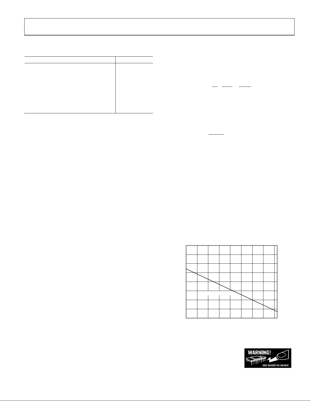
Figure 4 shows the maximum safe power dissipation in the
package versus the ambient temperature for the exposed paddle
(e-pad) SOIC-8 (70°C/W), and CSP (70°C/W), packages on a
JEDEC standard 4-layer board. θ
4.0
3.5
3.0
2.5
2.0
1.5
1.0
0.5
MAXIMUM POWER DISSIPATION (Watts)
0.0
LFCSP AND SOIC
AMBIENT TEMPERATURE (°C)
Figure 4. Maximum Power Dissipation
values are approximations.
JA
120–40 –20 0 20 40 60 80 100
04511-0-115
ESD CAUTION
ESD (electrostatic discharge) sensitive device. Electrostatic charges as high as 4000 V readily accumulate on
the human body and test equipment and can discharge without detection. Although this product features
proprietary ESD protection circuitry, permanent damage may occur on devices subjected to high energy
electrostatic discharges. Therefore, proper ESD precautions are recommended to avoid performance
degradation or loss of functionality.
Rev. B | Page 5 of 28
AD8099
TYPICAL PERFORMANCE CHARACTERISTICS
Default Conditions: VS = ±5 V, TA = 25°C, RL = 1 kΩ tied to ground unless otherwise noted. Refer to Figure 63 through Figure 66 for
component values and gain configurations.
4
3
2
1
0
–1
–2
–3
–4
–5
–6
–7
–8
NORMALIZED CLOSED-LOOP GAIN (dB)
–9
–10
1
V
V
R
OUT
= ±5V
S
LOAD
= 0.2V p-p
= 1kΩ
10 100 1000
FREQUENCY (MHz)
G = +2
G = +5
G = +20
G = +10
G = –1
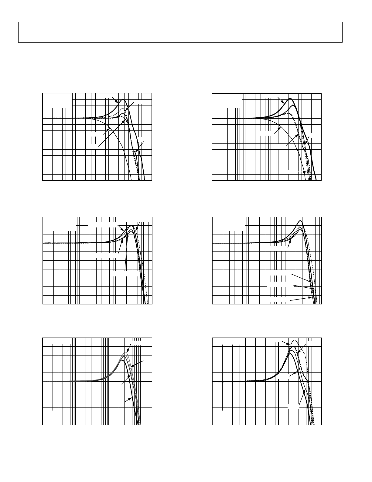
Figure 5. Small Signal Frequency Response for Various Gains (SOIC)
04511-0-074
4
3
2
1
0
–1
–2
–3
–4
–5
–6
–7
–8
NORMALIZED CLOSED-LOOP GAIN (dB)
–9
–10
1
V
V
R
OUT
S
LOAD
= 0.2V p-p
= ±5V
= 1kΩ
10 100 1000
G = +2
G = +20
G = –1
FREQUENCY (MHz)
G = +5
G = +10
Figure 8. Small Signal Frequency Response for Various Gains (CSP)
04511-0-073
17
G = +5
V
= ±5V
S
16
V
= 0.2V p-p
OUT
15
14
13
12
11
10
CLOSED-LOOP GAIN (dB)
9
8
7
1
RL = 100Ω, CSP
RL = 1kΩ, SOIC
10 100 1000
FREQUENCY (MHz)
RL = 1kΩ, CSP
RL = 100Ω, SOIC
04511-0-076
Figure 6. Small Signal Frequency Response for Various Load Resistors
11
V
= 0.2V p-p
OUT
10
9
8
7
6
5
4
CLOSED-LOOP GAIN (dB)
3
G = +2
2
= ±5V
V
S
R
= 1kΩ
L
1
FREQUENCY (MHz)
+25°C
+125°C
+85°C
–40°C
10001 10 100
04511-0-098
Figure 7. Small Signal Frequency Response for Various Temperatures (SOIC)
17
G = +5
R
= 1kΩ
L
16
V
= 0.2V p-p
OUT
15
14
13
12
11
10
CLOSED-LOOP GAIN (dB)
9
8
7
1
VS = ±5V, SOIC
VS = ±2.5V, CSP
VS = ±5V, CSP
VS = ±2.5V, SOIC
10 100 1000
FREQUENCY (MHz)
04511-0-077
Figure 9. Small Signal Frequency Response for Various Supply Voltages
11
V
= 0.2V p-p
OUT
10
9
8
7
6
5
4
CLOSED-LOOP GAIN (dB)
3
G = +2
2
V
= ±5V
S
= 1kΩ
R
L
1
FREQUENCY (MHz)
+125°C
–40°C
+25°C
+85°C
10001 10 100
04511-0-097
Figure 10. Small Signal Frequency Response for Various Temperatures (CSP)
Rev. B | Page 6 of 28
AD8099
20
G = +5
VS = ±5V
19
18
17
16
15
14
13
12
CLOSED-LOOP GAIN (dB)
11
10
9
1
10 100 1000
FREQUENCY (MHz)
5pF, CSP
1pF, SOIC
1pF, CSP
5pF, SOIC
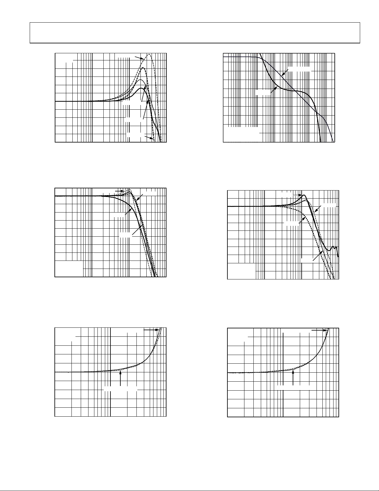
Figure 11. Small Signal Frequency Response for Various Capacitive Loads
1
0
–1
–2
–3
–4
–5
–6
–7
–8
VS = ±5V
V
= 2V p-p
–9
NORMALIZED CLOSED-LOOP GAIN (dB)
OUT
= 1k
LOAD
Ω
R
–10
1 10 100 1000
G = +2
G = +20
G = +5
FREQUENCY (MHz)
G = +10
04511-0-104
04511-0-011
90
80
70
60
50
40
30
20
OPEN-LOOP GAIN (dB)
10
VS = ±5V
0
= 1kΩ
R
L
UNCOMPENSATED
–10
0.001 0.01 0.1 1.0 10 100 1000
PHASE
FREQUENCY (MHz)
Figu nse
re 14. Open Loop Frequency Respo
MAGNITUDE
2
1
0
–1
–2
–3
–4
–5
–6
–7
VS = ±5V
= 2V p-p
V
–8
NORMALIZED CLOSED-LOOP GAIN (dB)
OUT
= 1k
LOAD
Ω
R
–9
1 10 100 1000
G = +2
G = +20
G = +5
FREQUENCY (MHz)
G = +10
–30
–45
–60
–75
–90
–105
–120
–135
–150
–165
–180
OPEN-LOOP PHASE (Degrees)
04511-0-012
04511-0-080
Figure 12. Large Signal Frequency Response for Various Gains (SOIC)
6.5
VS = ±5V
G = +2
6.4
= 150
Ω
R
L
6.3
6.2
6.1
6.0
5.9
5.8
CLOSED-LOOP GAIN (dB)
5.7
5.6
5.5
1
FREQUENCY (MHz)
V
= 1.4V p-p
OUT
V
= 200mV p-p
OUT
10 100
Figure 13. 0.1 dB latness (SOIC) F
04511-0-009
Rev. B | Page 7 of 28
Figure 15. Large Signal Frequency Response for Various Gains (CSP)
6.5
VS = ±5V
G = +2
6.4
= 150
Ω
R
L
6.3
6.2
6.1
6.0
5.9
5.8
CLOSED-LOOP GAIN (dB)
5.7
5.6
5.5
1
V
= 1.4V p-p
OUT
V
= 200mV p-p
OUT
10 100
FREQUENCY (MHz)
Figure 16. 0.1 d Flatness (CSP) B
04511-0-008
AD8099
15
14
13
12
11
10
9
8
CLOSED-LOOP GAIN (dB)
7
G = +5
6
VS = ±5V
= 2V p-p
V
OUT
5
1
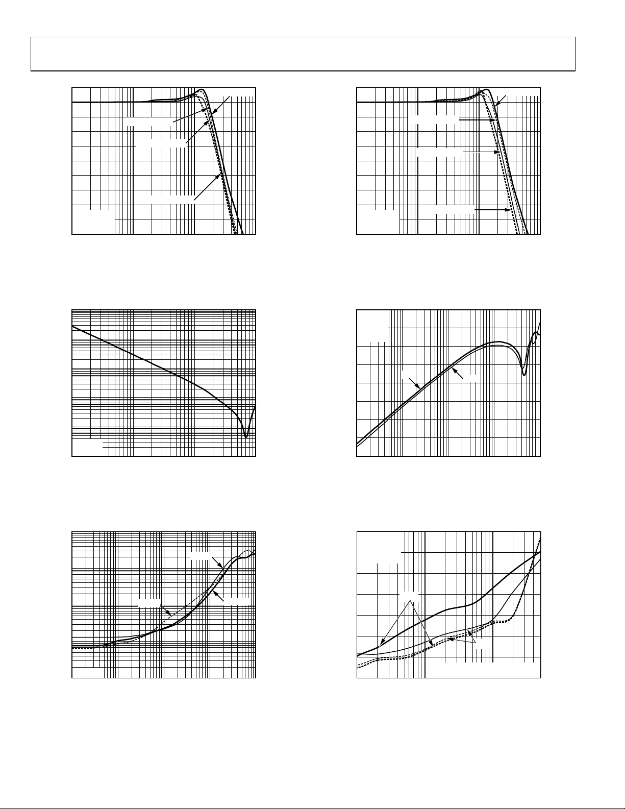
Figure 17. Large Sign us Load Resistances
RL = 100Ω, CSP
RL = 100Ω, SOIC
RL = 1kΩ, SOIC
10 100 1000
FREQUENCY (MHz)
al Frequency Response for Vario
100.0
10.0
RL = 1kΩ, CSP
04511-0-078
15
14
13
12
11
10
9
8
CLOSED-LOOP GAIN (dB)
7
G = +5
6
R
= 1k
Ω
L
V
= 2V p-p
OUT
5
1
Figu es
re 20. Large Signal Frequency Response for Various Supply Voltag
VS = ±2.5V, CSP
VS = ±5V, SOIC
VS = ±2.5V, SOIC
10 100 1000
FREQUENCY (MHz)
VS = ±5V, CSP
–10
G = +2
R
= 1kΩ
L
–20
V
= ±5V
S
V
= 0V
DIS
–30
04511-0-079
1.0
0.1
INPUT IMPEDANCE (kΩ)
0.01
VS = ±5V
G = +2
0.001
1
10 100 1000
Figure 18. Input Impedance vs. Frequency
100
10
)
Ω
1
0.1
OUTPUT IMPEDANCE (
VS = ±5V
0.01
Figure 19. Output Impedance . Frequency for Various Gains vs
FREQUENCY (MHz)
G = +2
FREQUENCY (MHz)
G = +5
G = +10
1000.1 1 10 1000
04511-0-105
04511-0-100
–40
–50
–60
OFF ISOLATION (dB)
–70
–80
–90
0.1
CSP
1 10 100 1000
FREQUENCY (MHz)
Figure 21. Off Isolation vs. Frequency
–50
G = +5
= 2V p-p
V
OUT
V
= ±5V
S
–60
= 100Ω
R
L
–70
–80
–90
–100
HARMONIC DISTORTION (dBc)
–110
–120
0.1 1.0 10.0
SOIC
SOLID LINES – SECOND HARMONICS
SOLID LINES – SECOND HARMONICS
DOTTED LINE – THIRD HARMONICS
FREQUENCY (MHz)
Figure 22. Harmonic D tion vs. Frequency istor
SOIC
CSP
04511-0-094
RMONICSDOTTED LINES– THIRD HA
04511-A-008
Rev. B | Page 8 of 28
AD8099
–50
–60
–70
G = +5
V
OUT
V
= ±5V
S
R
= 1kΩ
L
= 2V p-p
–50
–60
–70
G = +5
V
OUT
V
= ±5V
S
R
= 1kΩ
L
= 2V p-p
–80
–90
–100
–110
HARMONIC DISTORTION (dBc)
–120
–130
0.1 1.0 10.0
Fig C)
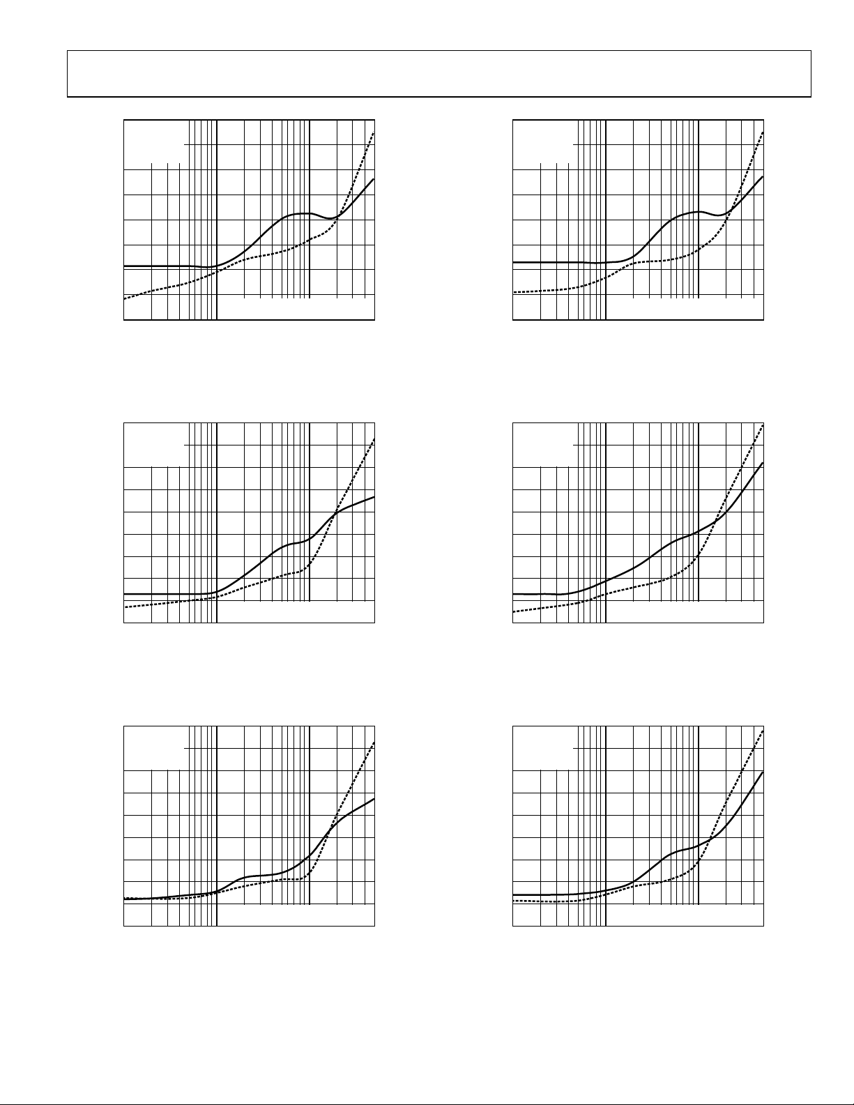
ure 23. Harmonic Distortion vs. Frequency (SOI
SOLID LINE – SECOND HARMONIC
DOTTED LINE – THIRD HARMONIC
FREQUENCY (MHz)
–40
G = +2
V
= 2V p-p
OUT
–50
V
= ±5V
S
R
= 1kΩ
L
–60
–70
–80
–90
–100
–110
HARMONIC DISTORTION (dBc)
–120
–130
0.1 1.0 10.0
Figure 24. Harmonic Disto tion vs. Frequency (SOIC)
SOLID LINES – SECOND HARMONICS
SOLID LINE – SECOND HARMONIC
DOTTED LINE – THIRD HARMONICS
FREQUENCY (MHz)
r
–40
G = –1
= 2V p-p
V
OUT
–50
V
= ±5V
S
R
= 1kΩ
L
–60
–70
–80
–90
–100
–110
HARMONIC DISTORTION (dBc)
–120
–130
0.1 1.0 10.0
SOLID LINE – SECOND HARMONIC
DOTTED LINE – THIRD HARMONIC
FREQUENCY (MHz)
Figure 25. Harmonic Disto tion vs. Frequency (SOIC) r
–80
–90
–100
–110
HARMONIC DISTORTION (dBc)
–120
–130
0.1 1.0 10.0
04511-A-009
SOLID LINE – SECOND HARMONIC
DOTTED LINE – THIRD HARMONIC
FREQUENCY (MHz)
04511-A-012
Figure 26. Harmonic Distortion vs. Frequency (CSP)
–40
G = +2
V
= 2V p-p
OUT
–50
V
= ±5V
S
R
= 1kΩ
L
–60
–70
–80
–90
–100
–110
HARMONIC DISTORTION (dBc)
–120
CDOTTED LINE – THIRD HARMONI
04511-A-010
–130
0.1 1.0 10.0
SOLID LINE – SECOND HARMONIC
DOTTED LINE – THIRD HARMONIC
FREQUENCY (MHz)
04511-A-013
Figure 27. Harmonic Distortion vs. Frequency (CSP)
–40
G = –1
= 2V p-p
V
OUT
–50
V
= ±5V
S
R
= 1kΩ
L
–60
–70
–80
–90
–100
–110
HARMONIC DISTORTION (dBc)
–120
–130
04511-A-011
0.1 1.0 10.0
SOLID LINE – SECOND HARMONIC
DOTTED LINE – THIRD HARMONIC
FREQUENCY (MHz)
04511-A-014
Figure 28. Harmonic Distortion vs. Frequency (CSP)
Rev. B | Page 9 of 28
 Loading...