Analog Devices AD8029 30 40 a Datasheet

Low Power, High Speed
FEATURES
Low power
1.3 mA supply current/amplifier
High speed
125 MHz, –3 dB bandwidth (G = +1)
60 V/µs slew rate
80 ns settling time to 0.1%
Rail-to-rail input and output
No phase reversal, inputs 200 mV beyond rails
Wide supply range: 2.7 V to 12 V
Offset voltage: 6 mV max
Low input bias current
+0.7 µA to –1.5 µA
Small packaging
SOIC-8, SC70-6, SOT23-8, SOIC-14, TSSOP-14
APPLICATIONS
Battery-powered instrumentation
Filters
A-to-D drivers
Buffering
GENERAL DESCRIPTION
The AD8029 (single), AD8030 (dual), and AD8040 (quad) are
rail-to-rail input and output high speed amplifiers with a
quiescent current of only 1.3 mA per amplifier. Despite their
low power consumption, the amplifiers provide excellent
performance with 125 MHz small signal bandwidth and
60 V/µs slew rate. ADI’s proprietary XFCB process enables high
speed and high performance on low power.
This family of amplifiers exhibits true single-supply operation
with rail-to-rail input and output performance for supply
voltages ranging from 2.7 V to 12 V. The input voltage range
extends 200 mV beyond each rail without phase reversal. The
dynamic range of the output extends to within 40 mV of each
rail.
The AD8029/AD8030/AD8040 provide excellent signal quality
with minimal power dissipation. At G = +1, SFDR is –72 dBc at
1 MHz and settling time to 0.1% is only 80 ns. Low distortion
and fast settling performance make these amplifiers suitable
drivers for single-supply A/D converters.
The versatility of the AD8029/AD8030/AD8040 allows the user
to operate the amplifiers on a wide range of supplies while
consuming less than 6.5 mW of power. These features extend
the operation time in applications ranging from battery-
Rev. A
Information furnished by Analog Devices is believed to be accurate and reliable.
However, no responsibility is assumed by Analog Devices for its use, nor for any
infringements of patents or other rights of third parties that may result from its use.
Specifications subject to change without notice. No license is granted by implication
or otherwise under any patent or patent rights of Analog Devices. Trademarks and
registered trademarks are the property of their respective owners.
Rail-to-Rail Input/Output Amplifier
AD8029/AD8030/AD8040
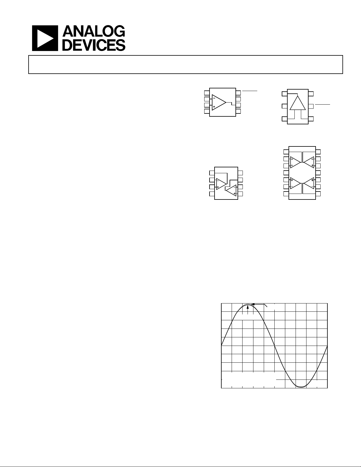
CONNECTION DIAGRAMS
1
NC
–IN
2
+IN
3
–V
4
S
NC = NO CONNECT
Figure 1. SOIC-8 (R)
1
V
1
OUT
–IN 1
2
+IN 1
3
4
–V
S
Figure 3. SOIC-8(R) and
SOT23-8 (RJ)
powered systems with large bandwidth requirements to high
speed systems where component density requires lower power
dissipation.
The AD8029/AD8030 are the only low power, rail-to-rail input
and output high speed amplifiers available in SOT23 and SC70
micro packages. The amplifiers are rated over the extended
industrial temperature range, –40°C to +125°C.
5.0
4.5
4.0
3.5
3.0
2.5
2.0
VOLTAGE (V)
1.5
1.0
0.5
0
One Technology Way, P.O. Box 9106, Norwood, MA 02062-9106, U.S.A.
Tel: 781.329.4700
Fax: 781.326.8703 © 2003 Analog Devices, Inc. All rights reserved.
8
DISABLE
+V
7
6
V
5
NC
S
OUT
V
1
OUT
–V
2
S
3
+IN
03679-A-004
+–
6
5
4
Figure 2. SC70-6 (KS)
V
1
1
OUT
–IN 1
2
+IN 1
3
4
8
+V
S
7
+V
2
OUT
–IN 2
6
5
+IN 2
+V
S
+IN 2
5
–IN 2
6
V
2
7
OUT
03679-A-003
Figure 4. SOIC-14 (R) and
TSSOP-14 (RU)
INPUT
OUTPUT
G = +1
V
= +5V
S
R
= 1kΩ TIED TO MIDSUPPLY
L
TIME (µs)
03679-A-010
Figure 5. Rail-to-Rail Response
www.analog.com
+V
S
DISABLE
–IN
14
V
OUT
13
–IN 4
+IN 4
12
11
–V
10
+IN 3
–IN 3
9
V
8
OUT
1µs/DIV
03679-A-002
4
S
3
03679-A-001

AD8029/AD8030/AD8040
TABLE OF CONTENTS
Specifications..................................................................................... 3
Specifications with ±5 V Supply ................................................. 3
Specifications with +5 V Supply ................................................. 4
Specifications with +3 V Supply ................................................. 5
Absolute Maximum Ratings............................................................ 6
Maximum Power Dissipation ..................................................... 6
Typical Performance Characteristics ............................................. 7
Theory of Operation ...................................................................... 15
Input Stage................................................................................... 15
Output Stage................................................................................ 15
Applications..................................................................................... 16
Wideband Operation................................................................. 16
Output Loading sensitivity........................................................ 16
Disable Pin .................................................................................. 17
Circuit Considerations .............................................................. 18
Design Tools and Technical Support....................................... 18
Outline Dimensions....................................................................... 19
Ordering Guide............................................................................... 20
ESD Caution................................................................................ 20
REVISION HISTORY
Revision A
11/03—Data Sheet Changed from Rev. 0 to Rev. A
Change Page
Added AD8040 part .......................................................Universal
Change to Figure 5 ....................................................................... 1
Changes to Specifications............................................................ 3
Changes to Figures 10–12............................................................ 7
Change to Figure 14 ..................................................................... 8
Changes to Figures 20 and 21 ..................................................... 9
Inserted new Figure 36............................................................... 11
Change to Figure 40 ................................................................... 12
Inserted new Figure 41............................................................... 12
Added Output Loading Sensitivity section............................. 16
Changes to Table 5...................................................................... 17
Changes to Power Supply Bypassing section .......................... 18
Changes to Ordering Guide...................................................... 20
Rev. A | Page 2 of 20

AD8029/AD8030/AD8040
SPECIFICATIONS
SPECIFICATIONS WITH ±5 V SUPPLY
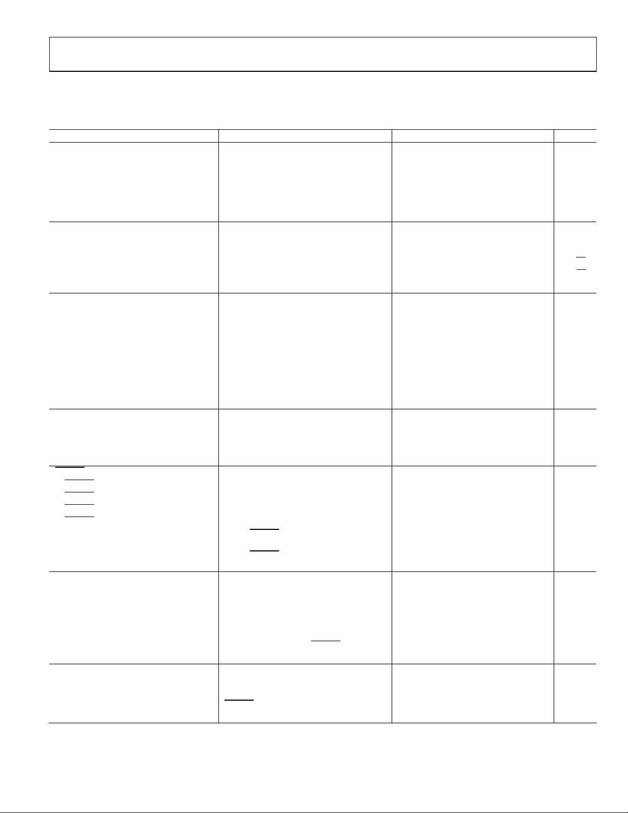
Table 1. VS = ±5 V @ TA = 25°C, G = +1, RL = 1 kΩ to ground, unless otherwise noted. All specifications are per amplifier.
Parameter Conditions Min Typ Max Unit
DYNAMIC PERFORMANCE
–3 dB Bandwidth G = +1, VO = 0.1 V p-p 80 125 MHz
G = +1, VO = 2 V p-p 14 19 MHz
Bandwidth for 0.1 dB Flatness G = +2, VO = 0.1 V p-p 6 MHz
Slew Rate G = +1, VO = 2 V Step 62 V/µs
G = –1, VO = 2 V Step 63 V/µs
Settling Time to 0.1% G = +2, VO = 2 V Step 80 ns
NOISE/DISTORTION PERFORMANCE
Spurious Free Dynamic Range (SFDR) fC = 1 MHz, VO = 2 V p-p –74 dBc
f
Input Voltage Noise f = 100 kHz 16.5
Input Current Noise f = 100 kHz 1.1
Crosstalk (AD8030/AD8040) f = 5 MHz, VIN = 2 V p-p
DC PERFORMANCE
Input Offset Voltage PNP Active, VCM = 0 V 1.6 5 mV
NPN Active, VCM = 4.5 V 2 6 mV
Input Offset Voltage Drift T
Input Bias Current
1
T
PNP Active, VCM = 0 V –1.7 –2.8 µA
T
Input Offset Current ±0.1 ±0.9 µA
Open-Loop Gain Vo = ±4.0 V 65 74 dB
INPUT CHARACTERISTICS
Input Resistance 6 MΩ
Input Capacitance 2 pF
Input Common-Mode Voltage Range –5.2 to +5.2 V
Common-Mode Rejection Ratio VCM = –4.5 V to +3 V, RL = 10 kΩ 80 90 dB
DISABLE
PIN (AD8029)
DISABLE
Low Voltage
DISABLE
Low Current
DISABLE
High Voltage
DISABLE
High Current
Turn-Off Time
Turn-On Time
OUTPUT CHARACTERISTICS
Output Overdrive Recovery Time
(Rising/Falling Edge) VIN = +6 V to –6 V, G = –1 55/45 ns
Output Voltage Swing RL = 1 kΩ –VS + 0.22 +VS – 0.22 V
R
Short-Circuit Current Sinking and Sourcing 170/160 mA
Off Isolation (AD8029)
Capacitive Load Drive 30% Overshoot 20 pF
POWER SUPPLY
Operating Range 2.7 12 V
Quiescent Current/Amplifier 1.4 1.5 mA
Quiescent Current (Disabled) DISABLE
Power Supply Rejection Ratio Vs ± 1 V 73 80 dB
1
Plus, +, (or no sign) indicates current into pin; minus (–) indicates current out of pin.
= 5 MHz, VO = 2 V p-p –56 dBc
C
Hz
nV/√
Hz
pA/√
dB
MIN
to T
MAX
–79
30 µV/°C
NPN Active, VCM = 4.5 V 0.7 1.3 µA
MIN
MIN
to T
to T
MAX
MAX
1 µA
2 µA
–V
+ 0.8 V
S
–6.5 µA
–V
+ 1.2 V
S
0.2 µA
DISABLE
50% of
VIN = –1 V, G = –1
DISABLE
50% of
to <10% of Final VO,
to <10% of Final VO,
150 ns
85 ns
VIN = –1 V, G = –1
= 10 kΩ –VS + 0.05 +VS – 0.05 V
L
V
= 0.1 V p-p, f = 1 MHz,
IN
= Low
DISABLE
= Low
–55 dB
150 200 µA
Rev. A | Page 3 of 20

AD8029/AD8030/AD8040
SPECIFICATIONS WITH +5 V SUPPLY
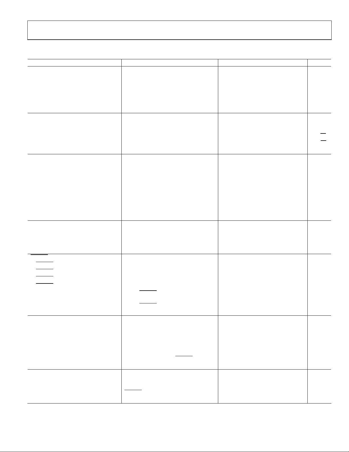
Table 2. VS = 5 V @ TA = 25°C, G = +1, RL = 1 kΩ to midsupply, unless otherwise noted. All specifications are per amplifier.
Parameter Conditions Min Typ Max Unit
DYNAMIC PERFORMANCE
–3 dB Bandwidth G = +1, VO = 0.1 V p-p 80 120 MHz
G = +1, VO = 2 V p-p 13 18 MHz
Bandwidth for 0.1 dB Flatness G = +2, VO = 0.1 V p-p 6 MHz
Slew Rate G = +1, VO = 2 V Step 55 V/µs
G = –1, VO = 2 V Step 60 V/µs
Settling Time to 0.1% G = +2, VO = 2 V Step 82 ns
NOISE/DISTORTION PERFORMANCE
Spurious Free Dynamic Range (SFDR) fC = 1 MHz, VO = 2 V p-p –73 dBc
f
Input Voltage Noise f = 100 kHz 16.5
Input Current Noise f = 100 kHz 1.1
Crosstalk (AD8030/AD8040) f = 5 MHz, VIN = 2 V p-p -79 dB
DC PERFORMANCE
Input Offset Voltage PNP Active, VCM = 2.5 V 1.4 5 mV
NPN Active, VCM = 4.5 V 1.8 6 mV
Input Offset Voltage Drift T
Input Bias Current
1
T
T
Input Offset Current ±0.1 ±0.9 µA
Open-Loop Gain Vo = 1 V to 4 V 65 74 dB
INPUT CHARACTERISTICS
Input Resistance 6 MΩ
Input Capacitance 2 pF
Input Common-Mode Voltage Range –0.2 to +5.2 V
Common-Mode Rejection Ratio VCM = 0.25 V to 2 V, RL = 10 kΩ 80 90 dB
DISABLE
PIN (AD8029)
DISABLE
DISABLE
DISABLE
DISABLE
Low Voltage
Low Current
High Voltage
High Current
Turn-Off Time
Turn-On Time
OUTPUT CHARACTERISTICS
Overdrive Recovery Time
(Rising/Falling Edge) VIN = –1 V to +6 V, G = –1 45/50 ns
Output Voltage Swing RL = 1 kΩ –VS + 0.17 +VS – 0.17 V
R
Short-Circuit Current Sinking and Sourcing 95/60 mA
Off Isolation (AD8029)
Capacitive Load Drive 30% Overshoot 15 pF
POWER SUPPLY
Operating Range 2.7 12 V
Quiescent Current/Amplifier 1.3 1.5 mA
Quiescent Current (Disabled)
Power Supply Rejection Ratio VS ± 1 V 73 80 dB
1
Plus, +, (or no sign) indicates current into pin; minus (–) indicates current out of pin.
= 5 MHz, VO = 2 V p-p –55 dBc
C
Hz
nV/√
Hz
pA/√
to T
MIN
25 µV/°C
MAX
NPN Active, VCM = 4.5 V 0.8 1.2 µA
to T
MIN
1 µA
MAX
PNP Active, VCM = 2.5 V –1.8 –2.8 µA
to T
MIN
2 µA
MAX
–V
+ 0.8 V
S
–6.5 µA
–V
+ 1.2 V
S
0.2 µA
DISABLE
50% of
VIN = –1 V, G = –1
DISABLE
50% of
VIN = –1 V, G = –1
= 10 kΩ –VS + 0.04 +VS – 0.04 V
L
= 0.1 V p-p, f = 1 MHz,
V
in
DISABLE
to <10% of Final VO,
to <10% of Final VO,
= Low
DISABLE
= Low
–55 dB
140 200 µA
155
ns
90
ns
Rev. A | Page 4 of 20

AD8029/AD8030/AD8040
SPECIFICATIONS WITH +3 V SUPPLY
Table 3. VS = +3 V @ TA = 25°C, G = +1, RL = 1 kΩ to midsupply, unless otherwise noted. All specifications are per amplifier.
Parameter Conditions Min Typ Max Unit
DYNAMIC PERFORMANCE
–3 dB Bandwidth G = +1, VO = 0.1 V p-p 80 112 MHz
G = +1, VO = 2 V p-p 13 18 MHz
Bandwidth for 0.1 dB Flatness G = +2, VO = 0.1 V p-p 6 MHz
Slew Rate G = +1, VO = 2 V Step 55 V/µs
G = –1, VO = 2 V Step 57 V/µs
Settling Time to 0.1% G = +2, VO = 2 V Step 110 ns
NOISE/DISTORTION PERFORMANCE
Spurious Free Dynamic Range (SFDR) fC = 1 MHz, VO = 2 V p-p –72 dBc
f
Input Voltage Noise f = 100 kHz 16.5
Input Current Noise f = 100 kHz 1.1
Crosstalk (AD8030/AD8040) f = 5 MHz, VIN = 2 V p-p -80 dB
DC PERFORMANCE
Input Offset Voltage PNP Active, VCM = 1.5 V 1.1 5 mV
NPN Active, VCM = 2.5 V 1.6 6 mV
Input Offset Voltage Drift T
Input Bias Current
1
T
Input Bias Current
1
T
Input Offset Current ±0.1 ±0.9 µA
Open-Loop Gain Vo = 0.5 V to 2.5 V 64 73 dB
INPUT CHARACTERISTICS
Input Resistance 6 MΩ
Input Capacitance 2 pF
Input Common-Mode Voltage Range –0.2 to +3.2 V
Common-Mode Rejection Ratio VCM = 0.25 V to 1.25 V, RL = 10 kΩ 78 88 dB
DISABLE
PIN (AD8029)
DISABLE
Low Voltage
DISABLE
Low Current
DISABLE
High Voltage
DISABLE
High Current
Turn-Off Time
Turn-On Time
OUTPUT CHARACTERISTICS
Output Overdrive Recovery Time
(Rising/Falling Edge) VIN = –1 V to +4 V, G = –1 75/100 ns
Output Voltage Swing RL = 1 kΩ –VS + 0.09 +VS – 0.09 V
R
Short-Circuit Current Sinking and Sourcing 80/40 mA
Off Isolation (AD8029)
Capacitive Load Drive 30% Overshoot 10 pF
POWER SUPPLY
Operating Range 2.7 12 V
Quiescent Current/Amplifier 1.3 1.4 mA
Quiescent Current (Disabled)
Power Supply Rejection Ratio VS ± 1 V 70 76 dB
1
Plus, +, (or no sign) indicates current into pin; minus (–) indicates current out of pin.
= 5 MHz, VO = 2 V p-p –60 dBc
C
Hz
nV/√
Hz
pA/√
to T
MIN
24 µV/°C
MAX
NPN Active, VCM = 2.5 V 0.7 1.2 µA
to T
MIN
1 µA
MAX
PNP Active, VCM = 1.5 V –1.5 –2.5 µA
to T
MIN
1.6 µA
MAX
–V
+ 0.8 V
S
–6.5 µA
–V
+ 1.2 V
S
0.2 µA
DISABLE
50% of
VIN = –1 V, G = –1
50% of
VIN = –1 V, G = –1
= 10 kΩ –VS + 0.04 +VS – 0.04 V
L
= 0.1 V p-p, f = 1 MHz,
V
IN
DISABLE
to <10% of Final VO,
DISABLE
to <10% of Final VO,
= Low
DISABLE
= Low
–55 dB
145 200 µA
165
ns
95
ns
Rev. A | Page 5 of 20

AD8029/AD8030/AD8040
ABSOLUTE MAXIMUM RATINGS
Table 4. AD8029/AD8030/AD8040 Stress Ratings
Parameter Rating
Supply Voltage 12.6 V
Power Dissipation See Figure 6
Common-Mode Input Voltage ±VS ± 0.5 V
Differential Input Voltage ±1.8 V
Storage Temperature –65°C to +125°C
Operating Temperature Range –40°C to +125°C
Lead Temperature Range
(Soldering 10 sec)
Junction Temperature 150°C
Stresses above those listed under Absolute Maximum Ratings
may cause permanent damage to the device. This is a stress
rating only; functional operation of the device at these or any
other conditions above those indicated in the operational
section of this specification is not implied. Exposure to absolute
maximum rating conditions for extended periods may affect
device reliability.
MAXIMUM POWER DISSIPATION
The maximum safe power dissipation in the AD8029/AD8030/
AD8040 package is limited by the associated rise in junction
temperature (T
locally reaches the junction temperature. At approximately
150°C, which is the glass transition temperature, the plastic
changes its properties. Even temporarily exceeding this
temperature limit may change the stresses that the package
exerts on the die, permanently shifting the parametric
performance of the AD8029/AD8030/AD8040. Exceeding a
junction temperature of 175°C for an extended period can
result in changes in silicon devices, potentially causing failure.
The still-air thermal properties of the package and PCB (θ
ambient temperature (T
package (P
junction temperature can be calculated as
The power dissipated in the package (P
quiescent power dissipation and the power dissipated in the
package due to the load drive for all outputs. The quiescent
power is the voltage between the supply pins (V
quiescent current (I
midsupply, the total drive power is V
dissipated in the package and some in the load (V
The difference between the total drive power and the load
power is the drive power dissipated in the package.
) on the die. The plastic encapsulating the die
J
), and the total power dissipated in the
A
) determine the junction temperature of the die. The
D
= TA + (PD × θJA)
T
J
). Assuming the load (RL) is referenced to
S
300°C
),
JA
) is the sum of the
D
) times the
S
/2 × I
S
, some of which is
OUT
× I
OUT
OUT
).
= Quiescent Power + (Tot a l Dr i v e Pow e r – Load Power)
P
D
⎛
()
D
⎜
IVP
SS
⎜
⎝
V
×+×=
2
⎞
V
OUTS
⎟
⎟
R
L
⎠
RMS output voltages should be considered. If R
–, as in single-supply operation, then the total drive power is
V
S
× I
V
.
S
OUT
2
V
OUT
–
R
L
is referenced to
L
If the rms signal levels are indeterminate, consider the worst
case, when V
In single-supply operation with R
= VS/2.
is V
OUT
Airflow will increase heat dissipation, effectively reducing θ
= VS/4 for RL to midsupply:
OUT
()
D
()
+×=
IVP
SS
referenced to VS–, worst case
L
2
4/
V
S
R
L
.
JA
Also, more metal directly in contact with the package leads
from metal traces, through holes, ground, and power planes will
reduce the θ
. Care must be taken to minimize parasitic capaci-
JA
tances at the input leads of high speed op amps, as discussed in
the PCB Layout section.
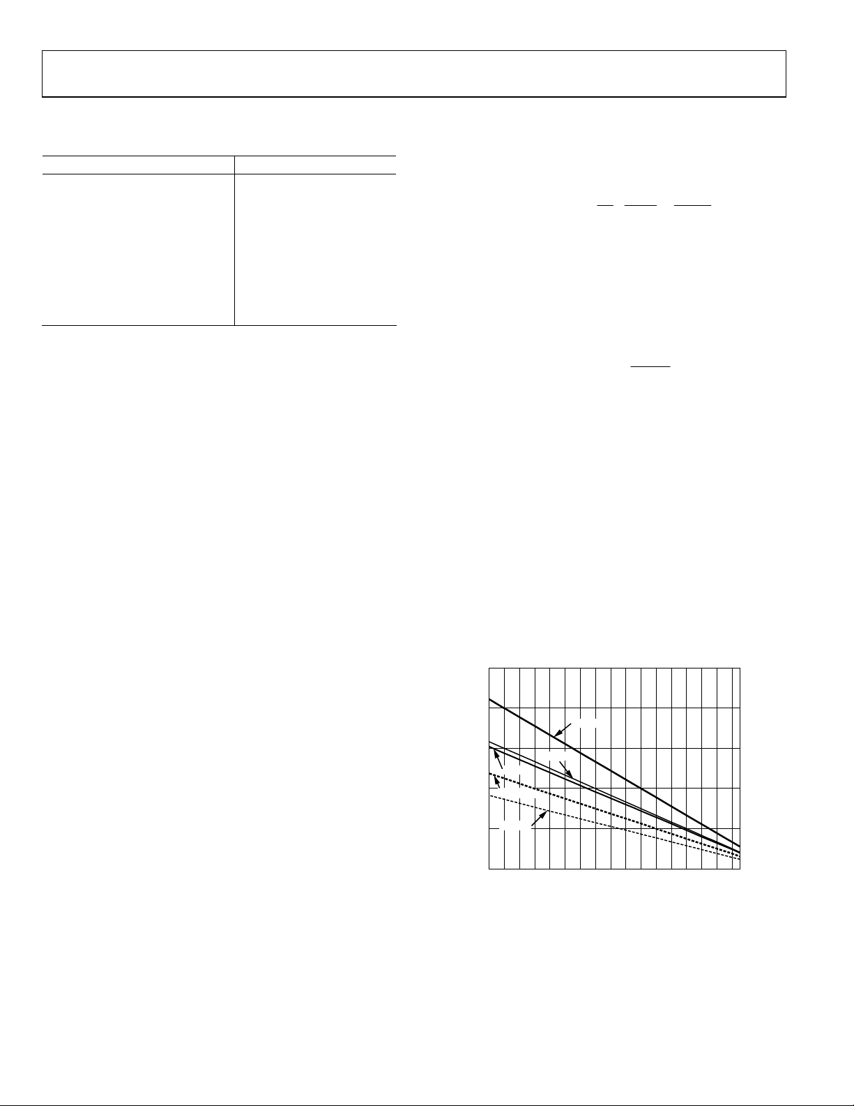
Figure 6 shows the maximum safe power dissipation in the
package versus the ambient temperature for the SOIC-8
(125°C/W), SOT23-8 (160°C/W), SOIC-14 (90°C/W),
TSSOP-14 (120°C/W), and SC70-6 (208°C/W) packages on a
JEDEC standard 4-layer board. θ
2.5
2.0
SOIC-14
1.5
1.0
0.5
MAXIMUM POWER DISSIPATION (W)
0
–40 –20–10–30 0 10 20 30 40 50 60 70 80 90 100110120
TSSOP-14
SOIC-8
SOT-23-8
SC70-6
AMBIENT TEMPERATURE (°C)
Figure 6. Maximum Power Dissipation
values are approximations.
JA
03679-A-018
Output Short Circuit
Shorting the output to ground or drawing excessive current
from the AD8029/AD8030/AD8040 could cause catastrophic
failure.
Rev. A | Page 6 of 20
 Loading...