ANALOG DEVICES AD8028 Service Manual

Low Distortion, High Speed
FEATURES
High speed
190 MHz, –3 dB bandwidth (G = +1)
100 V/μs slew rate
Low distortion
120 dBc @ 1 MHz SFDR
80 dBc @ 5 MHz SFDR
Selectable input crossover threshold
Low noise
4.3 nV/√Hz
1.6 pA/√Hz
Low offset voltage: 900 μV max
Low power: 6.5 mA/amplifier supply current
Power-down mode
No phase reversal: V
Wide supply range: 2.7 V to 12 V
Small packaging: SOIC-8, SOT-23-6, MSOP-10
APPLICATIONS
Filters
ADC drivers
Level shifting
Buffering
Professional video
Low voltage instrumentation
GENERAL DESCRIPTION
The AD8027/AD80281 are high speed amplifiers with rail-torail input and output that operate on low supply voltages and
are optimized for high performance and wide dynamic signal
range. The AD8027/AD8028 have low noise (4.3 nV/√Hz,
1.6 pA/√Hz) and low distortion (120 dBc at 1 MHz). In applications that use a fraction of, or the entire input dynamic range
and require low distortion, the AD8027/AD8028 are ideal
choices.
Many rail-to-rail input amplifiers have an input stage that
switches from one differential pair to another as the input signal
crosses a threshold voltage, which causes distortion. The
AD8027/AD8028 have a unique feature that allows the user to
select the input crossover threshold voltage through the
SELECT pin. This feature controls the voltage at which the
complementary transistor input pairs switch. The AD8027/
AD8028 also have intrinsically low crossover distortion.
> |VS| + 200 mV
IN
Rail-to-Rail Input/Output Amplifiers
AD8027/AD8028
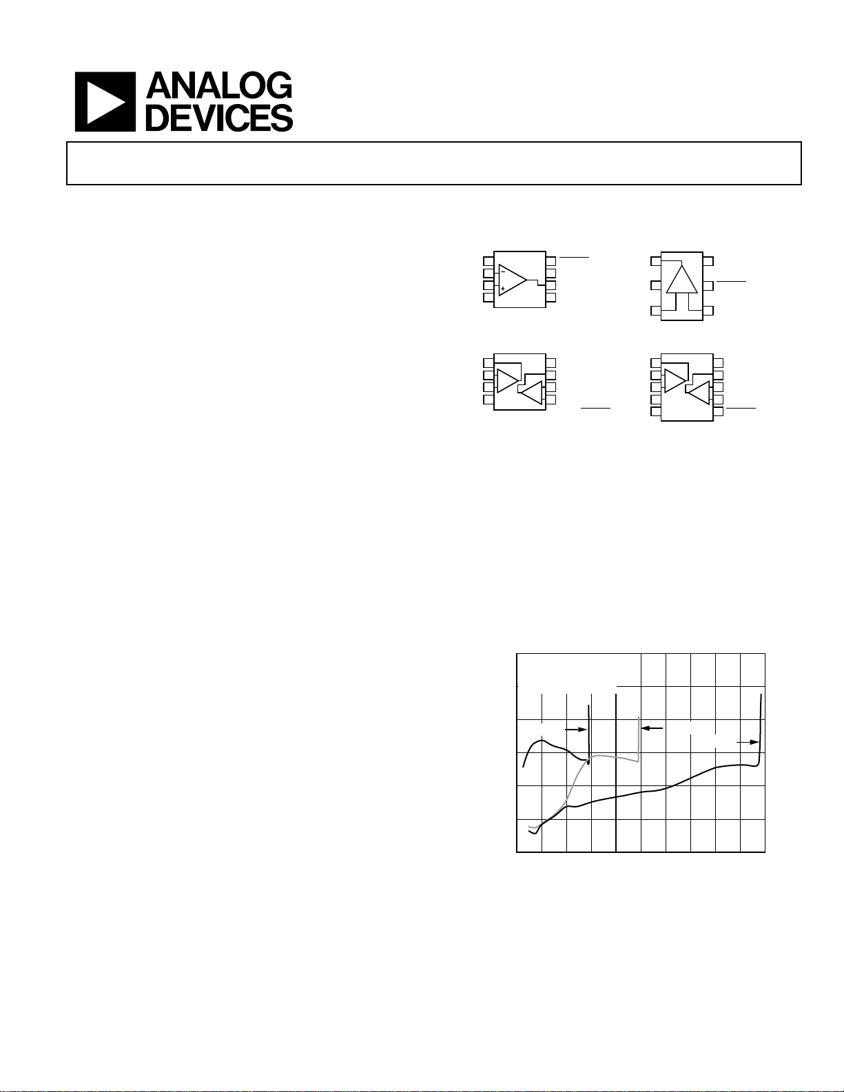
CONNECTION DIAGRAMS
V
–IN A
+IN A
V
OUT
–V
OUTA
–V
+IN
AD8027
SOT-23-6
(RT)
1
2
S
3
1
2
3
4
S
5
+–
AD8028
MSOP-10
(RM)
–
+
V
= +5V
S
03327-B-001
VS = ±5V
6
5
4
–
+
+V
S
DISABLE/SELECT
–IN
10
+V
S
9
V
OUTB
–IN B
8
7
+IN B
6
DISABLE/SELECT B
03327-A-063
0
AD8027
SOIC-8
(R)
NC
V
+IN
–V
OUTA
–IN A
+IN A
–V
–IN
S
S
1
2
3
4
NC = NO CONNECT
AD8028
SOIC-8
1
–
2
3
+
4
8
DISABLE/SELECT
+V
7
S
V
6
OUT
NC
5
(R)
8
+V
S
7
V
OUTB
–IN B
6
–
+
5
+IN B
DISABLE/SELECT A
Figure 1. Connection Diagrams (Top View)
With their wide supply voltage range (2.7 V to 12 V) and wide
bandwidth (190 MHz), the AD8027/AD8028 amplifiers are
designed to work in a variety of applications where speed and
performance are needed on low supply voltages. The high performance of the AD8027/AD8028 is achieved with a quiescent
current of only 6.5 mA/amplifier typical. The AD8027/AD8028
have a shutdown mode that is controlled via the SELECT pin.
The AD8027/AD8028 are available in SOIC-8, MSOP-10, and
SOT-23-6 packages. They are rated to work over the industrial
temperature range of –40°C to +125°C.
–20
G = +1
FREQUENCY = 100kHz
R
= 1kΩ
L
–40
–60
= +3V
V
S
–80
SFDR (dB)
–100
–120
–140
01234567891
1
Protected by U.S. patent numbers 6,486,737B1; 6,518,842B1
OUTPUT VOLTAGE (V p-p)
Figure 2. SFDR vs. Output Amplitude
Rev. C
Information furnished by Analog Devices is believed to be accurate and reliable.
However, no responsibility is assumed by Analog Devices for its use, nor for any
infringements of patents or other rights of third parties that may result from its use.
Specifications subject to change without notice. No license is granted by implication
or otherwise under any patent or patent rights of Analog Devices. Trademarks and
registered trademarks are the property of their respective owners.
One Technology Way, P.O. Box 9106, Norwood, MA 02062-9106, U.S.A.
Tel: 781.329.4700 www.analog.com
Fax: 781.461.3113 © 2005 Analog Devices, Inc. All rights reserved.

AD8027/AD8028
TABLE OF CONTENTS
Specifications..................................................................................... 3
Wideband Operation ..................................................................... 19
Absolute Maximum Ratings............................................................ 6
Maximum Power Dissipation ..................................................... 6
ESD Caution.................................................................................. 6
Typical Performance Characteristics .............................................8
Theory of Operation ...................................................................... 17
Input Stage................................................................................... 17
Crossover Selection.................................................................... 17
Output Stage................................................................................ 18
DC Errors.................................................................................... 18
REVISION HISTORY
3/05—Rev. B to Rev. C
Updated Format..................................................................Universal
Change to Figure 1 ........................................................................... 1
10/03—Rev. A to Rev. B
Changes to Figure 1...........................................................................1
Circuit Considerations .............................................................. 19
Applications..................................................................................... 21
Using the SELECT Pin............................................................... 21
Driving a 16-Bit ADC................................................................ 21
Band-Pass Filter.......................................................................... 22
Design Tools and Technical Support....................................... 22
Outline Dimensions .......................................................................23
Ordering Guide .......................................................................... 24
8/03—Rev. 0 to Rev. A
Addition of AD8028........................................................... Universal
Changes to GENERAL DESCRIPTION.........................................1
Changes to Figures 1, 3, 4, 8, 13, 15, 17......................... 1, 6, 7, 8, 9
Changes to Figures 58, 60........................................................ 18, 20
Changes to SPECIFICATIONS........................................................3
Updated OUTLINE DIMENSIONS .............................................22
Updated ORDERING GUIDE.......................................................23
3/03—Revision 0: Initial Version
Rev. C | Page 2 of 24

AD8027/AD8028
SPECIFICATIONS
VS = ±5 V at TA = 25°C, RL = 1 kΩ to midsupply, G = 1, unless otherwise noted.
Table 1.
Parameter Conditions Min Typ Max Unit
DYNAMIC PERFORMANCE
G = 1, VO = 2 V p-p 20 32 MHz
NOISE/DISTORTION PERFORMANCE
f
DC PERFORMANCE
T
T
INPUT CHARACTERISTICS
SELECT PIN
OUTPUT CHARACTERISTICS
POWER SUPPLY
1
No sign or a plus sign indicates current into the pin; a minus sign indicates current out of the pin.
–3 dB Bandwidth G = 1, VO = 0.2 V p-p 138 190 MHz
Bandwidth for 0.1 dB Flatness G = 2, VO = 0.2 V p-p 16 MHz
Slew Rate G = +1, VO = 2 V step/G = −1, VO = 2 V step 90/100 V/μs
Settling Time to 0.1% G = 2, VO = 2 V step 35 ns
Spurious-Free Dynamic Range (SFDR) fC = 1 MHz, VO = 2 V p-p, RF = 24.9 Ω 120 dBc
= 5 MHz, VO = 2 V p-p, RF = 24.9 Ω 80 dBc
C
Input Voltage Noise f = 100 kHz 4.3 nV/√Hz
Input Current Noise f = 100 kHz 1.6 pA/√Hz
Differential Gain Error NTSC, G = 2, R
Differential Phase Error NTSC, G = 2, R
= 150 Ω
L
= 150 Ω
L
Crosstalk, Output to Output G = 1, RL = 100 Ω, V
= ±5 V @ 1 MHz
V
S
= 2 V p-p,
OUT
0.1 %
0.2 Degrees
−93 dB
Input Offset Voltage SELECT = three-state or open, PNP active 200 800 μV
SELECT = high NPN active 240 900 μV
Input Offset Voltage Drift T
Input Bias Current
1
V
MIN
to T
MAX
1.50 μV/°C
VCM = 0 V, NPN active 4 6 μA
to T
MIN
MAX
= 0 V, PNP active −8 −11 μA
CM
to T
MIN
MAX
4 μA
−8 μA
Input Offset Current ±0.1 ±0.9 μA
Open-Loop Gain VO = ±2.5 V 100 110 dB
Input Impedance 6 MΩ
Input Capacitance 2 pF
Input Common-Mode Voltage Range −5.2 to +5.2 V
Common-Mode Rejection Ratio VCM = ±2.5 V 90 110 dB
Crossover Low, Selection Input Voltage Three-state < ±20 μA −3.3 to +5 V
Crossover High, Selection Input Voltage −3.9 to −3.3 V
Disable Input Voltage −5 to −3.9 V
Disable Switching Speed 50% of input to <10% of final V
O
980 ns
Enable Switching Speed 45 ns
Output Overdrive Recovery Time
VI = +6 V to −6 V, G = −1 40/45 ns
(Rising/Falling Edge)
Output Voltage Swing −VS + 0.10 +VS − 0.06,
+ 0.06
−V
S
+VS − 0.10 V
Short-Circuit Output Sinking and Sourcing 120 mA
Off Isolation VIN = 0.2 V p-p, f = 1 MHz, SELECT = low −49 dB
Capacitive Load Drive 30% overshoot 20 pF
Operating Range 2.7 12 V
Quiescent Current/Amplifier 6.5 8.5 mA
Quiescent Current (Disabled) SELECT = low 370 500 μA
Power Supply Rejection Ratio VS ± 1 V 90 110 dB
Rev. C | Page 3 of 24

AD8027/AD8028
VS = 5 V at TA = 25°C, RL = 1 kΩ to midsupply, unless otherwise noted.
Table 2.
Parameter Conditions Min Typ Max Unit
DYNAMIC PERFORMANCE
−3 dB Bandwidth G = 1, VO = 0.2 V p-p 131 185 MHz
G = 1, VO = 2 V p-p 18 28 MHz
Bandwidth for 0.1 dB Flatness G = 2, V
= 0.2 V p-p
O
Slew Rate G = +1, VO = 2 V step/G = −1, VO = 2 V step 85/100 V/μs
Settling Time to 0.1% G = 2, VO = 2 V step 40 ns
NOISE/DISTORTION PERFORMANCE
Spurious-Free Dynamic Range (SFDR) fC = 1 MHz, VO = 2 V p-p, RF = 24.9 Ω 90 dBc
f
= 5 MHz, VO = 2 V p-p, RF = 24.9 Ω 64 dBc
C
Input Voltage Noise f = 100 kHz 4.3 nV/√Hz
Input Current Noise f = 100 kHz 1.6 pA/√Hz
Differential Gain Error NTSC, G = 2, R
Differential Phase Error NTSC, G = 2, R
Crosstalk, Output to Output G = 1, RL = 100 Ω, V
= ±5 V @ 1 MHz
V
S
= 150 Ω
L
= 150 Ω
L
OUT
= 2 V p-p,
DC PERFORMANCE
Input Offset Voltage SELECT = three-state or open, PNP active 200 800 μV
SELECT = high NPN active 240 900 μV
Input Offset Voltage Drift T
Input Bias Current
1
T
V
T
to T
MIN
MAX
VCM = 2.5 V, NPN active 4 6 μA
to T
MIN
MAX
= 2.5 V, PNP active −8 −11 μA
CM
to T
MIN
MAX
Input Offset Current ±0.1 ±0.9 μA
Open-Loop Gain VO = 1 V to 4 V 96 105 dB
INPUT CHARACTERISTICS
Input Impedance 6 MΩ
Input Capacitance 2 pF
Input Common-Mode Voltage Range −0.2 to +5.2 V
Common-Mode Rejection Ratio VCM = 0 V to 2.5 V 90 105 dB
SELECT PIN
Crossover Low, Selection Input Voltage Three-state < ±20 μA 1.7 to 5 V
Crossover High, Selection Input Voltage 1.1 to 1.7 V
Disable Input Voltage 0 to 1.1 V
Disable Switching Speed 50% of input to <10% of final V
O
Enable Switching Speed 50 ns
OUTPUT CHARACTERISTICS
Overdrive Recovery Time
VI = −1 V to +6 V, G = −1 50/50 ns
(Rising/Falling Edge)
Output Voltage Swing RL = 1 kΩ −VS + 0.08 +VS − 0.04,
Off Isolation VIN = 0.2 V p-p, f = 1 MHz, SELECT = low −49 dB
Short-Circuit Current Sinking and sourcing 105 mA
Capacitive Load Drive 30% overshoot 20 pF
POWER SUPPLY
Operating Range 2.7 12 V
Quiescent Current/Amplifier 6 8.5 mA
Quiescent Current (Disabled) SELECT = low 320 450 μA
Power Supply Rejection Ratio VS ± 1 V 90 105 dB
1
No sign or a plus sign indicates current into the pin; a minus sign indicates current out of the pin.
12 MHz
0.1 %
0.2 Degrees
−92 dB
2 μV/°C
4 μA
−8 μA
1100 ns
+V
− 0.08 V
−V
+ 0.04
S
S
Rev. C | Page 4 of 24

AD8027/AD8028
VS = 3 V at TA = 25°C, RL = 1 kΩ to midsupply, unless otherwise noted.
Table 3.
Parameter Conditions Min Typ Max Unit
DYNAMIC PERFORMANCE
–3 dB Bandwidth G = 1, VO = 0.2 V p-p 125 180 MHz
G = 1, VO = 2 V p-p 19 29 MHz
Bandwidth for 0.1 dB Flatness G = 2, VO = 0.2 V p-p 10 MHz
Slew Rate G = +1, VO = 2 V step/G = –1, VO = 2 V step 73/100 V/μs
Settling Time to 0.1% G = 2, VO = 2 V step 48 ns
NOISE/DISTORTION PERFORMANCE
Spurious-Free Dynamic Range (SFDR) fC = 1 MHz, VO = 2 V p-p, RF = 24.9 Ω 85 dBc
f
Input Voltage Noise f = 100 kHz 4.3 nV/√Hz
Input Current Noise f = 100 kHz 1.6 pA/√Hz
Differential Gain Error NTSC, G = 2, R
Differential Phase Error NTSC, G = 2, R
Crosstalk, Output to Output G = 1, RL = 100 Ω, V
DC PERFORMANCE
Input Offset Voltage SELECT = three-state or open, PNP active 200 800 μV
SELECT = high NPN active 240 900 μV
Input Offset Voltage Drift T
Input Bias Current
1
T
V
T
Input Offset Current ±0.1 ±0.9 μA
Open-Loop Gain VO = 1 V to 2 V 90 100 dB
INPUT CHARACTERISTICS
Input Impedance 6 MΩ
Input Capacitance 2 pF
Input Common-Mode Voltage Range RL = 1 kΩ –0.2 to +3.2 V
Common-Mode Rejection Ratio VCM = 0 V to 1.5 V 88 100 dB
SELECT PIN
Crossover Low, Selection Input Voltage Three-state < ±20 μA 1.7 to 3 V
Crossover High, Selection Input Voltage 1.1 to 1.7 V
Disable Input Voltage 0 to 1.1 V
Disable Switching Speed 50% of input to <10% of final V
Enable Switching Speed 50 ns
OUTPUT CHARACTERISTICS
Output Overdrive Recovery Time
(Rising/Falling Edge)
Output Voltage Swing RL = 1 kΩ –VS + 0.07 +VS – 0.03,
Short-Circuit Current Sinking and sourcing 72 mA
Off Isolation VIN = 0.2 V p-p, f = 1 MHz, SELECT = low –49 dB
Capacitive Load Drive 30% Overshoot 20 pF
POWER SUPPLY
Operating Range 2.7 12 V
Quiescent Current/Amplifier 6.0 8.0 mA
Quiescent Current (Disabled) SELECT = low 300 420 μA
Power Supply Rejection Ratio VS ± 1 V 88 100 dB
1
No sign or a plus sign indicates current into the pin; a minus sign indicates current out of the pin.
= 5 MHz, VO = 2 V p-p, RF = 24.9 Ω 64 dBc
C
0.15 %
0.20 Degrees
–89 dB
2 μV/°C
= 3 V @ 1 MHz
V
S
to T
MIN
MAX
= 150 Ω
L
= 150 Ω
L
= 2 V p-p,
OUT
VCM = 1.5 V, NPN active 4 6 μA
to T
MIN
MAX
= 1.5 V, PNP active –8 –11 μA
CM
to T
MIN
MAX
O
V
= –1 V to +4 V, G = –1
I
4 μA
–8 μA
1150 ns
55/55 ns
+VS – 0.07 V
+ 0.03
–V
S
Rev. C | Page 5 of 24

AD8027/AD8028
(
)
(
ABSOLUTE MAXIMUM RATINGS
Table 4.
Parameter Rating
Supply Voltage 12.6 V
Power Dissipation See Figure 3
Common-Mode Input Voltage ±VS ± 0.5 V
Differential Input Voltage ±1.8 V
Storage Temperature –65°C to +125°C
Operating Temperature Range –40°C to +125°C
Lead Temperature Range
(Soldering 10 sec)
Junction Temperature 150°C
Stresses above those listed under Absolute Maximum Ratings
may cause permanent damage to the device. This is a stress
rating only; functional operation of the device at these or any
other conditions above those indicated in the operational
section of this specification is not implied. Exposure to absolute
maximum rating conditions for extended periods may affect
device reliability.
MAXIMUM POWER DISSIPATION
The maximum safe power dissipation in the AD8027/AD8028
package is limited by the associated rise in junction temperature
(T
) on the die. The plastic encapsulating the die locally reaches
J
the junction temperature. At approximately 150°C, which is the
glass transition temperature, the plastic changes its properties.
Even temporarily exceeding this temperature limit may change
the stresses that the package exerts on the die, permanently
shifting the parametric performance of the AD8027/AD8028.
Exceeding a junction temperature of 175°C for an extended
period of time can result in changes in the silicon devices,
potentially causing failure.
The still-air thermal properties of the package and PCB (θ
ambient temperature (T
package (P
) determine the junction temperature of the die.
D
The junction temperature can be calculated as
), and the total power dissipated in the
A
300°C
),
JA
The power dissipated in the package (P
) is the sum of the
D
quiescent power dissipation and the power dissipated in the
package due to the load drive for all outputs. The quiescent
power is the voltage between the supply pins (V
quiescent current (I
). Assuming the load (RL) is referenced to
S
midsupply, then the total drive power is V
which is dissipated in the package and some in the load (V
I
). The difference between the total drive power and the load
OUT
/2 × I
S
) times the
S
, some of
OUT
OUT
power is the drive power dissipated in the package.
= Quiescent Power + (Tota l Dri v e P o we r − Load Power)
P
D
⎛
V
()
D
⎜
IVP
SS
⎜
2
⎝
×+×=
⎞
V
OUTS
⎟
⎟
R
L
⎠
RMS output voltages should be considered. If R
, as in single-supply operation, then the total drive power
to V
S−
is V
× I
.
S
OUT
2
V
OUT
–
R
L
is referenced
L
If the rms signal levels are indeterminate, then consider the
worst case, when V
()
D
In single-supply operation with R
is V
= VS/2.
OUT
Airflow increases heat dissipation, effectively reducing θ
= VS/4 for RL to midsupply.
OUT
2
)
4/
V
S
+×=
IVP
SS
R
L
referenced to VS–, worst case
L
. Also,
JA
more metal directly in contact with the package leads from
metal traces, through holes, ground, and power planes reduces
the θ
. Care must be taken to minimize parasitic capacitances
JA
at the input leads of high speed op amps, as discussed in the
PCB Layout section.
×
θPTT ×+=
J
D
A
JA
ESD CAUTION
ESD (electrostatic discharge) sensitive device. Electrostatic charges as high as 4000 V readily accumulate on
the human body and test equipment and can discharge without detection. Although this product features
proprietary ESD protection circuitry, permanent damage may occur on devices subjected to high energy
electrostatic discharges. Therefore, proper ESD precautions are recommended to avoid performance degradation or loss of functionality.
Rev. C | Page 6 of 24

AD8027/AD8028
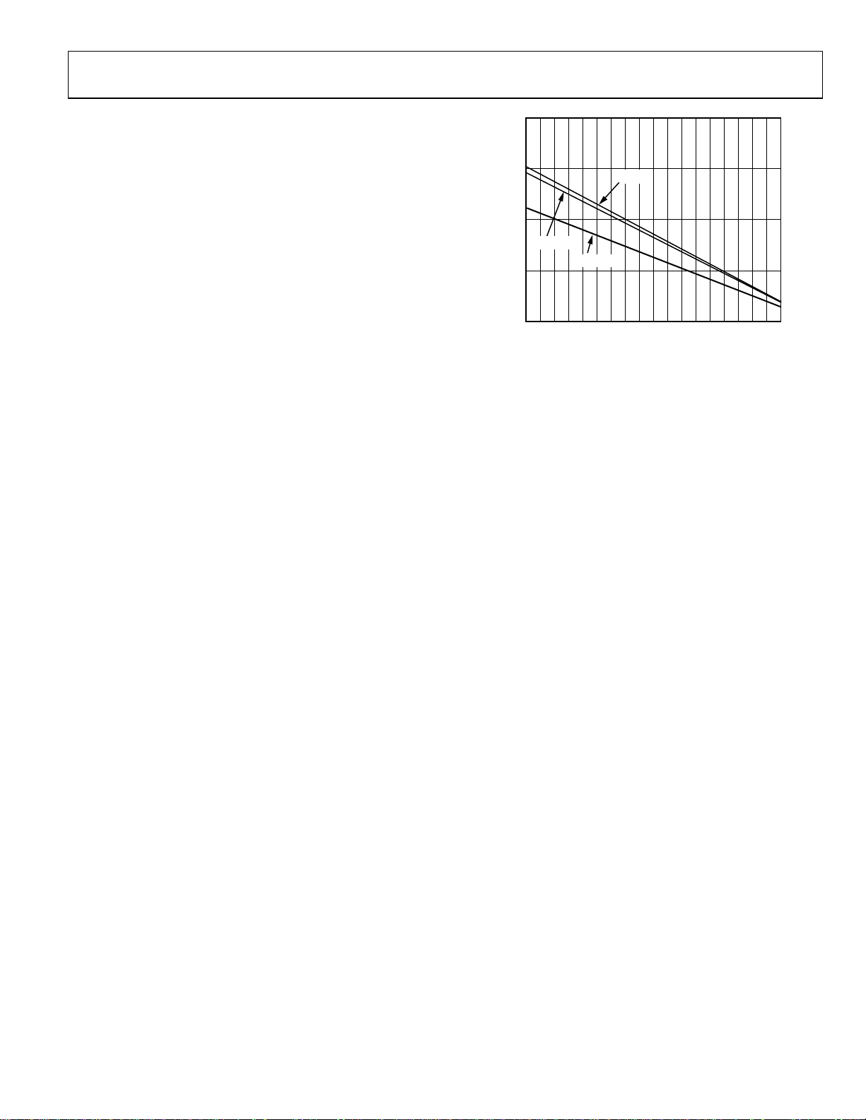
Figure 3 shows the maximum safe power dissipation in the
package vs. the ambient temperature for the SOIC-8
(125°C/W), SOT-23-6 (170°C/W), and MSOP-10 (130°C/W)
packages on a JEDEC standard 4-layer board.
Output Short Circuit
Shorting the output to ground or drawing excessive current
from the AD8027/AD8028 can likely cause catastrophic failure.
2.0
1.5
1.0
MSOP-10
0.5
MAXIMUM POWER DISSIPATION (W)
0
–55 –35 –15 5 25 45 65 85 105 125
SOT-23-6
SOIC-8
AMBIENT TEMPERATURE (°C)
03327-A-002
Figure 3. Maximum Power Dissipation vs. Ambient Temperature
Rev. C | Page 7 of 24

AD8027/AD8028
TYPICAL PERFORMANCE CHARACTERISTICS
Default conditions: VS = 5 V at TA = 25°C, RL = 1 kΩ, unless otherwise noted.
2
V
= 200mV p-p
OUT
1
0
–1
–2
–3
–4
–5
–6
–7
–8
NORMALIZED CLOSED-LOOP GAIN (dB)
–9
–10
0.1 1 10 100 1000
G = +10
G = –1
FREQUENCY (MHz)
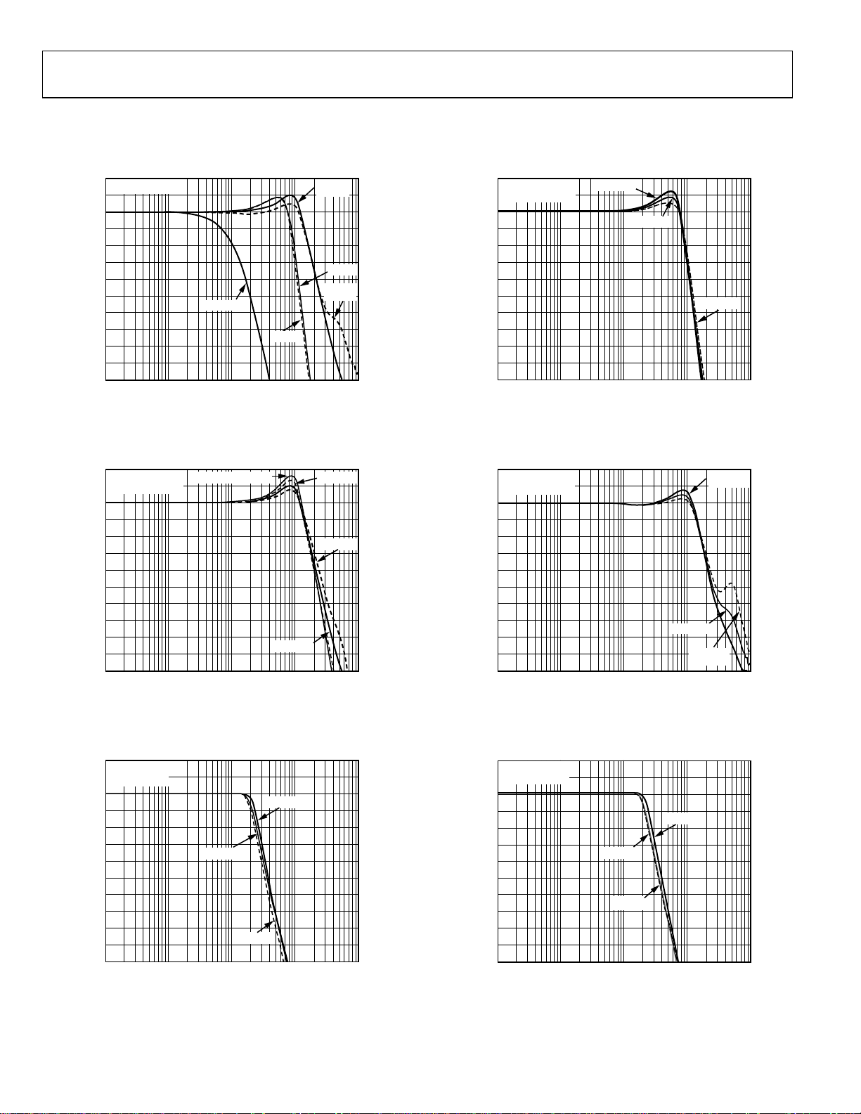
Figure 4. Small Signal Frequency Response for Various Gains
2
G = +1
1
V
= 200mV p-p
OUT
0
–1
–2
–3
–4
–5
–6
–7
CLOSED- LOOP GAIN (dB)
–8
–9
–10
0.1 1 10 100 1000
VS = +3V RF = 24.9Ω
VS = +5V
FREQUENCY (MHz)
Figure 5. AD8027 Small Signal Frequency Response for Various Supplies
2
G = +1
1
V
= 2V p-p
OUT
0
–1
–2
–3
–4
–5
–6
–7
CLOSED-LOOP GAIN (dB)
–8
–9
–10
0.1 1 10 1000
VS = +3V
FREQUENCY (MHz)
VS = ±5V
VS = +5V
Figure 6. Large Signal Frequency Response for Various Supplies
100
AD8027
G = +1
G = +2
AD8028
G = +1
03327-A-003
VS = +3V
VS = ±5V
03327-A-004
03327-A-005
8
G = +2
7
V
= 200mV p-p
OUT
6
5
4
3
2
1
0
–1
CLOSED-LOOP GAIN (dB)
–2
–3
–4
0.1 1 10 100 1000
VS = +3V
VS = +5V
FREQUENCY (MHz)
VS = ±5V
03327-A-006
Figure 7. Small Signal Frequency Response for Various Supplies
2
G = +1
1
V
= 200mV p-p
OUT
0
–1
–2
–3
–4
–5
–6
–7
CLOSED-LOOP GAIN (dB)
–8
–9
–10
0.1 1 10 100 1000
FREQUENCY (MHz)
V
S
= +5V
VS = ±5V
= +3V
V
S
03327-A-007
Figure 8. AD8028 Small Signal Frequency Response for Various Supplies
8
G = +2
7
= 2V p-p
V
OUT
6
5
4
3
2
1
0
–1
CLOSED-LOOP GAIN (dB)
–2
–3
–4
0.1 1 10 100 1000
VS = +5V
VS = +3V
FREQUENCY (MHz)
VS = ±5V
03327-A-008
Figure 9. Large Signal Frequency Response for Various Supplies
Rev. C | Page 8 of 24
 Loading...