Analog Devices AD8022 Datasheet

Dual High-Speed
FREQUENCY – Hz
3.0
10k
pA AND nV/ Hz
2.5
2.0
1.5
1.0
0.5
0
100k 1M
VOLTAGE NOISE, nV
CURRENT NOISE, pA
a
FEATURES
Low-Noise Amplifiers Provide Low Noise and Low
Distortion, Ideal for xDSL Modem Receiver
+5 V to ⴞ12 V Voltage Supply
Low-Power Consumption
4.0 mA/Amp (Typ) Supply Current
Voltage Feedback Amplifiers
Low Noise and Distortion
2.5 nV/√Hz Voltage Noise @ 100 kHz
SFDR –95 dBc @ 1 MHz
MTPR < –66 dBc
High Speed
120 MHz Bandwidth (–3 dB), G = 1
50 V/s Slew Rate
Low-Offset Voltage, 1.5 mV Typical
APPLICATIONS
ADSL, VDSL, HDSL, and Proprietary xDSL Systems
Low-Noise Instrumentation Front End
Ultrasound Preamp
Low-Noise Op Amps
AD8022
FUNCTIONAL BLOCK DIAGRAM
OUT1
–IN1
+IN1
–V
S
1
2
3
4
AD8022
–
+
8
+V
S
7
OUT2
6
–IN2
–
+
5
+IN2
PRODUCT DESCRIPTION
The AD8022 consists of two low-noise, high-speed, voltage feed-
back amplifiers. Both inputs add only 2.5 nV/√Hz of voltage
noise. These dual amplifiers provide wideband, low-distortion
performance, with high-output current optimized for stability
when driving capacitive loads. Operating from +5 V to ±12 V
supplies, the AD8022 typically consumes only 4.0 mA/Amp
quiescent current. The AD8022 is available in both an 8-lead
microSOIC and an 8-lead SOIC package. Fast overvoltage
recovery and wide bandwidth make the AD8022 ideal as the
receive channel front end to an ADSL, VDSL or proprietary
xDSL transceiver design.
Low-noise receive amplifiers in the AD8022 are independent
voltage feedback amplifiers and can be configured as the differential receiver from the line transformer or as independent active
filters in an xDSL line interface circuit.
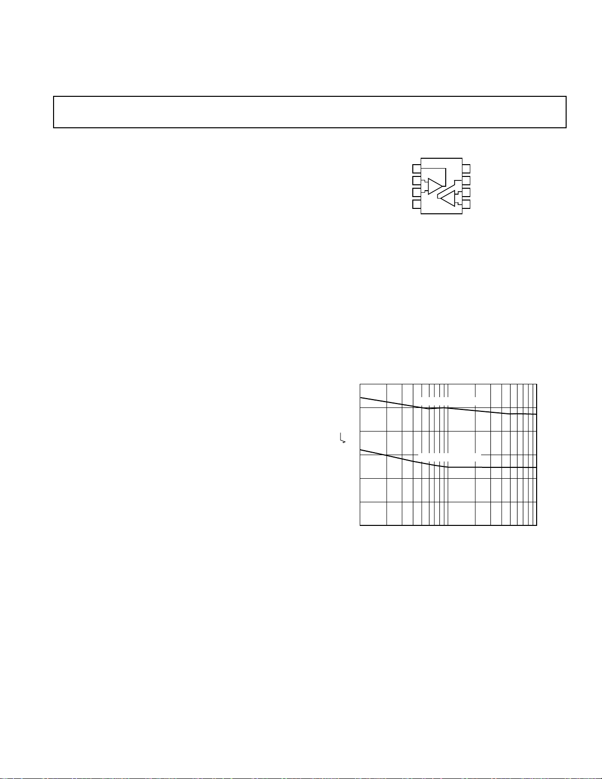
Figure 1. Current and Voltage Noise vs. Frequency
REV. 0
Information furnished by Analog Devices is believed to be accurate and
reliable. However, no responsibility is assumed by Analog Devices for its
use, nor for any infringements of patents or other rights of third parties
which may result from its use. No license is granted by implication or
otherwise under any patent or patent rights of Analog Devices.
One Technology Way, P.O. Box 9106, Norwood, MA 02062-9106, U.S.A.
Tel: 781/329-4700 World Wide Web Site: http://www.analog.com
Fax: 781/326-8703 © Analog Devices, Inc., 1999

AD8022–SPECIFICATIONS
(@ 25ⴗC, VS = ⴞ12 V, RL = 500 ⍀, G = 1, T
otherwise noted)
= –40ⴗC, T
MIN
= +85ⴗC, unless
MAX
Parameter Conditions Min Typ Max Unit
DYNAMIC PERFORMANCE
–3 dB Small Signal Bandwidth V
Bandwidth for 0.1 dB Flatness V
Large Signal Bandwidth V
Slew Rate V
Rise and Fall Time V
Settling Time 0.1% V
Overdrive Recovery Time V
= 0.2 V p-p 120 MHz
OUT
= 0.2 V p-p 25 MHz
OUT
= 4 V p-p 15 MHz
OUT
= 2 V p-p, G = 2 50 V/µs
OUT
= 2 V p-p, G = 2 30 ns
OUT
= 2 V p-p 62 ns
OUT
= 150% of Max Output
OUT
Voltage, G = 2 200 ns
NOISE/DISTORTION PERFORMANCE
Distortion V
Second Harmonic f
Third Harmonic f
Multitone Input Power Ratio
1
= 2 V p-p
OUT
= 1 MHz –95 dBc
C
= 1 MHz –100 dBc
C
G = 7 Differential
26 kHz to 132 kHz –67.2 dBc
144 kHz to 1.1 MHz –66 dBc
Voltage Noise (RTI) f = 100 kHz 2.5 nV/√Hz
Input Current Noise f = 100 kHz 1.2 pA/√Hz
INPUT CHARACTERISTICS
RTI Offset Voltage –6 –1.5 +6 mV
T
MIN
to T
MAX
–7.25 +7.25 mV
Input Bias Current –5 +2.5 +5 µA
to T
T
MIN
MAX
–7.5 +7.5 µA
Input Resistance (Differential) 20 kΩ
Input Capacitance 0.7 pF
Input Common-Mode Voltage Range –11.25 to +11.75 V
OUTPUT CHARACTERISTICS
Output Voltage Swing Single-Ended –10.1 +10.1 V
Short Circuit Output Current 100 mA
Capacitive Load Drive R
= 0 Ω, <3 dB of Peaking 75 pF
S
POWER SUPPLY
Operating Range +4.5 ±13.0 V
Quiescent Current 4.0 5.5 mA/Amp
T
Power Supply Rejection Ratio V
to T
MIN
S
MAX
= ±5 V to ±12 V 80 dB
6.1 mA
OPERATING TEMPERATURE RANGE –40 +85 °C
NOTES
1
Multitone testing performed with 800 mV rms across a 500 Ω load at Points A and B on Figure 17.
Specifications subject to change without notice.
–2–
REV. 0

SPECIFICATIONS
(@ 25ⴗC, VS = ⴞ2.5 V, RL = 500 ⍀, G = 1, T
otherwise noted)
= –40ⴗC, T
MIN
= +85ⴗC, unless
MAX
AD8022
Parameter Conditions Min Typ Max Unit
DYNAMIC PERFORMANCE
–3 dB Small Signal Bandwidth V
Bandwidth for 0.1 dB Flatness V
Large Signal Bandwidth V
Slew Rate V
Rise and Fall Time V
Settling Time 0.1% V
Overdrive Recovery Time V
= 0.2 V p-p 94 MHz
OUT
= 0.2 V p-p 22 MHz
OUT
= 3 V p-p 10 MHz
OUT
= 2 V p-p, G = 2 42 V/µs
OUT
= 2 V p-p, G = 2 40 ns
OUT
= 2 V p-p 75 ns
OUT
= 150% of Max Output
OUT
Voltage, G = 2 225 ns
NOISE/DISTORTION PERFORMANCE
Distortion V
Second Harmonic f
Third Harmonic f
Multitone Input Power Ratio
1
= 2 V p-p
OUT
= 1 MHz –77.5 dBc
C
= 1 MHz –94 dBc
C
G = 7 Differential, V
= ±6 V
S
26 kHz to 132 kHz –69 dBc
144 kHz to 1.1 MHz –66.7 dBc
Voltage Noise (RTI) f = 100 kHz 2.3 nV/√Hz
Input Current Noise f = 100 kHz 1 pA/√Hz
INPUT CHARACTERISTICS
RTI Offset Voltage –5.0 –0.8 +5.0 mV
T
MIN
to T
MAX
–6.25 +6.25 mV
Input Bias Current –5.0 +2.0 +5.0 µA
to T
T
MIN
MAX
7.5 µA
Input Resistance (Differential) 20 kΩ
Input Capacitance 0.7 pF
Input Common-Mode Voltage Range –1.83 to +2.5 V
OUTPUT CHARACTERISTICS
Output Voltage Swing Single-Ended –1.38 +1.48 V
Short Circuit Output Current 80 mA
Capacitive Load Drive R
= 0 Ω, <3 dB of Peaking 75 pF
S
POWER SUPPLY
Operating Range +4.5 ±13.0 V
Quiescent Current 3.5 4.25 mA/Amp
T
MIN
to T
MAX
4.4 mA
Power Supply Rejection Ratio ∆VS = ±1 V 86 dB
OPERATING TEMPERATURE RANGE –40 +85 °C
NOTES
1
Multitone testing performed with 800 mV rms across a 500 Ω load at Points A and B on Figure 17.
Specifications subject to change without notice.
REV. 0
–3–

AD8022
ABSOLUTE MAXIMUM RATINGS
Supply Voltage . . . . . . . . . . . . . . . . . . . . . . . . . . . . . . . . . 26 V
Internal Power Dissipation
2
1
Small Outline Package (R) . . . . . . . . . . . . . . . . . . . . . 1.6 W
microSOIC Package (RM) . . . . . . . . . . . . . . . . . . . . . 1.2 W
Input Voltage (Common Mode) . . . . . . . . . . . . . . . . . . . . ±V
S
Differential Input Voltage . . . . . . . . . . . . . . . . . . . . . . . ±0.8 V
Output Short Circuit Duration
. . . . . . . . . . . . . . . . . . . . . . Observe Power Derating Curves
Storage Temperature Range RM, R . . . . . . –65°C to +125°C
Operating Temperature Range (A Grade) . . . –40°C to +85°C
Lead Temperature Range (Soldering 10 sec) . . . . . . . . . 300°C
NOTES
1
Stresses above those listed under Absolute Maximum Ratings may cause perma-
nent damage to the device. This is a stress rating only; functional operation of the
device at these or any other conditions above those indicated in the operational
section of this specification is not implied. Exposure to absolute maximum rating
conditions for extended periods may affect device reliability.
2
Specification is for the device in free air:
8-Lead SOIC Package: θJA = 160°C/W.
8-Lead microSOIC Package: θJA = 200°C/W.
ORDERING GUIDE
Temperature Package Package
Model Range Description Option
AD8022AR –40°C to +85°C 8-Lead Plastic SOIC SO-8
AD8022ARM –40°C to +85°C 8-Lead microSOIC RM-8
AD8022AR-EVAL Evaluation Board SO-8
MAXIMUM POWER DISSIPATION
The maximum power that can be safely dissipated by the AD8022
is limited by the associated rise in junction temperature. The
maximum safe junction temperature for plastic encapsulated
devices is determined by the glass transition temperature of the
plastic, approximately 150°C. Temporarily exceeding this limit
may cause a shift in parametric performance due to a change
in the stresses exerted on the die by the package. Exceeding a
junction temperature of 175°C for an extended period can result
in device failure.
While the AD8022 is internally short circuit protected, this may not
be sufficient to guarantee that the maximum junction temperature
(150°C) is not exceeded under all conditions. To ensure proper
operation, it is necessary to observe the maximum power derating curves.
CAUTION
ESD (electrostatic discharge) sensitive device. Electrostatic charges as high as 4000 V readily
accumulate on the human body and test equipment and can discharge without detection. Although
the AD8022 features proprietary ESD protection circuitry, permanent damage may occur on
devices subjected to high-energy electrostatic discharges. Therefore, proper ESD precautions are
recommended to avoid performance degradation or loss of functionality.
2.0
1.5
8-LEAD SOIC PACKAGE
1.0
0.5
MAXIMUM POWER DISSIPATION – Watts
0
–50
8-LEAD MICROSOIC
–40 –30 –20 –10 0 10 20 30 40 50 60 70 80 90
AMBIENT TEMPERATURE – 8C
TJ = 150 8C
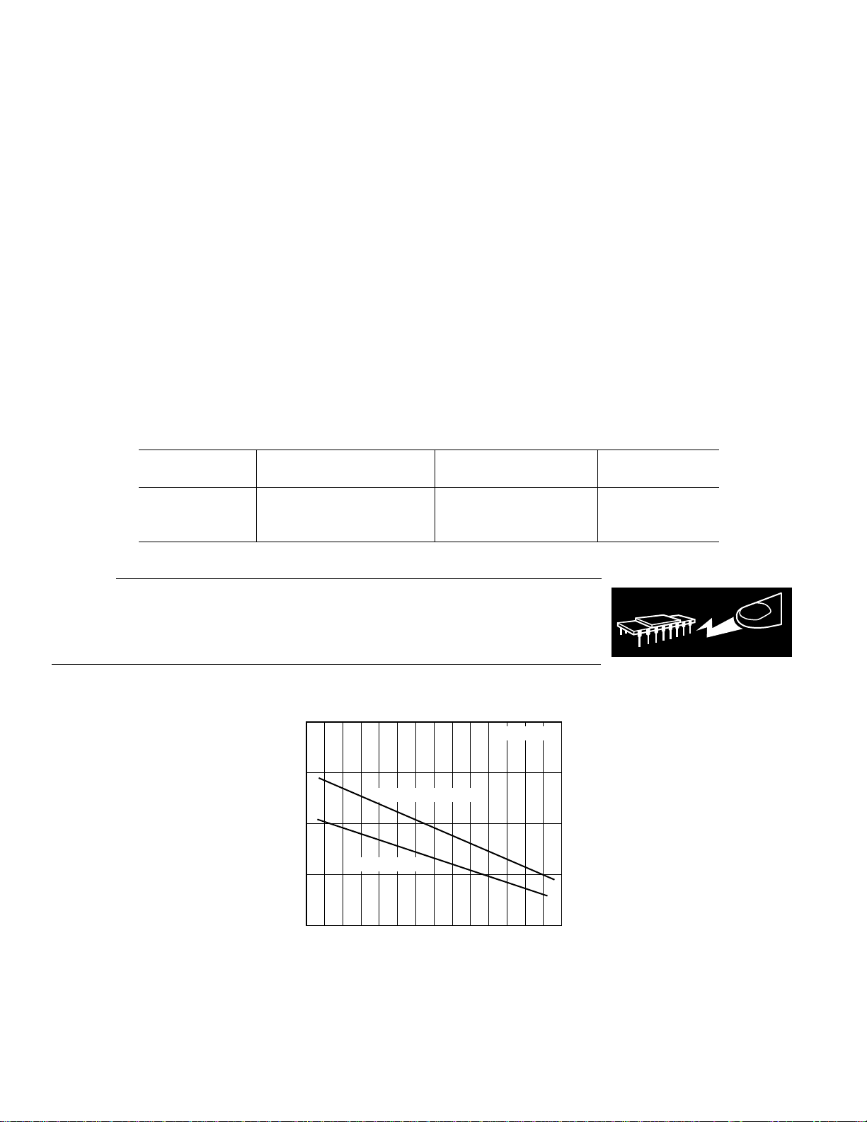
Figure 2. Plot of Maximum Power Dissipation vs.
Temperature
WARNING!
ESD SENSITIVE DEVICE
–4–
REV. 0

AD8022
FREQUENCY – MHz
dB
0.1 10 100 5001
5
4
3
2
1
0
–1
–2
–3
–4
–5
50V
50V
50V
R
F
+
RF = 402V
RF = 0V
RF = 715V
V
IN
V
OUT
FREQUENCY – Hz
0.4
100k
dB
0.3
0.2
0.1
0
–0.1
–0.2
–0.3
–0.4
–0.5
–0.6
1M 10M 100M
G = 2
RL = 509V
612V
65.0V
62.5V
SUPPLY VOLTAGE – Volts
70
2.5
SLEW RATE – V/ms
60
50
40
30
20
10
0
4.5 6.5 8.5 10.5 12.5
NEGATIVE EDGE
POSITIVE EDGE
dB
5
4
3
2
1
0
–1
–2
–3
–4
–5
0.1
V
50V
402V
V
453V
IN
+
VIN = 2V p-p
VIN = 0.8V p-p
1 10 100 500
OUT
56.2V
VIN = 0.4V p-p
FREQUENCY – MHz
VIN = 0.05V p-p
VIN = 0.2V p-p
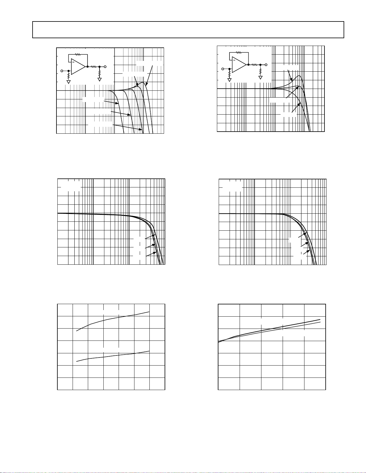
Figure 3. Frequency Response vs. Signal Level,
V
= ±12 V, G = 1
S
0.4
G = 1
0.3
RL = 509V
0.2
0.1
0
–0.1
dB
–0.2
–0.3
–0.4
–0.5
–0.6
100k
1M 10M 100M
FREQUENCY – Hz
612V
65.0V
62.5V
Figure 4. Fine-Scale Gain Flatness vs. Frequency, G = 1
Figure 6. Frequency Response vs. RF, G = 1, VS = ±12 V,
V
= 22 dBm
IN
Figure 7. Fine-Scale Gain Flatness vs. Frequency, G = 2
140
120
100
80
60
FREQUENCY – MHz
40
Figure 5. Bandwidth vs. Supply, RL = 500 Ω, VIN = –10 dBm
20
0
0142
REV. 0
G = +1, RF = 402V
G = +2, RF = 715V
4681012
SUPPLY VOLTAGE – 6Volts
Figure 8. Slew Rate vs. Supply Voltage, VS = ±12 V, G = 2
–5–
 Loading...