Analog Devices AD8007 8 d Datasheet
Ultralow Distortion
FREQUENCY – MHz
–30
–40
–110
1 10010
DISTORTION – dBc
–70
–80
–90
–100
–50
–60
THIRD
G = +2
R
L
= 150⍀
V
S
= 5V
V
OUT
= 2V p-p
SECOND
High Speed Amplifiers
AD8007/AD8008
FEATURES
Extremely Low Distortion
Second Harmonic
–88 dBc @ 5 MHz
–83 dBc @ 20 MHz (AD8007)
–77 dBc @ 20 MHz (AD8008)
Third Harmonic
–101 dBc @ 5 MHz
–92 dBc @ 20 MHz (AD8007)
–98 dBc @ 20 MHz (AD8008)
High Speed
650 MHz, –3 dB Bandwidth (G = +1)
1000 V/s Slew Rate
Low Noise
2.7 nV/
22.5 pA/
Hz Input Voltage Noise
√
Hz Input Inverting Current Noise
√
Low Power
9 mA/Amplifier Typ Supply Current
Wide Supply Voltage Range
5 V to 12 V
0.5 mV Typical Input Offset Voltage
Small Packaging
SOIC-8, MSOP, and SC70 Packages Available
APPLICATIONS
Instrumentation
IF and Baseband Amplifiers
Filters
A/D Drivers
DAC Buffers
GENERAL DESCRIPTION
The AD8007 (single) and AD8008 (dual) are high performance current feedback amplifiers with ultralow distortion
and noise. Unlike other high performance amplifiers, the low
price and low quiescent current allow these amplifiers to be
used in a wide range of applications. ADI’s proprietary second
generation eXtra-Fast Complementary Bipolar (XFCB)
process enables such high performance amplifiers with low
power consumption.
The AD8007/AD8008 have 650 MHz bandwidth, 2.7 nV/√Hz
voltage noise, –83 dB SFDR @ 20 MHz (AD8007), and –77 dBc
SFDR @ 20 MHz (AD8008).
With the wide supply voltage range (5 V to 12 V) and wide bandwidth, the AD8007/AD8008 are designed to work in a variety of
applications. The AD8007/AD8008 amplifiers have a low power
supply current of 9 mA/amplifier.
CONNECTION DIAGRAMS
SOIC (R) SC70 (KS-5)
AD8007
1
NC
(Top View)
2
–IN
3
+IN
–V
4
S
NC = NO CONNECT
8
NC
7
+V
6
V
5
NC
V
S
OUT
OUT
–V
+IN
S
AD8007
1
(Top View)
2
3
5
+V
S
4
–IN
SOIC (R) and MSOP (RM)
AD8008
(Top View)
1
V
OUT1
–IN1
27
36
+IN1
–V
45
S
8
+V
S
V
OUT2
–IN2
+IN2
The AD8007 is available in a tiny SC70 package as well as a
standard 8-lead SOIC. The dual AD8008 is available in both
8-lead SOIC and 8-lead MSOP packages. These amplifiers are
rated to work over the industrial temperature range of –40°C
to +85°C.
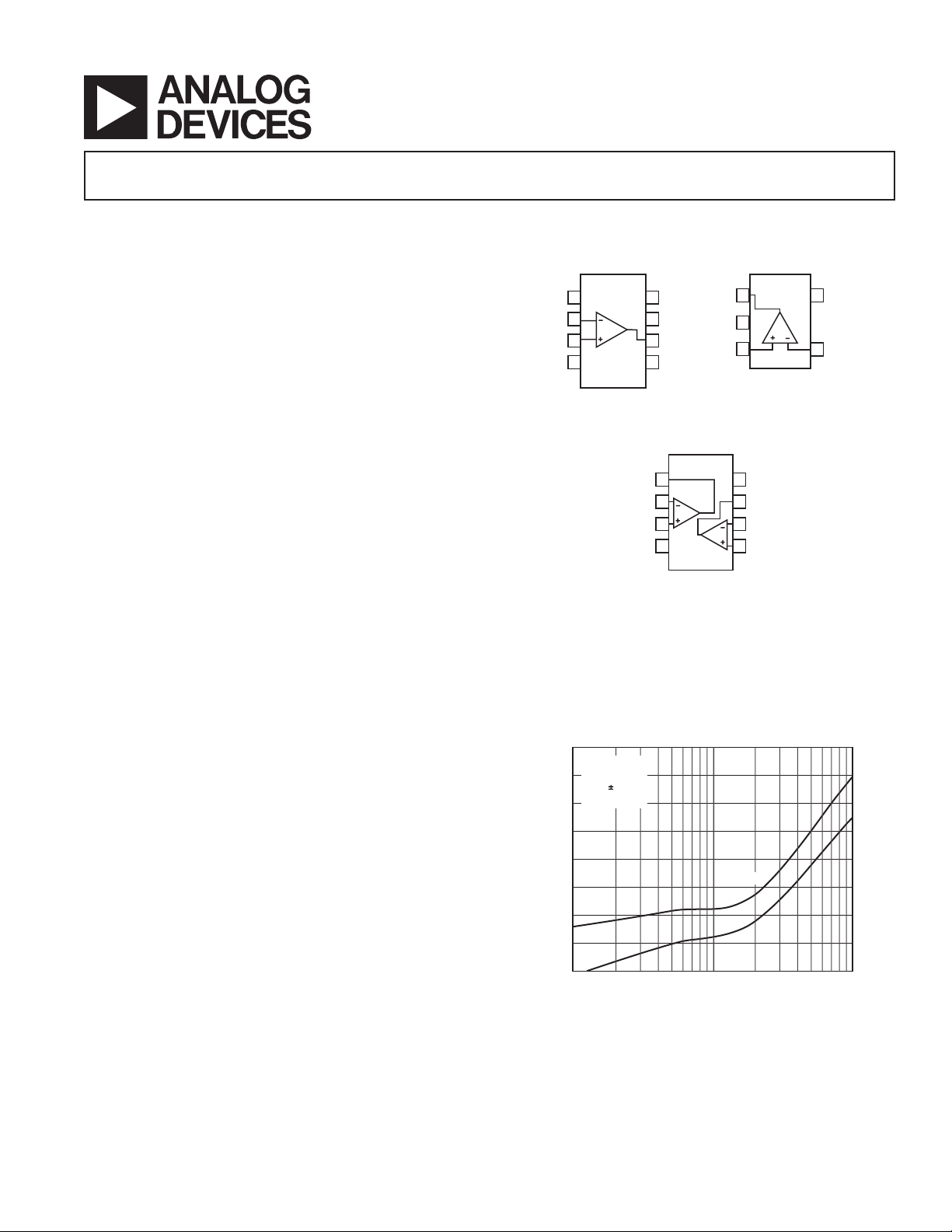
Figure 1. AD8007 Second and Third Harmonic
Distortion vs. Frequency
REV. D
Information furnished by Analog Devices is believed to be accurate and
reliable. However, no responsibility is assumed by Analog Devices for its
use, nor for any infringements of patents or other rights of third parties that
may result from its use. No license is granted by implication or otherwise
under any patent or patent rights of Analog Devices. Trademarks and
registered trademarks are the property of their respective companies.
One Technology Way, P.O. Box 9106, Norwood, MA 02062-9106, U.S.A.
Tel: 781/329-4700 www.analog.com
Fax: 781/326-8703 © 2003 Analog Devices, Inc. All rights reserved.

AD8007/AD8008–SPECIFICATIONS
VS = ⴞ5 V
Parameter Conditions Min Typ Max Unit
DYNAMIC PERFORMANCE
–3 dB Bandwidth G = +1, VO = 0.2 V p-p, RL = 1 kΩ 540 650 MHz
Bandwidth for 0.1 dB Flatness VO = 0.2 V p-p, G = +2, RL = 150 Ω 50 90 MHz
Overdrive Recovery Time ±2.5 V Input Step, G = +2, R
Slew Rate G = +1, V
Settling Time to 0.1% G = +2, VO = 2 V Step 18 ns
Settling Time to 0.01% G = +2, VO = 2 V Step 35 ns
NOISE/HARMONIC PERFORMANCE
Second Harmonic fC = 5 MHz, VO = 2 V p-p –88 dBc
Third Harmonic f
IMD f
Third Order Intercept f
Crosstalk (AD8008) f = 5 MHz, G = +2 –68 dB
Input Voltage Noise f = 100 kHz 2.7 nV/√Hz
Input Current Noise –Input, f = 100 kHz 22.5 pA/√Hz
Differential Gain Error NTSC, G = +2, R
Differential Phase Error NTSC, G = +2, RL = 150 Ω 0.010 Degree
DC PERFORMANCE
Input Offset Voltage 0.5 4 mV
Input Offset Voltage Drift 3 µV/°C
Input Bias Current +Input 4 8 µA
Input Bias Current Drift +Input 16 nA/°C
Transimpedance V
INPUT CHARACTERISTICS
Input Resistance +Input 4 MΩ
Input Capacitance +Input 1 pF
Input Common-Mode Voltage Range –3.9 to +3.9 V
Common-Mode Rejection Ratio VCM = ±2.5 V 56 59 dB
OUTPUT CHARACTERISTICS
Output Saturation Voltage VCC – VOH, VOL – VEE, RL = 1 kΩ 1.1 1.2 V
Short Circuit Current, Source 130 mA
Short Circuit Current, Sink 90 mA
Capacitive Load Drive 30% Overshoot 8 pF
POWER SUPPLY
Operating Range 5 12 V
Quiescent Current per Amplifier 9 10.2 mA
Power Supply Rejection Ratio
+PSRR 59 64 dB
–PSRR 59 65 dB
(@ TA = 25ⴗC, RS = 200 ⍀, RL = 150 ⍀, RF = 499 ⍀, Gain = +2, unless otherwise noted.)
AD8007/AD8008
G = +1, V
G = +2, V
G = +1, V
= 20 MHz, VO = 2 V p-p –83/–77 dBc
f
C
= 5 MHz, VO = 2 V p-p –101 dBc
C
= 20 MHz, VO = 2 V p-p –92/–98 dBc
f
C
= 19.5 MHz to 20.5 MHz, RL = 1 kΩ,
C
V
= 5 MHz, RL = 1 kΩ 43.0/42.5 dBm
C
= 20 MHz, RL = 1 kΩ 42.5 dBm
f
C
= 0.2 V p-p, RL = 150 Ω 250 500 MHz
O
= 0.2 V p-p, RL = 150 Ω 180 230 MHz
O
= 2 V p-p, RL = 1 kΩ 200 235 MHz
O
= 1 kΩ 30 ns
= 2 V Step 900 1000 V/µs
O
= 2 V p-p –77 dBc
O
L
+Input, f = 100 kHz 2 pA/√Hz
= 150 Ω 0.015 %
L
–Input 0.4 6 µA
–Input 9 nA/°C
= ±2.5 V, RL = 1 kΩ 1.0 1.5 MΩ
O
RL = 150 Ω 0.4 0.8 MΩ
REV. D–2–

AD8007/AD8008
VS = 5 V
(@ TA = 25ⴗC, RS = 200 ⍀, RL = 150 ⍀, RF = 499 ⍀, Gain = +2, unless otherwise noted.)
AD8007/AD8008
Parameter Conditions Min Typ Max Unit
DYNAMIC PERFORMANCE
–3 dB Bandwidth G = +1, V
= 0.2 V p-p, RL = 1 kΩ 520 580 MHz
O
G = +1, VO = 0.2 V p-p, RL = 150 Ω 350 490 MHz
G = +2, V
G = +1, V
= 0.2 V p-p, RL = 150 Ω 190 260 MHz
O
= 1 V p-p, RL = 1 kΩ 270 320 MHz
O
Bandwidth for 0.1 dB Flatness Vo = 0.2 V p-p, G = +2, RL = 150 Ω 72 120 MHz
Overdrive Recovery Time 2.5 V Input Step, G = +2, R
Slew Rate G = +1, V
= 2 V Step 665 740 V/µs
O
= 1 kΩ 30 ns
L
Settling Time to 0.1% G = +2, VO = 2 V Step 18 ns
Settling Time to 0.01% G = +2, VO = 2 V Step 35 ns
NOISE/HARMONIC PERFORMANCE
Second Harmonic f
Third Harmonic f
IMD f
Third Order Intercept f
= 5 MHz, VO = 1 V p-p –96/–95 dBc
C
f
= 20 MHz, VO = 1 V p-p –83/–80 dBc
C
= 5 MHz, VO = 1 V p-p –100 dBc
C
= 20 MHz, VO = 1 V p-p –85/–88 dBc
f
C
= 19.5 MHz to 20.5 MHz, RL = 1 kΩ, –89/–87 dBc
C
= 1 V p-p
V
O
= 5 MHz, RL = 1 kΩ 43.0 dBm
C
f
= 20 MHz, RL = 1 kΩ 42.5/41.5 dBm
C
Crosstalk (AD8008) Output to Output f = 5 MHz, G = +2 –68 dB
Input Voltage Noise f = 100 kHz 2.7 nV/√Hz
Input Current Noise –Input, f = 100 kHz 22.5 pA/√Hz
+Input, f = 100 kHz 2 pA/√Hz
DC PERFORMANCE
Input Offset Voltage 0.5 4 mV
Input Offset Voltage Drift 3 µV/°C
Input Bias Current +Input 4 8 µA
–Input 0.7 6 µA
Input Bias Current Drift +Input 15 nA/°C
–Input 8 nA/°C
Transimpedance V
= 1.5 V to 3.5 V, RL = 1 kΩ 0.5 1.3 MΩ
O
RL = 150 Ω 0.4 0.6 MΩ
INPUT CHARACTERISTICS
Input Resistance +Input 4 MΩ
Input Capacitance +Input 1 pF
Input Common-Mode Voltage Range 1.1 to 3.9 V
Common-Mode Rejection Ratio VCM = 1.75 V to 3.25 V 54 56 dB
OUTPUT CHARACTERISTICS
Output Saturation Voltage VCC – VOH, VOL – VEE, RL = 1 kΩ 1.05 1.15 V
Short Circuit Current, Source 70 mA
Short Circuit Current, Sink 50 mA
Capacitive Load Drive 30% Overshoot 8 pF
POWER SUPPLY
Operating Range 5 12 V
Quiescent Current per Amplifier 8.1 9 mA
Power Supply Rejection Ratio
+PSRR 59 62 dB
–PSRR 59 63 dB
REV. D
–3–
AD8007/AD8008
ABSOLUTE MAXIMUM RATINGS*
Supply Voltage . . . . . . . . . . . . . . . . . . . . . . . . . . . . . . . . 12.6 V
Power Dissipation . . . . . . . . . . . . . . . . . . . . . . . . See Figure 2
Common-Mode Input Voltage . . . . . . . . . . . . . . . . . . . . . ±V
S
Differential Input Voltage . . . . . . . . . . . . . . . . . . . . . . ± 1.0 V
Output Short Circuit Duration . . . . . . . . . . . . . . See Figure 2
Storage Temperature . . . . . . . . . . . . . . . . . . –65°C to +125°C
Operating Temperature Range . . . . . . . . . . . –40°C to +85°C
Lead Temperature Range (soldering 10 sec) . . . . . . . . . 300°C
*Stresses above those listed under Absolute Maximum Ratings may cause perma-
nent damage to the device. This is a stress rating only; functional operation of the
device at these or any other conditions above those indicated in the operational
section of this specification is not implied. Exposure to absolute maximum rating
conditions for extended periods may affect device reliability.
MAXIMUM POWER DISSIPATION
The maximum safe power dissipation in the AD8007/AD8008
packages is limited by the associated rise in junction temperature
) on the die. The plastic encapsulating the die will locally reach
(T
J
the junction temperature. At approximately 150°C, which is the
glass transition temperature, the plastic will change its properties. Even temporarily exceeding this temperature limit may
change the stresses that the package exerts on the die, permanently shifting the parametric performance of the AD8007/
AD8008. Exceeding a junction temperature of 175°C for an
extended period of time can result in changes in the silicon
devices, potentially causing failure.
The still-air thermal properties of the package and PCB (θ
ambient temperature (T
package (P
) determine the junction temperature of the die.
D
), and the total power dissipated in the
A
),
JA
The junction temperature can be calculated as follows:
TT P
=+ ×
ADA
JJ
θ
()
The power dissipated in the package (PD) is the sum of the quiescent power dissipation and the power dissipated in the package
due to the load drive for all outputs. The quiescent power is the
voltage between the supply pins (V
). Assuming the load (RL) is referenced to midsupply, the
(I
S
total drive power is V
/2 ⫻ I
S
package and some in the load (V
) times the quiescent current
S
, some of which is dissipated in the
OUT
OUT
⫻ I
). The difference
OUT
between the total drive power and the load power is the drive
power dissipated in the package.
P
= quiescent power + (total drive power – load power):
D
PVI
=×
()
DSS
+×
VVRV
S OUT
2
L
2
OUT
−
R
L
RMS output voltages should be considered. If RL is referenced
, as in single-supply operation, then the total drive power
to V
S
⫻ I
is V
S
OUT
.
If the rms signal levels are indeterminate, then consider the
worst case, when V
= VS/4 for RL to midsupply:
OUT
V
S
4
PVI
=×
()
DSS
+
R
L
2
In single-supply operation, with RL referenced to VS, worst case is
V
V
OUT
S
=
2
Airflow will increase heat dissipation, effectively reducing θJA.
Also, more metal directly in contact with the package leads from
metal traces, through holes, ground, and power planes will
reduce the θ
. Care must be taken to minimize parasitic capaci-
JA
tances at the input leads of high speed op amps as discussed in
the board layout section.
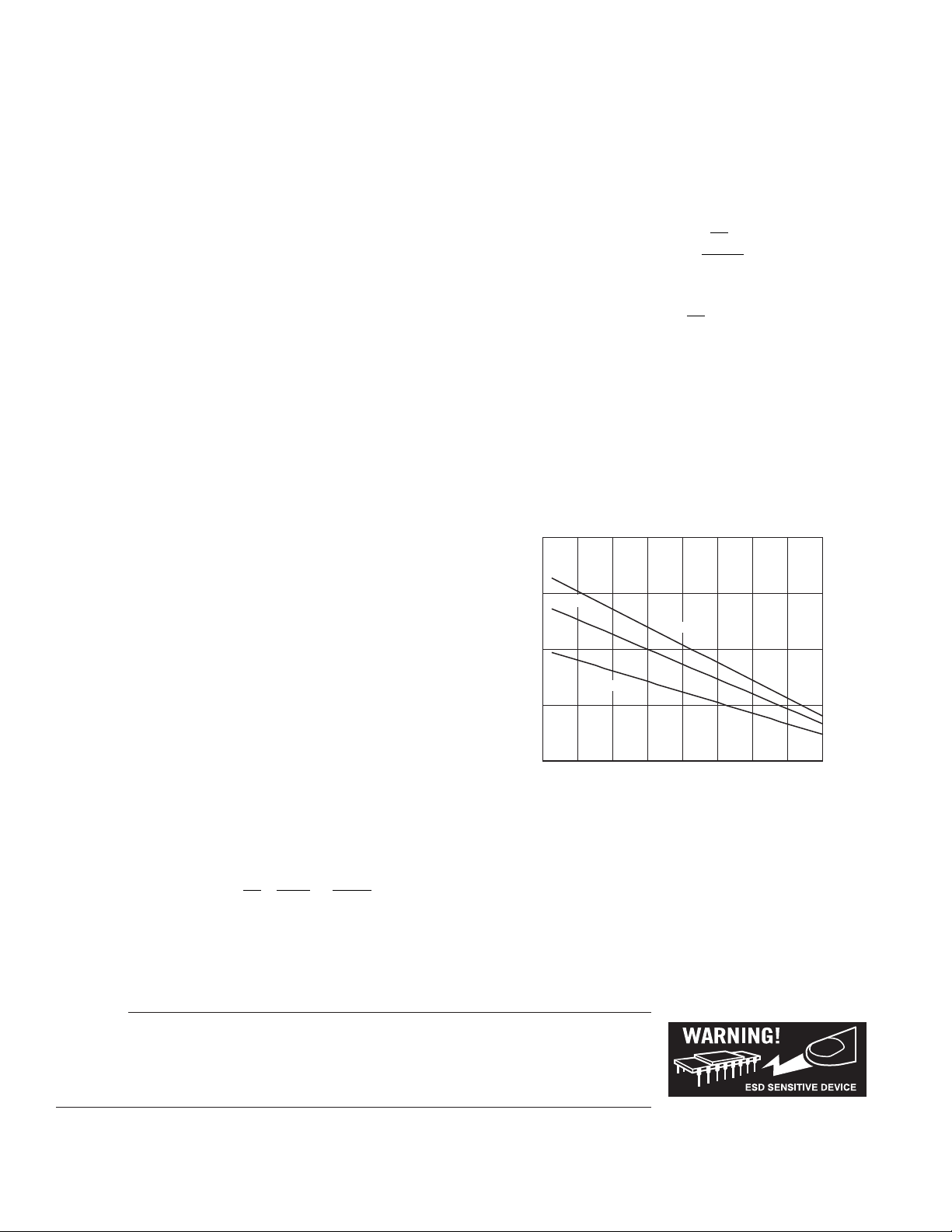
Figure 2 shows the maximum safe power dissipation in the package versus ambient temperature for the SOIC-8 (125°C/W),
MSOP (150°C/W), and SC70 (210°C/W) packages on a JEDEC
standard 4-layer board. θ
2.0
1.5
MSOP-8
1.0
0.5
MAXIMUM POWER DISSIPATION – W
0
–60 100–40
values are approximations.
JA
SOIC-8
SC70-5
–20 0 20 406080
AMBIENT TEMPERATURE – ⴗC
Figure 2. Maximum Power Dissipation vs.
Temperature for a 4-Layer Board
OUTPUT SHORT CIRCUIT
Shorting the output to ground or drawing excessive current for
the AD8007/AD8008 will likely cause catastrophic failure.
CAUTION
ESD (electrostatic discharge) sensitive device. Electrostatic charges as high as 4000 V readily
accumulate on the human body and test equipment and can discharge without detection. Although the
AD8007/AD8008 features proprietary ESD protection circuitry, permanent damage may occur on
devices subjected to high energy electrostatic discharges. Therefore, proper ESD precautions are
recommended to avoid performance degradation or loss of functionality.
REV. D–4–

AD8007/AD8008
ORDERING GUIDE
Package
Model Temperature Range Description Package Outline Branding
AD8007AR –40°C to +85°C 8-Lead SOIC R-8
AD8007AR-REEL –40°C to +85°C 8-Lead SOIC R-8
AD8007AR-REEL7 –40°C to +85°C 8-Lead SOIC R-8
AD8007AKS-R2 –40°C to +85°C 5-Lead SC70 KS-5 HTA
AD8007AKS-REEL –40°C to +85°C 5-Lead SC70 KS-5 HTA
AD8007AKS-REEL7 –40°C to +85°C 5-Lead SC70 KS-5 HTA
AD8008AR –40°C to +85°C 8-Lead SOIC R-8
AD8008AR-REEL7 –40°C to +85°C 8-Lead SOIC R-8
AD8008AR-REEL –40°C to +85°C 8-Lead SOIC R-8
AD8008ARM –40°C to +85°C 8-Lead MSOP RM-8 H2B
AD8008ARM-REEL –40°C to +85°C 8-Lead MSOP RM-8 H2B
AD8008ARM-REEL7 –40°C to +85°C 8-Lead MSOP RM-8 H2B
REV. D
–5–
AD8007/AD8008–Typical Performance Characteristics
(VS = ⴞ5 V, RL = 150 ⍀, RS = 200 ⍀, RF = 499 ⍀, unless otherwise noted.)
3
2
1
0
–1
–2
–3
–4
NORMALIZED GAIN – dB
–5
–6
–7
1 10010
G = +10
G = –1
FREQUENCY – MHz
G = +1
G = +2
1000
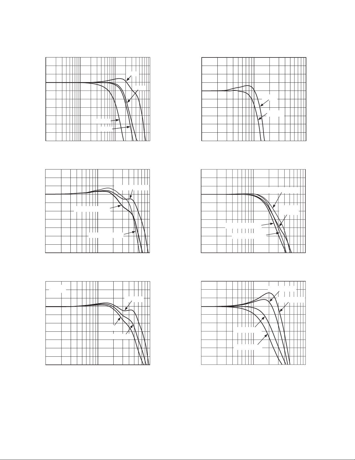
TPC 1. Small Signal Frequency Response for Various Gains
3
G = +1
2
1
0
–1
–2
GAIN – dB
–3
–4
–5
–6
–7
RL = 150⍀, VS = ⴞ5V
RL = 150⍀, VS = +5V
10010
FREQUENCY – MHz
RL = 1k⍀, VS = ⴞ5V
1000
6.4
G = +2
6.3
6.2
6.1
6.0
5.9
GAIN – dB
5.8
5.7
5.6
5.5
5.4
FREQUENCY – MHz
VS = +5V
VS = ⴞ5V
10010
TPC 4. 0.1 dB Gain Flatness; VS = +5, ±5 V
9
G = +2
8
7
6
5
4
GAIN – dB
3
2
1
0
–1
RL = 150⍀, VS = ⴞ5V
RL = 1k⍀, VS = ⴞ5V
FREQUENCY – MHz
10010
RL = 1k⍀, VS = +5V
RL = 150⍀
= +5V
V
S
1000
1000
TPC 2. Small Signal Frequency Response for VS and R
3
G = +1
2
= 1k⍀
R
L
1
0
–1
–2
GAIN – dB
–3
–4
–5
–6
–7
RS = 301⍀
10010
FREQUENCY – MHz
RS = 200⍀
RS = 249⍀
1000
TPC 3. Small Signal Frequency Response for
Various R
Values
S
LOAD
TPC 5. Small Signal Frequency Response for VS and R
9
G = +2
8
7
6
5
4
GAIN – dB
3
2
1
0
–1
RF = RG = 499⍀
RF = RG = 649⍀
10010
FREQUENCY – MHz
RF = RG = 324⍀
RF = RG = 249⍀
1000
TPC 6. Small Signal Frequency Response for Various
Feedback Resistors, R
F=RG
LOAD
REV. D–6–
 Loading...