4-Channel, 1.5 MSPS, 10-Bit and 12-Bit
V
www.BDTIC.com/ADI
FEATURES
Throughput rate: 1.5 MSPS
Specified for V
Low power
6 mW maximum at 1.5 MSPS with 3 V supplies
13.5 mW maximum at 1.5 MSPS with 5 V supplies
4 analog input channels with a sequencer
Software configurable analog inputs
4-channel single-ended inputs
2-channel fully differential inputs
2-channel pseudo differential inputs
Accurate on-chip 2.5 V reference
±0.2% maximum @ 25°C, 25 ppm/°C maximum (AD7934)
70 dB SINAD at 50 kHz input frequency
No pipeline delays
High speed parallel interface—word/byte modes
Full shutdown mode: 2 μA maximum
28-lead TSSOP package
of 2.7 V to 5.25 V
DD
Parallel ADCs with a Sequencer
AD7933/AD7934
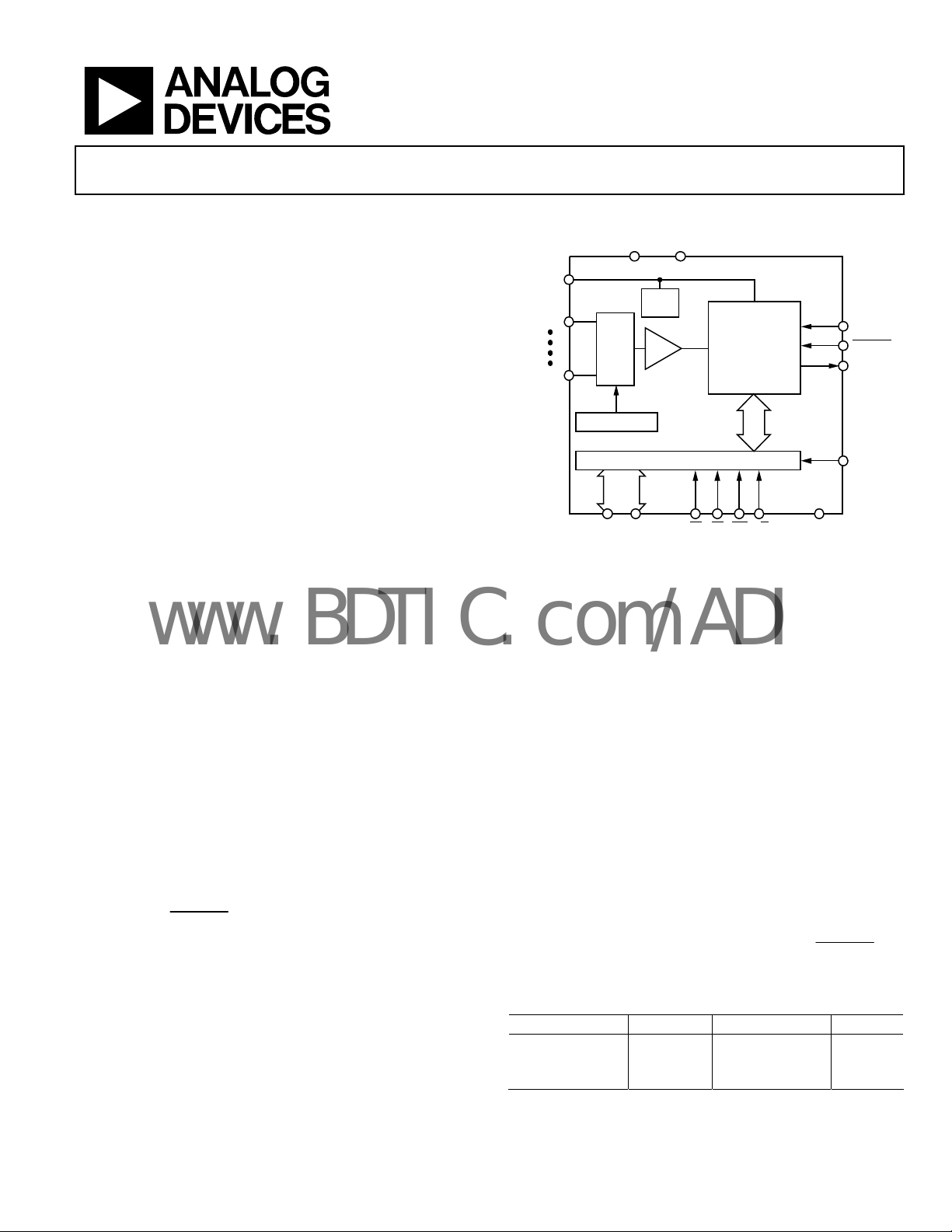
FUNCTIONAL BLOCK DIAGRAM
AGND
DD
V
V
REFOUT
REFIN/
VIN0
VIN3
2.5V
VREF
I/P
T/H
MUX
SEQUENCER
PARALLEL INTERFACE/CONTROL REGI STER
DB0 DB11
CS DGNDRD WR W/B
Figure 1.
AD7933/AD7934
12-/10-BIT
SAR ADC
AND
CONTROL
CLKIN
CONVST
BUSY
V
DRIVE
03713-001
GENERAL DESCRIPTION
The AD7933/AD7934 are 10-bit and 12-bit, high speed, low
power, successive approximation (SAR) analog-to-digital
converters (ADCs). The parts operate from a single 2.7 V to
5.25 V power supply and feature throughput rates up to 1.5 MSPS.
The parts contain a low noise, wide bandwidth, differential trackand-hold amplifier that handles input frequencies up to 50 MHz.
The AD7933/AD7934 feature four analog input channels with a
cha
nnel sequencer that allows a preprogrammed selection of
channels to be sequentially converted. These parts can accept
either single-ended, fully differential, or pseudo differential
analog inputs.
The conversion process and data acquisition are controlled
g standard control inputs that allow for easy interfacing to
usin
microprocessors and DSPs. The input signal is sampled on the
falling edge of
this point.
The AD7933/AD7934 has an accurate on-chip 2.5 V reference
t
hat is used as the reference source for the analog-to-digital
conversion. Alternatively, this pin can be overdriven to provide
an external reference.
CONVST
, and the conversion is also initiated at
These parts use advanced design techniques to achieve very low
p
ower dissipation at high throughput rates. They also feature
flexible power management options. An on-chip control
register allows the user to set up different operating conditions,
including analog input range and configuration, output coding,
power management, and channel sequencing.
PRODUCT HIGHLIGHTS
1. High throughput with low power consumption.
2. F
our analog inputs with a channel sequencer.
ccurate on-chip 2.5 V reference.
3. A
4. Sin
5. Sing
6. N
7. A
Table 1. Related Devices
Device No. of Bits No. of Channels Speed
AD7938/AD7939 12/10 8 1.5 MSPS
AD7938-6 12 8 625 kSPS
AD7934-6 12 4 625 kSPS
gle-ended, pseudo differential or fully differential
analog inputs that are software selectable.
le-supply operation with V
The V
function allows the parallel interface to connect
DRIVE
function.
DRIVE
directly to 3 V or 5 V processor systems independent of V
o pipeline delay.
ccurate control of the sampling instant via a
CONVST
input and once-off conversion control.
DD
.
Rev. B
Information furnished by Analog Devices is believed to be accurate and reliable. However, no
responsibility is assumed by Anal og Devices for its use, nor for any infringements of patents or ot her
rights of third parties that may result from its use. Specifications subject to change without notice. No
license is granted by implication or otherwise under any patent or patent rights of Analog Devices.
Trademarks and registered trademarks are the property of their respective owners.
One Technology Way, P.O. Box 9106, Norwood, MA 02062-9106, U.S.A.
Tel: 781.329.4700 www.analog.com
Fax: 781.461.3113 ©2005–2007 Analog Devices, Inc. All rights reserved.

AD7933/AD7934
www.BDTIC.com/ADI
TABLE OF CONTENTS
Features.............................................................................................. 1
Converter Operation.................................................................. 17
Functional Block Diagram .............................................................. 1
General Description ......................................................................... 1
Product Highlights ........................................................................... 1
Revision History ............................................................................... 2
Specifications..................................................................................... 3
AD7933 Specifications................................................................. 3
AD7934 Specifications................................................................. 5
Timing Specifications .................................................................. 7
Absolute Maximum Ratings............................................................ 8
ESD Caution.................................................................................. 8
Pin Configuration and Function Descriptions............................. 9
Typical Performance Characteristics ........................................... 11
Terminology .................................................................................... 13
Control Register.............................................................................. 15
Sequencer Operation ................................................................. 16
ADC Transfer Function............................................................. 17
Typical Connection Diagram ................................................... 18
Analog Input Structure.............................................................. 18
Analog Inputs ............................................................................. 19
Analog Input Selection.............................................................. 21
Reference ..................................................................................... 22
Parallel Interface......................................................................... 23
Power Modes of Operation....................................................... 26
Power vs. Throughput Rate....................................................... 27
Microprocessor Interfacing....................................................... 27
Application Hints ........................................................................... 29
Grounding and Layout.............................................................. 29
Evaluating the AD7933/AD7934 Performance...................... 29
Outline Dimensions....................................................................... 30
Ordering Guide .......................................................................... 30
Circuit Information........................................................................ 17
REVISION HISTORY
2/07—Rev. A to Rev B
Changes to Timing Specifications.................................................. 7
Changes to Figure 13...................................................................... 12
12/05—Rev. 0 to Rev. A
Replaced Figures.................................................................Universal
Changes to General Description .................................................... 1
Changes to Product Highlights....................................................... 1
Added Table 1.................................................................................... 1
Changes to Specifications Section.................................................. 3
Changes to Table 5............................................................................ 9
Changes to Terminology Section.................................................. 13
Changes to Control Register Section ........................................... 15
Changes to Circuit Information Section ..................................... 17
Changes to Application Hints Section......................................... 29
1/05—Revision 0: Initial Version
Rev. B | Page 2 of 32
AD7933/AD7934
www.BDTIC.com/ADI
SPECIFICATIONS
AD7933 SPECIFICATIONS
VDD = V
T
MAX
Table 2.
Parameter Value1 Unit Test Conditions/Comments
DYNAMIC PERFORMANCE fIN = 50 kHz sine wave
Signal-to-Noise + Distortion (SINAD)2 61 dB min Differential mode
60 dB min Single-ended mode
Total Harmonic Distortion (THD)2 −70 dB max
Peak Harmonic or Spurious Noise (SFDR)2 −72 dB max
Intermodulation Distortion (IMD)2 fa = 30 kHz, fb = 50 kHz
Channel-to-Channel Isolation −75 dB typ fIN= 50 kHz, f
Aperture Delay2 5 ns typ
Aperture Jitter2 72 ps typ
Full Power Bandwidth2 50 MHz typ @ 3 dB
10 MHz typ @ 0.1 dB
DC ACCURACY
Resolution 10 Bits
Integral Nonlinearity2 ±0.5 LSB max
Differential Nonlinearity2 ±0.5 LSB max Guaranteed no missed codes to 10 bits
Single-Ended and Pseudo Differential
Input
Fully Differential Input Twos complement output coding
ANALOG INPUT
Single-Ended Input Range 0 to V
0 to 2 × V
Pseudo Differential Input Range
Fully Differential Input Range3
DC Leakage Current4 ±1 μA max
Input Capacitance 45 pF typ When in track
10 pF typ When in hold
= 2.7 V to 5.25 V, internal/external V
DRIVE
1
, unless otherwise noted.
= 2.5 V, unless otherwise noted. f
REF
= 25.5 MHz, f
CLKIN
Second-Order Terms −86 dB typ
Third-Order Terms −90 dB typ
Straight binary output coding
Offset Error2 ±2 LSB max
Offset Error Match2 ±0.5 LSB max
Gain Error2 ±1.5 LSB max
Gain Error Match2 ±0.5 LSB max
Positive Gain Error2 ±1.5 LSB max
Positive Gain Error Match2 ±0.5 LSB max
Zero-Code Error2 ±2 LSB max
Zero-Code Error Match2 ±0.5 LSB max
Negative Gain Error2 ±1.5 LSB max
Negative Gain Error Match2 ±0.5 LSB max
V RANGE bit = 0
REF
V RANGE bit = 1
REF
V
0 to V
IN+
0 to 2 × V
V
−0.3 to +0.7 V typ VDD = 3 V
IN−
V RANGE bit = 0
REF
V RANGE bit = 1
REF
−0.3 to +1.8 V typ VDD = 5 V
V
V
IN+
IN+
and V
and V
V
IN−
V
IN−
± V
/2 V VCM = V
CM
REF
± V
V VCM = V
CM
REF
SAMPLE
= 300 kHz
NOISE
/2, RANGE bit = 0
REF
, RANGE bit = 1
REF
= 1.5 MSPS; TA = T
MIN
to
Rev. B | Page 3 of 32
AD7933/AD7934
www.BDTIC.com/ADI
Parameter Value
1
Unit Test Conditions/Comments
REFERENCE INPUT/OUTPUT
V
Input Voltage5 2.5 V ±1% specified performance
REF
DC Leakage Current
V
Output Voltage 2.5 V ±0.2% max @ 25°C
REFOUT
V
Temperature Coefficient 25 ppm/°C max
REFOUT
4
±1 μA max
5 ppm/°C typ
V
Noise 10 μV typ 0.1 Hz to 10 Hz bandwidth
REF
130 μV typ 0.1 Hz to 1 MHz bandwidth
V
Output Impedance 10 Ω typ
REF
V
Input Capacitance 15 pF typ When in track
REF
25 pF typ When in hold
LOGIC INPUTS
Input High Voltage, V
Input Low Voltage, V
Input Current, IIN ±5 μA max Typically 10 nA, VIN = 0 V or V
Input Capacitance, C
2.4 V min
INH
0.8 V max
INL
4
IN
10 pF max
DRIVE
LOGIC OUTPUTS
Output High Voltage, VOH 2.4 V min I
Output Low Voltage, VOL 0.4 V max I
SOURCE
= 200 μA
SINK
= 200 μA
Floating-State Leakage Current ±3 μA max
Floating-State Output Capacitance
4
10 pF max
Output Coding Straight (natural) binary CODING bit = 0
Twos complement CODING bit = 1
CONVERSION RATE
Conversion Time t2 + 13 t
ns
CLK
Track-and-Hold Acquisition Time 125 ns max Full-scale step input
80 ns typ Sine wave input
Throughput Rate 1.5 MSPS max
POWER REQUIREMENTS
VDD 2.7/5.25 V min/max
V
2.7/5.25 V min/max
DRIVE
6
I
DD
Digital inputs = 0 V or V
DRIVE
Normal Mode (Static) 0.8 mA typ VDD = 2.7 V to 5.25 V, SCLK on or off
Normal Mode (Operational) 2.7 mA max VDD = 4.75 V to 5.25 V
2.0 mA max VDD = 2.7 V to 3.6 V
Autostandby Mode 0.3 mA typ F
= 100 kSPS, VDD = 5 V
SAMPLE
160 μA typ Static
Full/Autoshutdown Mode (Static) 2 μA max SCLK on or off
Power Dissipation
Normal Mode (Operational) 13.5 mW max VDD = 5 V
6 mW max VDD = 3 V
Autostandby Mode (Static) 800 μW typ VDD = 5 V
480 μW typ VDD = 3 V
Full/Autoshutdown Mode 10 μW max VDD = 5 V
6 μW max VDD = 3 V
1
Temperature range is −40°C to +85°C.
2
See Terminology section.
3
VCM is the common-mode voltage. For full common-mode range, see Figure 25 and Figure 26. V
4
Sample tested during initial release to ensure compliance.
5
This device is operational with an external reference in the range of 0.1 V to VDD. See the Reference section for more information.
6
Measured with a midscale dc analog input.
IN+
and V
must always remain within GND/VDD.
IN−
Rev. B | Page 4 of 32
AD7933/AD7934
www.BDTIC.com/ADI
AD7934 SPECIFICATIONS
VDD = V
T
= T
A
= 2.7 V to 5.25 V, internal/external V
DRIVE
MIN
to T
, unless otherwise noted.
MAX
= 2.5 V, unless otherwise noted. f
REF
= 25.5 MHz, f
CLKIN
= 1.5 MSPS;
SAMPLE
Table 3.
Parameter Value
DYNAMIC PERFORMANCE fIN = 50 kHz sine wave
Signal-to-Noise + Distortion (SINAD)
2
68 dB min Single-ended mode
Signal-to-Noise Ratio (SNR)
2
69 dB min Single-ended mode
Total Harmonic Distortion (THD)
2
−70 dB max −80 dB typ, single-ended mode
Peak Harmonic or Spurious Noise (SFDR)
Intermodulation Distortion (IMD)
2
2
Second-Order Terms −86 dB typ
Third-Order Terms −90 dB typ
Channel-to-Channel Isolation −85 dB typ fIN = 50 kHz, f
Aperture Delay
Aperture Jitter
Full Power Bandwidth
2
2
2
10 MHz typ @ 0.1 dB
DC ACCURACY
Resolution 12 Bits
Integral Nonlinearity
2
±1.5 LSB max Single-ended mode
Differential Nonlinearity
2
Differential Mode ±0.95 LSB max Guaranteed no missed codes to 12 bits
Single-Ended Mode −0.95/+1.5 LSB max Guaranteed no missed codes to 12 bits
Single-Ended and Pseudo Differential Input Straight binary output coding
Offset Error
Offset Error Match
Gain Error
Gain Error Match
2
2
2
2
Fully Differential Input
Positive Gain Error
Positive Gain Error Match
Zero-Code Error
Zero-Code Error Match
Negative Gain Error
Negative Gain Error Match
2
2
2
2
2
2
ANALOG INPUT
Single-Ended Input Range 0 to V
0 to 2 × V
Pseudo Differential Input Range
V
0 to V
IN+
0 to 2 × V
V
−0.3 to +0.7 V typ VDD = 3 V
IN−
−0.3 to +1.8 V typ VDD = 5 V
Fully Differential Input Range
V
and V
IN+
V
IN+
DC Leakage Current
V
IN−
and V
V
IN−
4
3
Input Capacitance 45 pF typ When in track
10 pF typ When in hold
1
Unit Test Conditions/Comments
70 dB min Differential mode
71 dB min Differential mode
−73 dB max −85 dB typ, differential mode
−73 dB max −82 dB typ
fa = 30 kHz, fb = 50 kHz
= 300 kHz
NOISE
5 ns typ
72 ps typ
50 MHz typ @ 3 dB
±1 LSB max Differential mode
±6 LSB max
±1 LSB max
±3 LSB max
±1 LSB max Twos complement output coding
±3 LSB max
±1 LSB max
±6 LSB max
±1 LSB max
±3 LSB max
±1 LSB max
V RANGE bit = 0
REF
V RANGE bit = 1
REF
V RANGE bit = 0
REF
V RANGE bit = 1
REF
± V
/2 V VCM = V
CM
REF
± V
V VCM = V
CM
REF
/2, RANGE bit = 0
REF
, RANGE bit = 1
REF
±1 μA max
Rev. B | Page 5 of 32
AD7933/AD7934
www.BDTIC.com/ADI
Parameter Value
1
Unit Test Conditions/Comments
REFERENCE INPUT/OUTPUT
V
Input Voltage5 2.5 V ±1% specified performance
REF
DC Leakage Current ±1 μA max
V
Output Voltage 2.5 V ±0.2% max @ 25°C
REFOUT
V
Temperature Coefficient 25 ppm/°C max
REFOUT
5 ppm/°C typ
V
Noise 10 μV typ 0.1 Hz to 10 Hz bandwidth
REF
130 μV typ 0.1 Hz to 1 MHz bandwidth
V
Output Impedance 10 Ω typ
REF
V
Input Capacitance 15 pF typ When in track-and-hold
REF
25 pF typ When in track-and-hold
LOGIC INPUTS
Input High Voltage, V
Input Low Voltage, V
Input Current, IIN ±5 μA max Typically 10 nA, VIN = 0 V or V
Input Capacitance, C
2.4 V min
INH
0.8 V max
INL
4
IN
10 pF max
DRIVE
LOGIC OUTPUTS
Output High Voltage, VOH 2.4 V min I
Output Low Voltage, VOL 0.4 V max I
SOURCE
= 200 μA
SINK
= 200 μA
Floating-State Leakage Current ±3 μA max
Floating-State Output Capacitance
4
10 pF max
Output Coding Straight (natural) binary CODING bit = 0
Twos complement CODING bit = 1
CONVERSION RATE
Conversion Time t2 + 13 t
ns
CLK
Track-and-Hold Acquisition Time 125 ns max Full-scale step input
80 ns typ Sine wave input
Throughput Rate 1.5 MSPS max
POWER REQUIREMENTS
VDD 2.7/5.25 V min/max
V
2.7/5.25 V min/max
DRIVE
6
I
DD
Digital inputs = 0 V or V
DRIVE
Normal Mode (Static) 0.8 mA typ VDD = 2.7 V to 5.25 V, SCLK on or off
Normal Mode (Operational) 2.7 mA max VDD = 4.75 V to 5.25 V
2.0 mA max VDD = 2.7 V to 3.6 V
Autostandby Mode 0.3 mA typ f
= 100 kSPS, VDD = 5 V
SAMPLE
160 μA typ Static
Full/Autoshutdown Mode (Static) 2 μA max SCLK on or off
Power Dissipation
Normal Mode (Operational) 13.5 mW max VDD = 5 V
6 mW max VDD = 3 V
Autostandby Mode (Static) 800 μW typ VDD = 5 V
480 μW typ VDD = 3 V
Full/Autoshutdown Mode 10 μW max VDD = 5 V
6 μW max VDD = 3 V
1
Temperature range is −40°C to +85°C.
2
See the Terminology section.
3
VCM is the common-mode voltage. For full common-mode range, see Figure 25 and Figure 26. V
4
Sample tested during initial release to ensure compliance.
5
This device is operational with an external reference in the range of 0.1 V to VDD. See the Reference section for more information.
6
Measured with a midscale dc analog input.
IN+
and V
must always remain within GND/VDD.
IN−
Rev. B | Page 6 of 32

AD7933/AD7934
www.BDTIC.com/ADI
TIMING SPECIFICATIONS
VDD = V
T
= T
A
Table 4.
Limit at T
Parameter1 AD7933 AD7934 Unit Description
2
f
CLKIN
25.5 25.5 MHz max
t
30 30 ns min
QUIET
t1 10 10 ns min
t2 15 15 ns min
t3 50 50 ns max CLKIN falling edge to BUSY rising edge
t4 0 0 ns min
t5 0 0 ns min
t6 10 10 ns min
t7 10 10 ns min
t8 10 10 ns min
t9 10 10 ns min New data valid before falling edge of BUSY
t10 0 0 ns min
t11 0 0 ns min
t12 30 30 ns min
3
t
13
4
t
14
50 50 ns max
t15 0 0 ns min
t16 0 0 ns min
t17 10 10 ns min Minimum time between reads/writes
t18 0 0 ns min
t19 10 10 ns min
t20 40 40 ns max CLKIN falling edge to BUSY falling edge
t21 15.7 15.7 ns min CLKIN low pulse width
t22 7.8 7.8 ns min CLKIN high pulse width
1
Sample tested during initial release to ensure compliance. All input signals are specified with t
1.6 V. All timing specifications are with a 25 pF load capacitance (see Figure 34, Figure 35, Figure 36, and Figure 37).
2
Minimum CLKIN for specified performance; with slower SCLK frequencies, performance specifications apply typically.
3
The time required for the output to cross 0.4 V or 2.4 V.
4
t14 is derived from the measured time taken by the data outputs to change 0.5 V. The measured number is then extrapolated back to remove the effects of charging or
discharging the 25 pF capacitor. This means that the time, t
bus loading.
= 2.7 V to 5.25 V, internal/external V
DRIVE
MIN
to T
, unless otherwise noted.
MAX
, T
MIN
MAX
700 700 kHz min CLKIN frequency
30 30 ns max
3 3 ns min
= 2.5 V, unless otherwise noted. f
REF
= 25.5 MHz, f
CLKIN
= 1.5 MSPS;
SAMPLE
Minimum time between end of read and start of next conversion, that is, the time from
when the da
CONVST
CONVST
to WR setup time
CS
to WR hold time
CS
pulse width
WR
ta bus goes into three-state until the next falling edge of CONVST
pulse width
falling edge to CLKIN falling edge setup time
Data setup time before WR
Data hold after WR
to RD setup time
CS
to RD hold time
CS
pulse width
RD
Data access time after RD
Bus relinquish time after RD
Bus relinquish time after RD
HBEN to RD
HBEN to RD
HBEN to WR
HBEN to WR
, quoted in the timing characteristics is the true bus relinquish time of the part and is independent of the
14
setup time
hold time
setup time
hold time
= t
= 5 ns (10% to 90% of VDD) and timed from a voltage level of
RISE
FALL
Rev. B | Page 7 of 32
AD7933/AD7934
www.BDTIC.com/ADI
ABSOLUTE MAXIMUM RATINGS
TA = 25°C, unless otherwise noted.
Table 5.
Parameter Rating
VDD to AGND/DGND −0.3 V to +7 V
V
to AGND/DGND −0.3 V to VDD + 0.3 V
DRIVE
Analog Input Voltage to AGND −0.3 V to VDD + 0.3 V
Digital Input Voltage to DGND −0.3 V to +7 V
V
to VDD −0.3 V to VDD + 0.3 V
DRIVE
Digital Output Voltage to AGND −0.3 V to V
V
to AGND −0.3 V to VDD + 0.3 V
REFIN
AGND to DGND −0.3 V to +0.3 V
Input Current to Any Pin Except Supplies1±10 mA
Operating Temperature Range
Commercial (B Version) −40°C to +85°C
Storage Temperature Range −65°C to +150°C
Junction Temperature 150°C
θJA Thermal Impedance (TSSOP) 97.9°C/W
θJC Thermal Impedance (TSSOP) 14°C/W
Lead Temperature, Soldering
Reflow Temperature (10 sec to 30 sec) 255°C
ESD 1.5 kV
1
Transient currents of up to 100 mA do not cause SCR latch-up.
DRIVE
+ 0.3 V
Stresses above those listed under Absolute Maximum Ratings
may cause permanent damage to the device. This is a stress
rating only; functional operation of the device at these or any
other conditions above those indicated in the operational
section of this specification is not implied. Exposure to absolute
maximum rating conditions for extended periods may affect
device reliability.
ESD CAUTION
Rev. B | Page 8 of 32
AD7933/AD7934
T
www.BDTIC.com/ADI
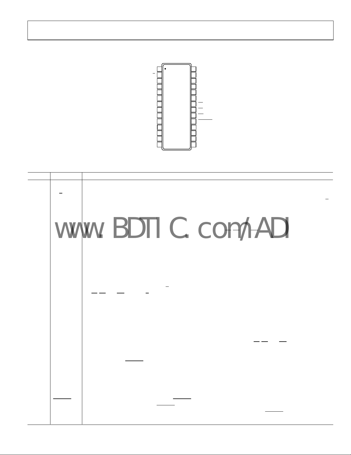
PIN CONFIGURATION AND FUNCTION DESCRIPTIONS
Table 6. Pin Function Descriptions
Pin No. Mnemonic Description
1 VDD
Power Supply Input. The V
with a 0.1 μF capacitor and a 10 μF tantalum capacitor.
2
W/B
Word/Byte Input. When this input is logic high, word transfer mode is enabled, and data is transferred to and from
the AD7933/AD7934 in 10-bit words on Pin DB2 to Pin DB11, or in 12-bit words on Pin DB0 to Pin DB11. When W/B
is logic low, byte transfer mode is enabled. Data and the channel ID are transferred on Pin DB0 to Pin DB7, and Pin
DB8/HBEN assumes its HBEN functionality. When operating in byte transfer mode, tie off unused data lines to
DGND.
3 to 10 DB0 to DB7
Data Bit 0 to Data Bit 7. Three-state parallel digital I/O pin
programming of the control register. These pins are controlled by CS
levels for these pins are determined by the V
DB1) are always 0, and the LSB of the conversion result is available on DB2.
11 V
DRIVE
Logic Power Supply Input. The voltage supplied at this pin determines at what voltage the parallel interface of the
AD7933/AD793
should never exceed V
12 DGND
Digital Ground. This is the ground reference point for all dig
to the DGND plane of a system. The DGND and AGND voltages should ideally be at the same potential and must
not be more than 0.3 V apart, even on a transient basis.
13 DB8/HBEN
Data Bit 8/High Byte Enable. When W/B
, RD, and WR. When W/B is low, this pin acts as the high byte enable pin. When HBEN is low, the low byte of
by CS
data written to or read from the AD7933/AD7934 is on DB0 to DB7. When HBEN is high, the top four bits of the
data being written to, or read from, the AD7933/AD7934 are on DB0 to DB3. When reading from the device, DB4
and DB5 contain the ID of the channel to which the conversion result corresponds (see the channel address bits in
Table 10). DB6 and DB7 are always 0. When writing to the device
Note that when reading from the AD7933, the two LSBs in the low byte are 0s, and the remaining six bits are
conversion data.
14 to
16
DB9 to
DB11
Data Bit 9 to Data Bit 11. Three-state parallel digital I/O pins that provide the conversion result and also allow the
control register to be programmed in word mode. These pins are controlled by CS, RD, and WR. The logic high/low
voltage levels for these pins are determined by the V
17 BUSY
Busy Output. This is the logic output indicating the status of the conversion.
the falling edge of CONVST
the result is available in the output register, the BUSY output goes low. The track-and-hold returns to track mode
just prior to the falling edge of BUSY, on the 13
18 CLKIN
Master Clock Input. The clock source for the conversion proc
AD7933/AD7934 takes 13 clock cycles + t
conversion time and achievable throughput rate. The CLKIN signal can be a continuous or burst clock.
19
CONVST
Conversion Start Input. A falling edge on CONVST initiates a conversion. The track-and-hold goes from track to
hold mode on the falling edge of CONVST
down, when operating in the autoshutdown or autostandby mode, a rising edge on CONVST is used to power up
the device.
1
V
DD
2
W/B
3
DB0
4
DB1
DB2
DB3
DB4
DB5
DB6
DB7
V
DRIVE
DGND
DB8/HBEN DB11
DB9
5
6
(Not to Scale)
7
8
9
10
11
12
13
14
AD7933/
AD7934
TOP VIEW
28
V
IN
27
VIN2
26
V
IN
25
V
IN
24
V
REFIN/VREFOU
23
AGND
22
CS
21
RD
20
WR
19
CONVST
18
CLKIN
17
BUSY
16
15
DB10
3
1
0
03713-006
Figure 2. Pin Configuration
range for the AD7933/AD7934 is from 2.7 V to 5.25 V. Decouple the supply to AGND
DD
s that provide the conversion result and allow
, RD, and WR. The logic high/low voltage
input. When reading from the AD7933, the two LSBs (DB0 and
DRIVE
4 operates. Decouple this pin to DGND. The voltage at this pin may be different to that at V
by more than 0.3 V.
DD
ital circuitry on the AD7933/AD7934. Connect this pin
is high, this pin acts as Data Bit 8, a three-state I/O pin that is controlled
, DB4 to DB7 of the high byte must be all 0s.
input.
DRIVE
The BUSY output goes high following
and stays high for the duration of the conversion. Once the conversion is complete and
th
rising edge of CLKIN (see Figure 34).
ess is applied to this pin. Conversion time for the
. The frequency of the master clock input therefore determines the
2
, and the conversion process is initiated at this point. Following power-
DD
but
Rev. B | Page 9 of 32
AD7933/AD7934
www.BDTIC.com/ADI
Pin No. Mnemonic Description
20
21
22
23 AGND
24 V
25 to
28
Write Input. Active low logic input used in conjunction with CS to write data to the control register.
WR
Read Input. Active low logic input used in conjunction with CS to access the conversion result. The conversion
RD
result is placed on the data bus following the falling edge of RD read while CS is low.
Chip Select. Active low logic input used in conjunction with RD and WR to read conversion data or write data to
CS
the control register.
cuitry on the AD7933/AD7934. All analog input
t are multiplexed into the on-chip track-and-
REFIN/VREFOUT
V
0 to VIN3
IN
Analog Ground. This is the ground reference point for all analog cir
signals and any external reference signal should be referred to this AGND voltage. The AGND and DGND voltages
should ideally be at the same potential and must not be more than 0.3 V apart, even on a transient basis.
Reference Input/Output. This pin is connected to the internal reference and is the reference source for the ADC.
The nominal i
V
REFIN/VREFOUT
voltage range for the external reference is 0.1 V to V
exceed V
Analog Input 0 to Analog Input 3. Four analog input channels tha
hold. The analog inputs can be programmed as four single-ended inputs, two fully differential pairs, or two pseudo
differential pairs by appropriately setting the MODE bits in the control register (see Table 10). Select the analog
input channe
prior to the conversion, or by using the on-chip sequencer. The input range for all input channels can either be 0 V
to V
REF
and CODING bits in the control register. To avoid noise pickup, connect any unused input channels to AGND.
nternal reference voltage is 2.5 V, and this appears at this pin. It is recommended to decouple the
pin to AGND with a 470 nF capacitor. This pin can be overdriven by an external reference. The input
; however, ensure that the analog input range does not
+ 0.3 V. See the Reference section.
DD
l to be converted either by writing to Address Bit ADD1 and Address Bit ADD0 in the control register
or 0 V to 2 × V
, and the coding can be binary or twos complement, depending on the states of the RANGE
REF
DD
Rev. B | Page 10 of 32
 Loading...