Analog Devices AD7927 Datasheet
8-Channel, 200 kSPS, 12-Bit ADC
with Sequencer in 20-Lead TSSOP
AD7927
FEATURES
Fast Throughput Rate: 200 kSPS
Specified for AV
of 2.7 V to 5.25 V
DD
Low Power:
3.6 mW Max at 200 kSPS with 3 V Supply
7.5 mW Max at 200 kSPS with 5 V Supply
8 (Single-Ended) Inputs with Sequencer
Wide Input Bandwidth:
70 dB Min SINAD at 50 kHz Input Frequency
Flexible Power/Serial Clock Speed Management
No Pipeline Delays
High Speed Serial Interface SPI™/QSPI™/
MICROWIRE™/DSP Compatible
Shutdown Mode: 0.5
A Max
20-Lead TSSOP Package
GENERAL DESCRIPTION
The AD7927 is a 12-bit, high speed, low power, 8-channel,
successive-approximation ADC. The part operates from a single
2.7 V to 5.25 V power supply and features throughput rates up
to 200 kSPS. The part contains a low noise, wide bandwidth
track-and-hold amplifier that can handle input frequencies in
excess of 8 MHz.
The conversion process and data acquisition are controlled
using CS and the serial clock signal, allowing the device to
easily interface with microprocessors or DSPs. The input signal
is sampled on the falling edge of CS and the conversion is also
initiated at this point. There are no pipeline delays associated
with the part.
The AD7927 uses advanced design techniques to achieve very low
power dissipation at maximum throughput rates. At maximum
throughput rates, the AD7927 consumes 1.2 mA maximum
with 3 V supplies; with 5 V supplies, the current consumption is
1.5 mA maximum.
Through the configuration of the Control Register, the analog
input range for the part can be selected as 0 V to REF
2 ¥ REF
, with either straight binary or twos complement output
IN
or 0 V to
IN
coding. The AD7927 features eight single-ended analog inputs
with a channel sequencer to allow a preprogrammed selection of
channels to be converted sequentially.
The conversion time for the AD7927 is determined by the SCLK
frequency, as this is also used as the master clock to control the
conversion. The conversion time may be as short as 800 ns with
a 20 MHz SCLK.
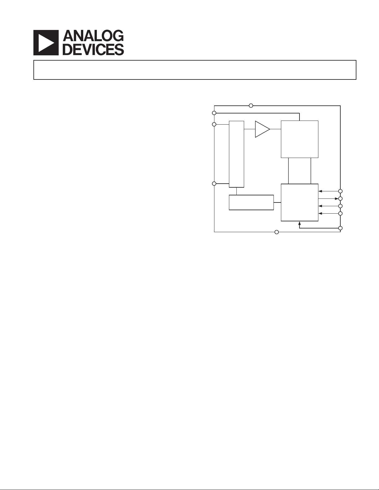
FUNCTIONAL BLOCK DIAGRAM
AV
DD
REF
IN
VIN0
V
IN
•
•
•
•
•
•
•
•
•
•
•
•
•
7
I/P
MUX
AD7927
T/H
SEQUENCER
APPROXIMATION
CONTROL LOGIC
GND
12-BIT
SUCCESSIVE
ADC
SCLK
DOUT
DIN
CS
V
DRIVE
PRODUCT HIGHLIGHTS
1. High Throughput with Low Power Consumption.
The AD7927 offers up to 200 kSPS throughput rates. At the
maximum throughput rate with 3 V supplies, the AD7927
dissipates 3.6 mW of power maximum.
2. Eight Single-Ended Inputs with a Channel Sequencer.
A consecutive sequence of channels, through which the ADC
will cycle and convert on, can be selected.
3. Single-Supply Operation with V
DRIVE
Function.
The AD7927 operates from a single 2.7 V to 5.25 V supply. The
function allows the serial interface to connect directly
V
DRIVE
to either 3 V or 5 V processor systems independent of AV
DD
4. Flexible Power/Serial Clock Speed Management.
The conversion rate is determined by the serial clock, allowing
the conversion time to be reduced through the serial clock
speed increase. The part also features various shutdown modes
to maximize power efficiency at lower throughput rates. Current
consumption is 0.5 mA maximum when in full shutdown.
5. No Pipeline Delay.
The part features a standard successive-approximation ADC
with accurate control of the sampling instant via a CS input
and once off conversion control.
.
REV. 0
Information furnished by Analog Devices is believed to be accurate and
reliable. However, no responsibility is assumed by Analog Devices for its
use, nor for any infringements of patents or other rights of third parties that
may result from its use. No license is granted by implication or otherwise
under any patent or patent rights of Analog Devices. Trademarks and
registered trademarks are the property of their respective companies.
One Technology Way, P.O. Box 9106, Norwood, MA 02062-9106, U.S.A.
Tel: 781/329-4700 www.analog.com
Fax: 781/326-8703 © 2003 Analog Devices, Inc. All rights reserved.

AD7927–SPECIFICATIONS
(AVDD = V
= 2.7 V to 5.25 V, REFIN = 2.5 V, f
DRIVE
otherwise noted.)
= 20 MHz, TA = T
SCLK
MIN
to T
, unless
MAX
Parameter B Version
DYNAMIC PERFORMANCE f
Signal-to-(Noise + Distortion) (SINAD)
Signal-to-Noise Ratio (SNR)
2
Total Harmonic Distortion (THD)
2
70 dB min @ 5 V
69 dB min @ 3 V Typically 70 dB
2
70 dB min
–77 dB max @ 5 V Typically –84 dB
1
Unit Test Conditions/Comments
= 50 kHz Sine Wave, f
IN
SCLK
= 20 MHz
–73 dB max @ 3 V Typically –77 dB
Peak Harmonic or Spurious Noise –78 dB max @ 5 V Typically –86 dB
(SFDR)
Intermodulation Distortion (IMD)
2
2
–76 dB max @ 3 V Typically –80 dB
fa = 40.1 kHz, fb = 41.5 kHz
Second Order Terms –90 dB typ
Third Order Terms –90 dB typ
Aperture Delay 10 ns typ
Aperture Jitter 50 ps typ
Channel-to-Channel Isolation
2
–82 dB typ fIN = 400 kHz
Full Power Bandwidth 8.2 MHz typ @ 3 dB
1.6 MHz typ @ 0.1 dB
DC ACCURACY
2
Resolution 12 Bits
Integral Nonlinearity ± 1 LSB max
Differential Nonlinearity –0.9/+1.5 LSB max Guaranteed No Missed Codes to 12 Bits
0 V to REF
Input Range Straight Binary Output Coding
IN
Offset Error ± 8 LSB max Typically ± 0.5 LSB
Offset Error Match ± 0.5 LSB max
Gain Error ± 1.5 LSB max
Gain Error Match ± 0.5 LSB max
0 V to 2 ¥ REF
Input Range –REFIN to +REFIN Biased about REFIN with
IN
Positive Gain Error ± 1.5 LSB max Twos Complement Output Coding
Positive Gain Error Match ± 0.5 LSB max
Zero Code Error ± 8 LSB max Typically ± 0.8 LSB
Zero Code Error Match ± 0.5 LSB max
Negative Gain Error ± 1 LSB max
Negative Gain Error Match ± 0.5 LSB max
ANALOG INPUT
Input Voltage Ranges 0 to REF
0 to 2 ¥ REF
V RANGE Bit Set to 1
IN
V RANGE Bit Set to 0, AVDD/V
IN
= 4.75 V to 5.25 V
DRIVE
DC Leakage Current ± 1 mA max
Input Capacitance 20 pF typ f
SAMPLE
= 200 kSPS
REFERENCE INPUT
REFIN Input Voltage 2.5 V ± 1% Specified Performance
DC Leakage Current ± 1 mA max
REFIN Input Impedance 36 kW typ
LOGIC INPUTS
Input High Voltage, V
Input Low Voltage, V
Input Current, I
Input Capacitance, C
INL
IN
IN
INH
3
0.7 ¥ V
DRIVE
0.3 ¥ V
DRIVE
± 1 mA max Typically 10 nA, V
10 pF max
V min
V max
= 0 V or V
IN
DRIVE
LOGIC OUTPUTS
Output High Voltage, V
Output Low Voltage, V
Floating-State Leakage Current ± 1 mA max
Floating-State Output Capacitance
OH
OL
3
V
– 0.2 V min I
DRIVE
0.4 V max I
10 pF max
= 200 mA, AVDD = 2.7 V to 5.25 V
SOURCE
= 200 mA
SINK
Output Coding Straight (Natural) Binary Coding Bit Set to 1
Twos Complement Coding Bit Set to 0
REV. 0–2–

Parameter B Version1Unit Test Conditions/Comments
CONVERSION RATE
Conversion Time 800 ns max 16 SCLK Cycles with SCLK at 20 MHz
Track-and-Hold Acquisition Time 300 ns max Sine Wave Input
300 ns max Full-Scale Step Input
Throughput Rate 200 kSPS max See Serial Interface Section
POWER REQUIREMENTS
AV
DD
V
DRIVE
4
I
DD
During Conversion 2.7 mA max AVDD = 4.75 V to 5.25 V, f
Normal Mode (Static) 600 mA typ AV
Normal Mode (Operational) f
Using Auto Shutdown Mode f
= 200 kSPS 1.5 mA max AVDD = 4.75 V to 5.25 V, f
SAMPLE
= 200 kSPS 900 mA typ AVDD = 4.75 V to 5.25 V, f
SAMPLE
2.7/5.25 V min/max
2.7/5.25 V min/max
Digital I/Ps = 0 V or V
2 mA max AV
1.2 mA max AV
650 mA typ AV
DRIVE
= 2.7 V to 3.6 V, f
DD
= 2.7 V to 5.25 V, SCLK On or Off
DD
= 2.7 V to 3.6 V, f
DD
= 2.7 V to 3.6 V, f
DD
SCLK
= 20 MHz
SCLK
= 20 MHz
SCLK
= 20 MHz
SCLK
= 20 MHz
SCLK
= 20 MHz
SCLK
= 20 MHz
Auto Shutdown (Static) 0.5 mA max SCLK On or Off (20 nA typ)
Full Shutdown Mode 0.5 mA max SCLK On or Off (20 nA typ)
Power Dissipation
Normal Mode (Operational) 7.5 mW max AVDD = 5 V, f
Auto Shutdown (Static) 2.5 mW max AV
Full Shutdown Mode 2.5 mW max AV
4
= 20 MHz
3.6 mW max AV
1.5 mW max AV
= 3 V, f
DD
= 5 V
DD
= 3 V
DD
= 5 V
DD
SCLK
= 20 MHz
SCLK
1.5 mW max AVDD = 3 V
NOTES
1
Temperature ranges as follows: B Version: –40∞ C to +85∞C.
2
See Terminology section.
3
Sample tested @ 25∞C to ensure compliance.
4
See Power versus Throughput Rate section.
Specifications subject to change without notice.
AD7927
REV. 0
–3–
AD7927
TIMING SPECIFICATIONS
Limit at T
1
(AVDD = 2.7 V to 5.25 V, V
, T
MAX
AD7927
MIN
ⱕ AVDD, REFIN = 2.5 V, TA = T
DRIVE
MIN
to T
, unless otherwise noted.)
MAX
Parameter AVDD = 3 V AVDD = 5 V Unit Description
2
f
SCLK
10 10 kHz min
20 20 MHz max
t
CONVERT
t
QUIET
16 ¥ t
SCLK
50 50 ns minMinimum Quiet Time Required between CS Rising Edge
16 ¥ t
SCLK
and Start of Next Conversion
t
2
3
t
3
3
t
4
t
5
t
6
t
7
4
t
8
t
9
t
10
t
11
t
12
10 10 ns min CS to SCLK Setup Time
35 30 ns max Delay from CS until DOUT Three-State Disabled
40 40 ns max Data Access Time after SCLK Falling Edge
0.4 ¥ t
0.4 ¥ t
SCLK
SCLK
0.4 ¥ t
0.4 ¥ t
SCLK
SCLK
ns min SCLK Low Pulsewidth
ns min SCLK High Pulsewidth
10 10 ns min SCLK to DOUT Valid Hold Time
15/45 15/35 ns min/max SCLK Falling Edge to DOUT High Impedance
10 10 ns min DIN Setup Time Prior to SCLK Falling Edge
55 ns min DIN Hold Time after SCLK Falling Edge
20 20 ns min Sixteenth SCLK Falling Edge to CS High
11 ms max Power-Up Time from Full Power-Down/Auto
Shutdown Mode
NOTES
1
Sample tested at 25∞C to ensure compliance. All input signals are specified with tr = tf = 5 ns (10% to 90% of AVDD) and timed from a voltage level of 1.6 V.
See Figure 1. The 3 V operating range spans from 2.7 V to 3.6 V. The 5 V operating range spans from 4.75 V to 5.25 V.
2
Mark/Space ratio for the SCLK input is 40/60 to 60/40.
3
Measured with the load circuit of Figure 1 and defined as the time required for the output to cross 0.4 V or 0.7 ¥ V
4
t8 is derived from the measured time taken by the data outputs to change 0.5 V when loaded with the circuit of Figure 1. The measured number is then extrapolated
back to remove the effects of charging or discharging the 50 pF capacitor. This means the time, quoted in the timing characteristics t8, is the true bus relinquish time
of the part and is independent of the bus loading.
Specifications subject to change without notice.
DRIVE
.
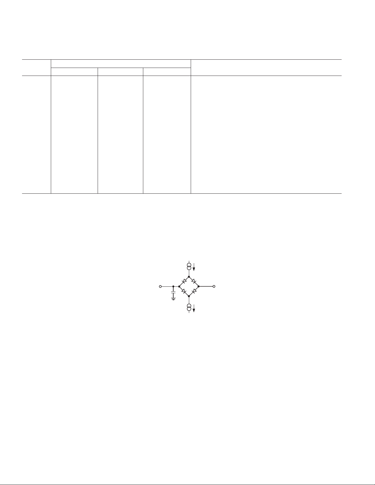
I
OL
1.6V
I
OH
OUTPUT
PIN
200A
TO
C
L
50pF
200A
Figure 1. Load Circuit for Digital Output Timing Specifications
REV. 0–4–

AD7927
ABSOLUTE MAXIMUM RATINGS
(TA = 25∞C, unless otherwise noted.)
1
AVDD to AGND . . . . . . . . . . . . . . . . . . . . . . . –0.3 V to +7 V
to AGND . . . . . . . . . . . . . . . . –0.3 V to AVDD + 0.3 V
V
DRIVE
Analog Input Voltage to AGND . . . . –0.3 V to AV
+ 0.3 V
DD
Digital Input Voltage to AGND . . . . . . . . . . . . –0.3 V to +7 V
Digital Output Voltage to AGND . . . . . –0.3 V to AV
to AGND . . . . . . . . . . . . . . . . –0.3 V to AVDD + 0.3 V
REF
IN
+ 0.3 V
DD
Input Current to Any Pin Except Supplies2 . . . . . . . . ± 10 mA
Operating Temperature Range
Commercial (B Version) . . . . . . . . . . . . . . –40∞C to +85∞C
Storage Temperature Range . . . . . . . . . . . –65∞C to +150∞C
Junction Temperature . . . . . . . . . . . . . . . . . . . . . . . . . . 150∞C
ORDERING GUIDE
Temperature Linearity Package Package
Model Range Error (LSB)
AD7927BRU –40∞C to +85∞C ± 1 RU-20 TSSOP
EVAL-AD7927CB
EVAL-CONTROL BRD2
NOTES
1
Linearity error here refers to integral linearity error.
2
This can be used as a standalone evaluation board or in conjunction with the Evaluation Controller Board for evaluation/demonstration purposes.
3
This board is a complete unit allowing a PC to control and communicate with all Analog Devices evaluation boards ending in the CB designators.
To order a complete evaluation kit, you will need to order the particular ADC evaluation board, e.g., EVAL-AD7927CB, the EVAL-CONTROL
BRD2, and a 12 V ac transformer. See the relevant Evaluation Board Application Note for more information.
2
3
TSSOP Package, Power Dissipation . . . . . . . . . . . . . 450 mW
Thermal Impedance . . . . . . . . . . . . . . 143∞C/W (TSSOP)
q
JA
Thermal Impedance . . . . . . . . . . . . . . . 45∞C/W (TSSOP)
q
JC
Lead Temperature, Soldering
Vapor Phase (60 sec) . . . . . . . . . . . . . . . . . . . . . . . . . 215∞C
Infrared (15 sec) . . . . . . . . . . . . . . . . . . . . . . . . . . . . 220∞C
ESD . . . . . . . . . . . . . . . . . . . . . . . . . . . . . . . . . . . . . . . . . 2 kV
NOTES
1
Stresses above those listed under Absolute Maximum Ratings may cause permanent damage to the device. This is a stress rating only and functional operation of
the device at these or any other conditions above those listed in the operational
sections of this specification is not implied. Exposure to absolute maximum rating
conditions for extended periods may affect device reliability.
2
Transient currents of up to 100 mA will not cause SCR latch-up.
1
Option Description
Evaluation Board
Controller Board
CAUTION
ESD (electrostatic discharge) sensitive device. Electrostatic charges as high as 4000 V readily
accumulate on the human body and test equipment and can discharge without detection. Although the
AD7927 features proprietary ESD protection circuitry, permanent damage may occur on devices
subjected to high energy electrostatic discharges. Therefore, proper ESD precautions are recommended
to avoid performance degradation or loss of functionality.
REV. 0
–5–
AD7927
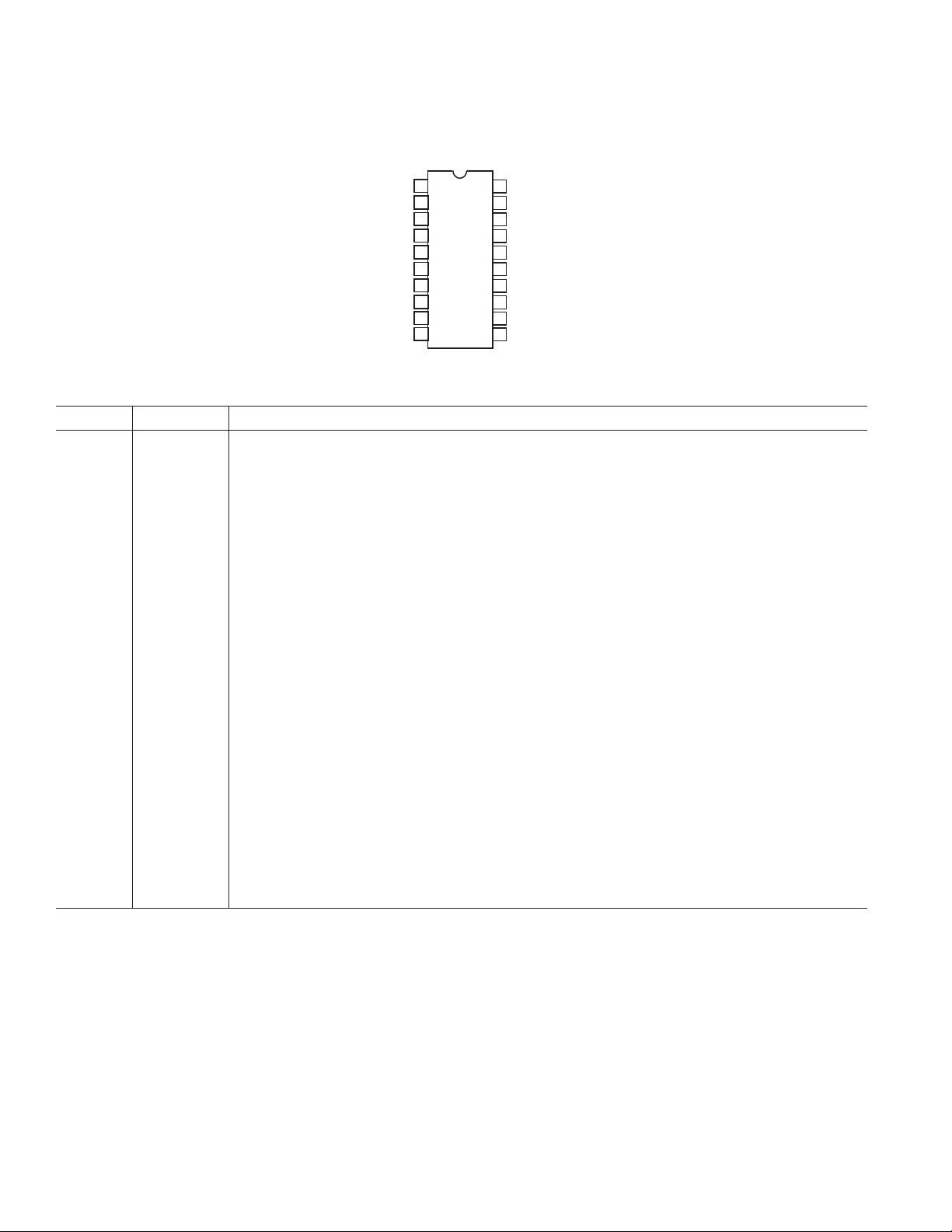
PIN CONFIGURATION
20-Lead TSSOP
1
SCLK AGND
2
DIN V
3
CS
AD7927
4
AGND AGND
AV
AV
REF
AGND VIN3
TOP VIEW
(Not to Scale)
5
DD
6
DD
7
IN
8
9
VIN7V
10
VIN6V
20
19
18
17
16
15
14
13
12
11
DRIVE
DOUT
VIN0
VIN1
VIN2
IN
IN
4
5
PIN FUNCTION DESCRIPTIONS
Pin No. Mnemonic Function
1 SCLK Serial Clock. Logic input. SCLK provides the serial clock for accessing data from the part. This clock
input is also used as the clock source for the AD7927s conversion process.
2DIN Data In. Logic input. Data to be written to the AD7927s Control Register is provided on this input
and is clocked into the register on the falling edge of SCLK (see the Control Register section).
3 CS Chip Select. Active low logic input. This input provides the dual function of initiating conversions on
the AD7927 and framing the serial data transfer.
4, 8, 17, 20 AGND Analog Ground. Ground reference point for all analog circuitry on the AD7927. All analog input
signals and any external reference signal should be referred to this AGND voltage. All AGND pins
should be connected together.
5, 6 AV
7 REF
DD
IN
Analog Power Supply Input. The AVDD range for the AD7927 is from 2.7 V to 5.25 V. For the
0V to 2 ¥ REF
range, AVDD should be from 4.75 V to 5.25 V.
IN
Reference Input for the AD7927. An external reference must be applied to this input. The voltage
range for the external reference is 2.5 V ± 1% for specified performance.
16–9V
0–VIN7Analog Input 0 through Analog Input 7. Eight single-ended analog input channels that are multiplexed
IN
into the on-chip track-and-hold. The analog input channel to be converted is selected by using the
address bits ADD2 through ADD0 of the Control Register. The address bits in conjunction with the
SEQ and SHADOW bits allow the sequencer to be programmed. The input range for all input channels
can extend from 0 V to REF
or 0 V to 2 ¥ REFIN, as selected via the RANGE bit in the Control Register.
IN
Any unused input channels should be connected to AGND to avoid noise pickup.
18 DOUT Data Out. Logic output. The conversion result from the AD7927 is provided on this output as a serial
data stream. The bits are clocked out on the falling edge of the SCLK input. The data stream from the
AD7927 consists of two leading zeros, two address bits indicating which channel the conversion result
corresponds to, followed by the 12 bits of conversion data, MSB first. The output coding may be
selected as straight binary or twos complement via the CODING bit in the Control Register.
19 V
DRIVE
Logic Power Supply Input. The voltage supplied at this pin determines at what voltage the serial interface
of the AD7927 will operate.
REV. 0–6–
 Loading...